Ideally, the resonance should be critically damped (Q=0.5), which can be achieved by adding external series resistance to the choke. Strictly, the load resistance across the capacitor also damps the resonance, and this may be transformed into a notional extra choke series resistance using:
However, the damping effect of the load resistance is usually negligible. Even worse, a series voltage regulator is a constant current, or infinite, AC load to the smoothing circuitry, so it adds no damping whatsoever.
A typical traditional example: A choke input supply might use a 15 H choke having 260 Ω internal resistance coupled to an 8 μF capacitor, resulting in fres(Low Frequency)=15 Hz and Q=5.3. This Q is too high, and fres(Low Frequency) is too near the audio band, but the additional 2.5 kΩ series resistance required to achieve critical damping would waste HT voltage and greatly increase power supply output resistance. A better alternative would replace the 8 μF capacitor with a 120 μF polypropylene, since this would give fres(Low Frequency)=3.75 Hz and Q=1.36, and this Q might be acceptable. Note that reducing Q by increasing C is not as effective as increasing R because C is inside the square root term of the Q equation, so when simulating in PSUD2, expect the need to increase filter capacitance significantly if you can’t tolerate increased choke resistance.
Region 2
The reactance of the choke doubles for each octave rise in frequency, whilst the reactance of the reservoir capacitor halves, producing the familiar 12 dB/octave slope. PSUD2 works in the time rather than frequency domain, so we don’t see this directly, but the reported values of ripple tell us how well we are filtering at our chosen ripple frequency.
Note that PSUD2 has no understanding of the next two concepts, so both concepts must be checked manually.
Region 3
The choke’s internal shunt capacitance begins to take effect. Once the reactance of the shunt capacitance is equal to the inductive reactance of the choke, the choke resonates, so this region may be defined as beginning at fres(high frequency). Above this self-resonant frequency (3–15 kHz for a typical HT choke), the choke’s shunt capacitance forms a potential divider with the filter capacitance whose loss is constant with frequency:
Region 4
The series inductance of the filter capacitor becomes significant, and this forms a hidden high-pass filter in conjunction with the shunt capacitance of the choke, so the output noise of the practical filter rises at 12 dB/octave.
All of the previous concepts can be simplified by considering an idealised LC filter response to be made up of three straight lines having freedom to move either vertically or horizontally (see Figure 5.30).
• Line A falls at 12 dB/octave, and slides horizontally to the left as the product of choke inductance and filter capacitance increases.
• Line B falls vertically as the ratio of filter capacitance and choke shunt capacitance increases, intercepting line A at the choke’s self-resonant frequency. Capacitance between adjacent winding layers of the choke could be reduced by vertical sectioning or by interposing earthed electrostatic screens.
• Line C rises at 12 dB/octave, and slides horizontally to the right as filter capacitor series inductance falls, intercepting line B at the capacitor’s self-resonant frequency. Most modern capacitors have series inductance between 10 nH and 100 nH, so if this value is known, their self-resonant frequency can be calculated using the standard resonance equation. Conversely, if their self-resonant frequency is known, series inductance can be calculated. Sadly, the two preceding statements are not true for an electrolytic capacitor – the capacitance of an electrolytic capacitor at self-resonance is likely to be between 25% and 50% lower than its DC value.
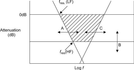
Unfortunately, filter capacitor ESR also complicates the issue and can easily mask the plateau of line B. The intersection of lines B and C can be viewed as the response of an LC filter, but plotted upside down. Thus, to avoid degrading the plateau, the Q of the capacitor’s self-resonant frequency should be >1/√2 (unusually, we want the filter’s response to be underdamped at its resonant frequency). Remembering:
Rearranging and inserting our Q requirement:
Thus, a 100 μF filter capacitor having a typical series inductance of 20 nH would require ESR<18 mΩ.
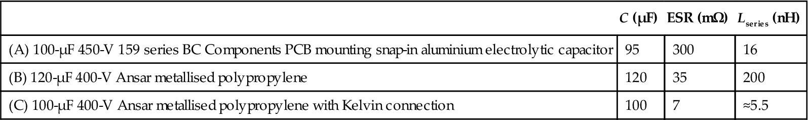
The modelled filter compares the effect of the measured parameters of three different filter capacitors in combination with a Woden 51700 choke (20 H, 365 Ω and 95 pF) (see Figure 5.31 and Table 5.5).
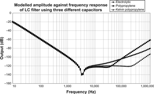
Table 5.5
Capacitor Values and Parasitic Components of the Modelled Filter of Figure 5.31
| C (μF) | ESR (mΩ) | Lseries (nH) | |
| (A) 100-μF 450-V 159 series BC Components PCB mounting snap-in aluminium electrolytic capacitor | 95 | 300 | 16 |
| (B) 120-μF 400-V Ansar metallised polypropylene | 120 | 35 | 200 |
| (C) 100-μF 400-V Ansar metallised polypropylene with Kelvin connection | 100 | 7 | ≈5.5 |
As expected, the electrolytic capacitor fails to achieve the filtering plateau due to its significant ESR. Capacitor B had the potential to offer excellent broadband filtering, but its ESR and series inductance were badly compromised by an ill-considered mechanical requirement to have both leads (known as tails) exit from the same end, enforcing an additional 120 mm length on one tail.
Capacitor C with its Kelvin connection was from the second batch specially made for the author by suppression devices of clitheroe but will doubtless become a standard part. Note that not only does capacitor C easily achieve the filtering plateau, but also that its minimal series inductance maintains that plateau to the highest frequency. Each end of the capacitor has two independent tails from the tin/zinc layer connecting to the plates: one tail is used for the source of current and the other for the load (see Figure 5.32).
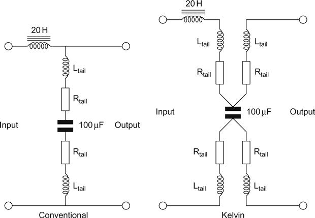
The significance of the Kelvin connection is that from the point of view of filtering incoming interference, tail inductance (typically 0.75 nH/mm) and resistance are no longer relevant, and filtering is determined purely by the residual inductance and resistance of the foils. This connection is also useful when the capacitor is used as a reservoir capacitor because it enables ideal separation of ripple current from load current. Most importantly, if a plastic capacitor has to be used (usually because of the required voltage rating) Kelvin connection offers a significant reduction of mains-borne interference between 10 kHz and 1 MHz at insignificant additional cost.
The modelled Kelvin connection shows a significant improvement, but does it match reality? (see Figure 5.33).
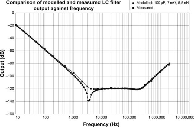
As can be seen, the match isn’t quite perfect, with meter noise causing a shallower null at the choke’s self-resonant frequency than modelled, but the general correspondence is excellent, and matching the model to the measurement was the only practical way of determining the Kelvin capacitor’s series inductance and ESR. More importantly, the hypothesised improved high-frequency filtering of the Kelvin connection was confirmed.
Summarising, the ideal practical LC filter achieves the plateau of line B and maintains it to a high frequency. The limiting factors are choke self-resonant frequency, filter capacitor ESR and Lseries, so the ideal LC filter uses a capacitor having a Kelvin connection.
Estimation of Wide-Band LC Response
The significance of the LC model is that once we know the self-resonant frequency of the iron choke, we also know where the filter’s attenuation becomes constant. Further, since we know that the line down to the self-resonant frequency falls at 12 dB/octave (or 40 dB/decade, if you prefer), we know the maximum high-frequency attenuation. It is easy to measure a choke’s self-resonant frequency using an oscillator and an oscilloscope, but that takes time, and we might need a quick ‘down and dirty’ estimation. The author measured the self-resonant frequency of a number of HT chokes and plotted this against their inductance (see Figure 5.34).
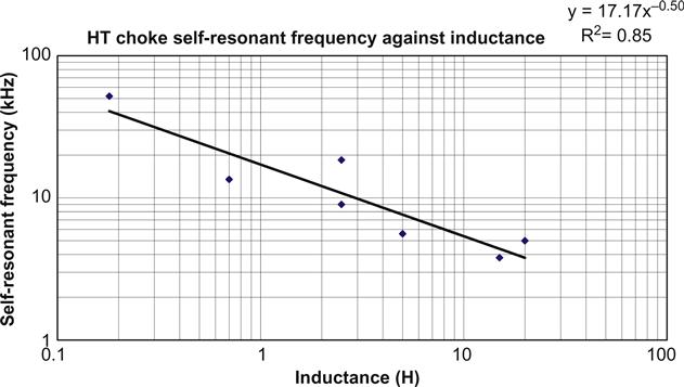
The graph shows that we can estimate a choke’s self-resonant frequency as being 20 divided by the square root of its inductance. As an example, if we were wondering about the suitability of a 16 H choke, we could estimate its self-resonant frequency as being 5 kHz. Further, we could note that from 100 Hz to 5 kHz is roughly five-and-a-half octaves, so we would know that the maximum attenuation compared to 100 Hz would be 5.5×12≈66 dB. If we had already simulated the choke and accompanying capacitor in PSUD2, we would know the expected ripple at 100 Hz, so we would now have an estimate of the noise at the line B plateau. Obviously, if we knew the exact values of all the parasitic components in our LC filter, we could model it in T/spice. However, it takes time and a little care to determine these values to any degree of accuracy, so if we are happy with a result accurate to ±6 dB, an estimation is fine.
Sectioned RC Filters
We might have carefully designed the first stage of an HT power supply (choke or capacitor input) with the available parts so that it produces 2 Vpk–pk of ripple, yet we might need ripple <1 mVpk–pk, but could afford to drop some DC voltage. Thus, we need a filter that can attenuate the ripple by a factor of >2,000. Since an RC filter is a potential divider, the attenuation is R/Xc (provided that this ratio is reasonably large). Suppose that in our example, we can tolerate 2 kΩ of resistance, so Xc=2 kΩ/2,000=1 Ω. Since the ripple frequency is 100 Hz, we find the required capacitance using:
This is a very large capacitor and represents a brute force solution to the problem. A more efficient alternative is to make a filter out of a cascade of sections each using a smaller resistor and capacitor (see Figure 5.35).
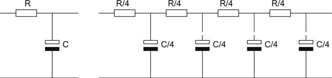
The problem is to determine how many sections are ideal. Fortunately, Scroggie [12] (writing as ‘Cathode Ray’) has already investigated this problem and produced Table 5.6.
Table 5.6
Cascaded Section Coefficients (after Scroggie)
| No. of sections | 2πfCR (Rtotal/Xc) | Attenuation | RC in kΩ·μF per section | |
| 100 Hz | 120 Hz | |||
| 1 | 16 | 16 | 25.5 | 21.2 |
| 2 | 45.6 | 130 | 18.1 | 15.1 |
| 3 | 90 | 997 | 15.9 | 13.3 |
| 4 | 149 | 7,520 | 14.8 | 12.4 |
| 5 | 223 | 56,400 | 14.2 | 11.8 |
| 6 | 311 | 420,000 | 13.8 | 11.5 |

Some values in Table 5.6 differ from the original reference because Scroggie did not have the benefit of a spreadsheet to accurately calculate his values.
To understand Table 5.6 using our previous example, we need attenuation >2,000, so the first number of sections that can exceed this in the attenuation column is n=4. If the resistance must total 2 kΩ, each section must be 2 kΩ/4=500 Ω. To find the individual capacitance required, we use the 100 Hz RC column. The capacitance required is 14.8/0.5=29.6 μF. In practice, we would probably use 470 Ω resistors and 33 μF capacitors. The key point is not just that the four 33 μF capacitors are likely to be much cheaper (and smaller) than a single ≈1,590 μF capacitor, but that the sectioned filter promises almost four times the attenuation. PSUD2 can analyse multiple RC filters, so the combination of Scroggie’s table and a PSUD2 simulation can be very effective.
Alternatively, you might have a large bag of 22 μF capacitors, and enough room to use four, but must use 2.5 kΩ of series resistance. How can the capacitors be best used to attenuate 100 Hz ripple? Connecting the four capacitors in parallel gives a total capacitance of 88 μF, so the ratio of Rtotal/Xc=138. Inspecting the Rtotal/Xc column, 90 is the first solution exceeded by 138, so three sections should be used. Each resistance is thus 2.5 kΩ/3=833 Ω. If we only use three sections, our total ratio R/Xc is reduced by a factor of 3/4, so it falls to 104, but this is still optimum with three sections and gives an attenuation of 997, whereas using four parallel 22 μF capacitors with a 2.5 kΩ series resistor would only have given an attenuation of 138. Our factor of improvement is 7, yet we have used one fewer capacitor (saving space).
Regulators
The best way of improving a power supply is to use a voltage regulator. A voltage regulator is a real-world approximation of a Thévenin source; it has a fixed output voltage and an output resistance that approaches zero. A true Thévenin source implies infinite current capacity, whereas the supply that feeds a regulator has limited current capacity. It is therefore important to realise that the regulator can only simulate a Thévenin source over a limited range of operation, so we must ensure that we remain within this range under all possible operating conditions.
All voltage regulators are based on the potential divider. Either the upper or the lower leg of the divider is made controllable in some way, and by this means, the output voltage can be varied (see Figure 5.36).
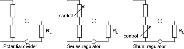
If the upper element is made controllable, then the regulator is known as a series regulator because the controlled element is in series with the load. If the lower leg of the divider is controlled, then the regulator is known as a shunt regulator because this element is shunted by the load. Shunt regulators are usually inefficient compared to series regulators, and their design has to be carefully tailored to their load, but they have the advantage that they can both source and sink current.
The Fundamental Series Regulator
The fundamental elements of a series voltage regulator are shown in Figure 5.37.
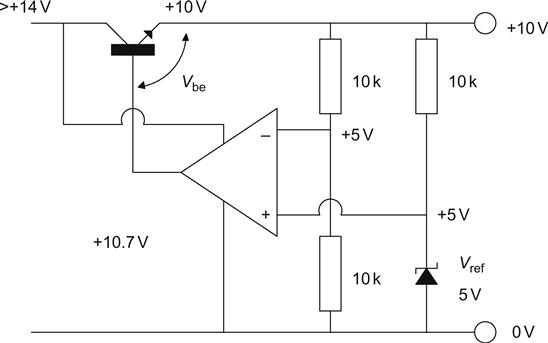
The circuit shown uses semiconductors, but a valve version could equally well be built. The error amplifier amplifies the difference between the reference voltage and a fraction of the output voltage and controls the series pass transistor such that a stable output voltage is achieved.
The circuit depends for its operation on negative feedback. We saw in Chapter 1 that when feedback is applied, input and output resistances change by ratio of the feedback factor (1+βA0). Voltage regulators rely on shunt-derived feedback reducing the output resistance of the system by the ratio of the feedback factor.
Suppose initially that the regulator is working and that there is 10 V at the output. By potential divider action, there must be 5 V on the inverting input of the operational amplifier. The voltage reference is holding the non-inverting input at 5 V. The series pass transistor is an emitter follower fed by the error amplifier, and has 10 V on its emitter, so the base must be at 10.7 V.
Suppose now that the output voltage falls for some reason. The voltage at the midpoint of the potential divider now falls, but the voltage reference maintains 5 V. The error amplifier now has a higher voltage on its non-inverting input than on its inverting input, and its output voltage must rise. If the voltage on the base of the transistor rises, its emitter voltage must also rise. The circuit therefore opposes the reduction in output voltage.
Since the same argument works in reverse for a rise in output voltage, it follows that the circuit is stable and that the output voltage is determined by the combination of the potential divider and the reference voltage. If we redraw the regulator, we can see that it is simply a non-inverting amplifier whose gain is set by the potential divider and that it amplifies the reference voltage (see Figure 5.38).
By inspection, the output voltage is therefore:
Since the error amplifier simply amplifies the reference voltage, any noise on the reference will also be amplified, and we should feed it from as clean a supply as possible. Although the argument seems like a snake chasing its own tail, if we feed the reference from the output of the supply (which is clean), then the reference will be clean, and the output of the supply will also be clean. It might be thought that supplying the current for the reference voltage from the output voltage would cause instability, but this is not a problem in practice.
It should be noted that all regulators need an input voltage higher than their output voltage. The minimum allowable difference between these voltages before the regulator fails to operate correctly is known as the drop-out voltage (because the regulator ‘drops out’ of regulation). With this particular design it is only a few volts, but drop-out voltage for a valve version could be 40 V or more.
The Two-Transistor Series Regulator
The two-transistor series regulator is a very common and useful circuit (see Figure 5.39).
This circuit is popular because of its extreme cheapness, but despite that, its performance is really quite good. Q2, the series pass transistor, is fed from the collector of Q1, a common emitter amplifier. The emitter of Q1 is held at a constant voltage by the voltage reference, whilst its base is fed a fraction of the output voltage by the potential divider. If the output voltage rises, Q1 turns on harder, drawing more current, its collector voltage (connected to the base of Q2) falls, causing the emitter voltage of Q2 (which is the output voltage) to fall, thus counteracting the initial error.
This circuit is ideal for use as a bias voltage regulator in a power amplifier because we often need to drop more volts than an IC regulator would tolerate.
As presented, the circuit can only supply 50 mA of output current because the base current for Q2 is stolen from the collector current of Q1. If we increased the collector current of Q1, Q2 could steal more, and output current could be increased, but a better solution would be to replace Q2 with a Darlington transistor, which would need less base current. Alternatively, Q2 could be a power MOSFET, but it would need a gate-stopper resistor of ≈100 Ω soldered directly to its gate pin.
The Zener diode passes 12 mA, which is quite sufficient to ensure that it operates correctly, and has a stable output voltage with minimum noise. A 6.2 V Zener has been chosen because it has lowest temperature coefficient and lowest slope resistance, but it still produces some noise, so it is bypassed by the 47 μF capacitor.
The Speed-Up Capacitor [13]
This capacitor is connected across the far resistor of the potential divider. Its purpose is to increase the amount of negative feedback available at AC, and thereby reduce hum and noise. Since any linear regulator can be considered to be composed of an op-amp enclosed by a feedback loop, a generic graph may be drawn (see Figure 5.40a).
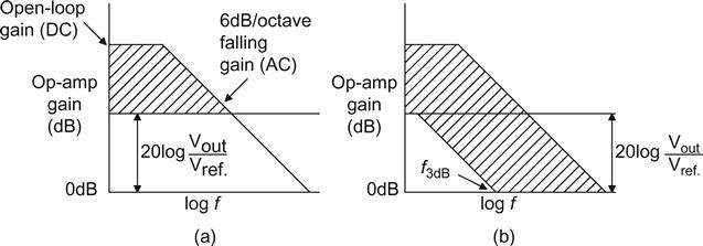
The op-amp gain is a combination of DC open-loop gain and gain that falls at 6 dB/octave with frequency. The gain within the hatched area is available for attenuating incoming ripple, so ripple reduction is maximised by:
• Maximising DC open-loop gain
• Maximising low frequency corner frequency (741: fcorner≈20 Hz; 5534: fcorner≈1 kHz)
• Minimising the ratio of DC output voltage to reference voltage.
Although we need the op-amp to have the correct gain at DC to set the output voltage correctly, the gain below the hatched area is wasted. The speed-up capacitor aims to recover some of this wasted gain (see Figure 5.40b).
At first sight, it would seem that f−3dB should be placed sufficiently low that all of the previously wasted gain is recovered. However, an oversized speed-up capacitor slugs the response of the regulator to changes in load current.
The maximum value for this capacitor is found by first calculating the AC Thévenin resistance that it sees:
Remembering that
and also that
we find that for this circuit, with hfe=200 and Ic=2 mA, hie≈2.9 kΩ. So the Thévenin resistance seen by the capacitor is ≈1.8 kΩ.
We would like the capacitor to have a significant effect on the lowest ripple frequency to be attenuated, which is 100 Hz (120 Hz US). The potential divider chain and capacitor is a step equaliser whose effect on the regulator is similar to that used for the RIAA 3,180 μs/318 μs pairing in Chapter 7. We could make the reactance of the capacitor at the lowest ripple frequency equal to the Thévenin resistance at the tapping of the potential divider, which would mean that an infinitely large capacitor could only improve ripple reduction by a further 3 dB:
The nearest value is 1 μF. This is quite a small capacitor, and the author has seen many similar circuits with oversized capacitors and, indeed, built one himself. The subjective effect of the oversize capacitor was to create a bass boom that was incorrectly thought at the time to be due to room acoustics when it was really due to the sluggish recovery of the power supply to transients.
At the opposite limit, we could set the reactance of the capacitor relative to the total resistance of the divider chain. The smaller capacitor would only give a 3 dB improvement in hum compared to a chain without a capacitor, but its low frequency transient response would be better than a regulator using a larger capacitor.
The value of the speed-up capacitor is a compromise between hum reduction and regulator low frequency transient response, so there isn’t a ‘correct’ answer here other than that the capacitor should be small. You might even want to determine its final value by listening because different loudspeakers (with different low frequency damping) can prefer different values.
Compensating for Regulator Output Inductance
The regulator also has a capacitor across its output. As shown in Figure 5.40, the gain of the error amplifier falls with frequency due to Miller effect and stray capacitances, so the amount of gain available for reducing output impedance falls. If (1+βA0) has fallen, then the output impedance must rise, and the effect is that output impedance rises with frequency. A perfect Thévenin source in series with an inductor would look identical, and for this reason the output of regulators is often described as being inductive at high frequencies. The output capacitor maintains a low output impedance at high frequencies.
A Variable Bias Voltage Regulator
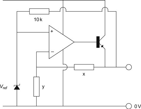
We often need a bias voltage regulator to be variable between certain limits. In this example, we will look at a grid bias regulator needed for an 845 directly heated triode. Perusal of RCA anode characteristics (circa 1933) indicated a grid bias voltage of −125 V, but modern valves do not match the original curves exactly, and we must equalise anode currents in this (push–pull) output stage to avoid saturating the output transformer with an unbalanced DC current and causing distortion. A range of ±25 V on either side of the nominal −125 V seems reasonable, but how do we design a regulator to fulfil this requirement?
Fortunately, since it supplies a part of the circuit where the signal voltages are very high (up to 90 VRMS), the regulator need not have an impeccable noise performance, and avalanche diodes are perfectly acceptable (see Figure 5.41).
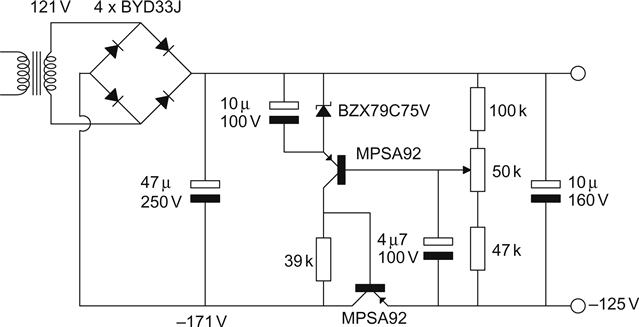
A higher-voltage reference allows the finished circuit to have better regulation, but we must still allow a reasonable voltage between the collector and the emitter of the control transistor. In practice, a reference voltage of about half the maximum output voltage is usually a good choice, and 75 V reference diodes are available.
The reference diode holds the emitter of the transistor at −75 V, and Vbe=0.7 V, so the base of the transistor will be held at a fixed potential of −75.7 V. Since the base of the transistor is connected to the wiper of the potential divider, the wiper must also be held at −75.7 V, no matter what output voltage is set. We can now calculate the required attenuation of the potential divider for the two extreme design cases:
By choosing a convenient value for the variable resistor in the middle of the potential divider, we now have enough information to calculate the required resistors on either side. A low value of variable resistor would require a large current to flow in the potential divider, whereas too high a value will cause errors due to the (small) base current drawn by the transistor. A good engineering principle is that the potential divider chain should pass roughly 10 times the expected base current, so a 50 kΩ variable resistor was a convenient standard value for this example.
When the wiper of the variable resistor is set to produce the largest voltage at the regulator output, it is connected directly to the grounded resistor (x), and vice versa. Using the standard potential divider equation, for −150 V:
And similarly for −100 V:
We now have two equations that can be solved, either simultaneously or by substitution, to give the values of the fixed resistors x and y. In this particular case, the values fell out very conveniently to give x=100 kΩ and y=47 kΩ, where x is the upper potential divider resistor and y is the lower potential divider resistor.
As a final note, bias supplies and their regulators draw very little current from their transformer, so a low current winding is used. Low current windings tend to have very poor regulation, and because their full-load current is rarely drawn, so the actual voltage at the theoretical −170 V point could easily be −180 V when measured.
The 317 IC Voltage Regulator
Although the two-transistor regulator is the ideal choice for a bias regulator because of its high voltage drop capability, once we need higher currents at lower voltages its limitations quickly become apparent.
It is perfectly possible to build a voltage regulator using a handful of components including an operational amplifier, a voltage reference, various transistors, resistors and capacitors. With care, the circuit can be made to work almost as well as an IC regulator and only costs about three times as much. We need not feel guilty about using IC regulators.
The 317 is a standard device that is made by all the major IC manufacturers [14]. Linear Technology [15] makes an upgraded version of the 317, the LT317, but the only difference is that the guaranteed tolerance of the voltage reference is tighter. A commercial design could therefore set its output voltage using fixed resistors rather than a variable resistor, thus saving money, because not only are variable resistors expensive to buy, they also have to be adjusted (which costs money). We do not often have to worry about such considerations, so the standard 317 is fine.
The 317 incorporates all of the fundamental elements of a series regulator in one three-terminal package, and we only need to add an external potential divider to produce an adjustable regulator (see Figure 5.42).

One end of the voltage reference is connected to the OUT terminal, whilst the other is an input to the error amplifier. The other input of the error amplifier is the ADJ terminal. The 317 therefore strives to maintain a voltage equal to its reference voltage (1.25 V) between the OUT and ADJ terminals. All we have to do is to set our potential divider so that the voltage at the tap is Vout=1.25 V, and the 317 will do the rest.
In datasheets for the 317, you will invariably find that the upper resistor of the potential divider is 240 Ω. The reason for this is that the 317 must pass 5 mA before it can regulate reliably. If the potential divider passes 5 mA, then this ensures that the device is able to regulate even if there is no external load.
The 317 sources ≈50 μA of bias current to the opposite rail from the ADJ pin, which therefore flows down the lower leg of the potential divider. Normally, this is negligible, but if you are designing a high voltage regulator, and choose a lower potential divider current, this will need to be taken into account.
The manufacturers’ data sheets generally show a regulator with the ADJ pin bypassed to ground by a 10 μF electrolytic, which improves ripple rejection from 60 dB to 80 dB at 100 Hz. This is the speed-up capacitor that we added to the two-transistor regulator, but because the reference voltage is tied to Vout, rather than ground, the speed-up capacitor connects to ground, rather than Vout.
We could therefore use the method derived earlier to check whether 10 μF is a reasonable value of capacitor. The ADJ pin is an input to an operational amplifier, so we can treat it as infinite input resistance, and we are only concerned with the external resistor values. If we were to use an upper resistor of 240 Ω, and a 2.7 kΩ lower resistor to set an output voltage of ≈15 V, then the maximum value would be 7.2 μF, so a 10 μF electrolytic capacitor is a reasonable choice, although the author would probably prefer 6.8 μF if he had one in stock.
Just like the two-transistor regulator, the output of the 317 is inductive, and the manufacturer’s output impedance curves suggest that the output impedance is equivalent to ≈2.2 μH in series with 2.7 mΩ when set to produce 10 V, so they recommend a 1 μF tantalum bead output bypass capacitor, as shown in the equivalent circuit (see Figure 5.43).
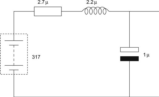
Assuming that the tantalum capacitor had zero ESR (!), the only damping resistance would be the 2.7 mΩ of the 317, so we have an underdamped resonant circuit, and we can calculate its Q:
Wiring resistance will reduce this Q considerably, but it will not reduce it to Q=0.5, which would be critically damped. This would not matter greatly because we would be unable to excite the circuit from the output (any external excitation would be short-circuited by the capacitor). If we now concede that the capacitor is not perfect, we may be unlucky enough to be able to excite the resonance, and the circuit could become unstable. Rearranging the formula, 3 Ω critically damps the resonance, and the IC manufacturers recommend 2.7 Ω in series with the tantalum capacitor.
The author measured a couple of 1.5 μF tantalum bead capacitors randomly picked from his parts bin and found one had an ESR of 4.8 Ω, whilst the other measured 2.7 Ω – negating any need for the series 2.7 Ω resistor. It does seem that tantalum bead capacitors have very variable ESR not just between manufacturers, but also between samples within batches, so data sheets either need to be read carefully or should be measured before use. An aluminium electrolytic capacitor plus series resistor would be a cheaper and less variable alternative.
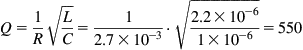
The 317 as an HT Regulator
Because the 317 is a floating regulator, there is no reason why it should not be used to regulate a 400 V HT supply. However, because the 317 can only tolerate 37 V from input to output, it needs support circuitry for protection [16] (see Figure 5.44).
The 317 is preceded by a high voltage transistor Darlington pair whose sole aim in life is to protect the 317 by maintaining 6.2 V−2 VBE−0.1ILOAD(mA) between its IN and OUT terminals. Unfortunately, the voltage drop across the 100 Ω resistor in this particular circuit means that the 317 drops out of regulation once load current >20 mA. The Darlington pair can easily cope with variations in mains voltage, but it should not be thought that this circuit is proof against a short-circuit when used at typical valve voltages.
Accidentally short-circuiting a regulator of this type with an oscilloscope probe results in an almighty bang, and all the silicon is destroyed. The author knows.
The lower arm of the potential divider is bypassed, but has a resistor in series with the capacitor to improve low frequency transient response by raising the lower f−3dB frequency of the step equaliser, and a diode has been added allegedly to discharge the capacitor in the event of an output short-circuit (although the author’s experience was that it didn’t actually help).
Variants of the Maida circuit are very popular as HT regulators, and the author has used many over the years (see the Crystal Palace amplifier in Chapter 6), but the circuit is fragile, and we will see later that it is possible to do better.
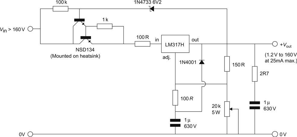
Valve Voltage Regulators
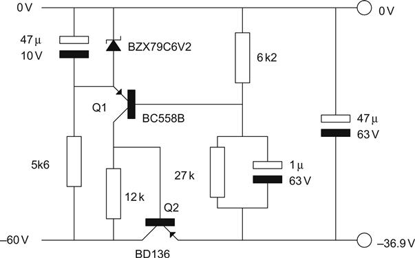
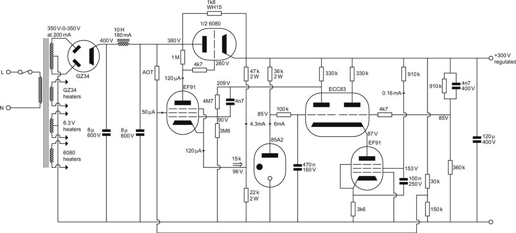
Valve voltage regulators have always been very rare, and we will now see why (see Figure 5.45).
The circuit is directly analogous to the two-transistor regulator; it simply has valves and higher voltages. The silicon reference diode has been replaced by a gas reference that holds the cathode of the EF86 stable at 85 V, whilst the grid is fed from the potential divider. The series pass element is a 6080 double triode (Pa(max)=13 W), which was specifically designed for use in series regulators and can pass high currents at low anode voltages.
A valve rectifier is used, and in deference to its limited ripple current capacity, an 8 μF paper/foil capacitor has been chosen for the reservoir, although a polypropylene capacitor (≤60 μF for this rectifier) would be physically practical. This results in considerable ripple voltage which is filtered by the following LC combination.
Unless the g2 resistor value is carefully chosen, the performance of the regulator is slightly compromised by feeding g2 of the EF86 from the raw supply, but if fed from the regulated supply, there is a danger that the circuit might simply sulk and not switch on. The gain of the EF86 is ≈100, and above ≈100 Hz this gain is available for reducing the output resistance of the 6080, whose gm≈7 mA/V, so rk≈200 Ω (including the effect of the external 100 Ω Ra). The regulator therefore achieves an output resistance of ≈2 Ω.
Each valve has its cathode floating above ground, implying three separate heater supplies (gas references are cold cathode valves). The 6080 data sheet specifies Vhk(max)=300 V, so if Vregulated<300 V, the 6080 heater could be powered from a grounded heater supply. The EF86 could be supplied by a grounded heater supply, but this is putting quite a strain on the heater to cathode insulation; stressing heater/cathode insulation is not recommended because it reduces valve life expectancy and increases their noise.
The EF86 is somewhat noisy (2 μV), but this noise is swamped by the 60 μV noise from the 85A2 (both Mullard-stated values). Even the better valves such as the 85A2 are notorious for voltage jumps, an effect whereby the reference voltage jumps by typically 5 mV if the operating current changes. Sadly, smaller random jumps occur even with a constant current, as shown by the captured trace of a Mullard M8223 150 V special quality gas stabiliser operating at 20 mA (see Figure 5.46).
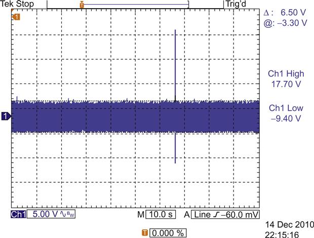
The oscilloscope trace requires careful interpretation because it is preceded by 75 dB (≈×5,600) of AC coupled gain, so information can only be gleaned from edges, not DC levels. The trace shows a positive pulse due to a positive jump closely followed by a negative pulse due to a negative jump. As measured by the oscilloscope, the amplitude of the positive pulse is 17.7 V, but as the NE5532 op-amp preceding it has ±18 V rails, it can be assumed that it was clipped and that the original jump exceeded 3.2 mV. However, the negative step at −9.4 V would not have been clipped, and as the oscilloscope was in ‘peak detect’ mode, its amplitude can be assumed to be correctly captured at −1.7 mV. Summarising, the burning voltage jumped up by >3.2 mV and almost immediately fell back by 1.7 mV to a new slightly higher burning voltage than before the two jumps.
Maximum stability is achieved by stabilising the valve at the manufacturer’s preferred operating current, but if this current changes, even if it returns to its original value, the valve takes time to recover its original stability.
Although a gas reference may operate at 150 V, it needs extra energy to strike the glow discharge. There are three possible source of this extra energy:
• Provide a sufficiently high (current limited) striking voltage. (Mullard 150C4 in total darkness needs 225 V.)
• Allow the photons in the ambient light to provide the extra energy. (Mullard 150C4 striking voltage drops to 185 V.)
• Add a radioactive gas such as 85Kr that emits beta particles (electrons) having an average energy of 200 keV.
The significance of these three sources is that if the last two are not available, a gas reference may require a higher striking voltage than expected. Krypton 85 has a half-life of only 10.756 years, so after 40 years it will have decayed to 7.6% of its original activity, significantly diminishing its striking assistance. Moral: Don’t rely on a manufacturer’s specified striking voltage if there’s any reason to think they used radioactive assistance to lower it. The GEC QS1215 90 V stabiliser’s data sheet states that an (unspecified) radioactive material is used to maintain the same maximum striking voltage (115 V) irrespective of light or darkness, but the Mullard 90C1 has similar specifications with no mention of radioactivity. Despite these theoretical caveats, the author’s sole QS1215 only needed a striking voltage of 107.13 V in total darkness – well within specification.
Optimised Valve Voltage Regulators
Oscilloscope design presents many challenges because a bandwidth of DC to at least 20 MHz is required. Valve oscilloscopes required stable, quiet HT supplies, so their voltage regulators were carefully optimised and heater voltages were stabilised against mains voltage variation by control circuits involving a saturable inductor in series with the mains winding of the heater transformer [17].
Any voltage regulator can be improved by increasing the gain of its error amplifier. A single triode has the lowest gain, but a pentode (or cascode) has higher gain. If even greater gain is required, a pair of stages can be cascaded (more than two stages would be impractical because phase shifts would almost certainly turn the regulator into a power oscillator). Because the error amplifier amplifies DC, drift must be minimised, so the first stage of a high-gain regulator must be a differential pair, and a dual triode is convenient. The second stage is much more flexible, and could be another triode differential pair, or a single-ended stage using either a triode or a pentode.
Using a Pentode’s g2 as an Input for Hum Cancellation
If a pentode is used as the second stage, g2 can be considered to be an inverting input. If the correct proportion of raw HT ripple could be injected at this point, it would cancel at the anode, resulting in a regulator with no hum at its output, but the tactic is not without its problems:
• For the pentode to operate correctly, g2 must be at the correct DC potential. This is usually derived from a potential divider across the (clean) output of the supply. A large-value resistor can then be connected from the raw HT, and its value adjusted until ripple is cancelled. The exact value of this resistor is awkward to calculate because we do not usually know the value of ![]() , so its value is usually determined by experiment. Values could be anywhere in the range from 150 kΩ to 1.5 MΩ.
, so its value is usually determined by experiment. Values could be anywhere in the range from 150 kΩ to 1.5 MΩ.
• Although valve manufacturers specified most parameters quite tightly, we now rely on an unspecified parameter, and there is no guarantee that valves made by different manufacturers that meet all the specified parameters will match our unspecified parameter. As an example of this problem, the 1970s four-tube EMI2001 colour camera set beam current by controlling g2, so whenever a new tube was ordered (£1500 a shot in 1986), it was necessary to specify that the tube was to be used in an EMI2001 colour camera. Similarly, Tektronix stocked selected tubes (valves), not because they were better than any others, but because they were guaranteed to work correctly in their circuit.
• Variations between valves mean that the cancellation is not perfect, but any remaining ripple is easily mopped up by the loop gain of the error amplifier.
Increasing Output Current Cheaply
The majority of circuitry within oscilloscopes and audio is Class A, so it draws a very nearly constant current. One of the functions of a regulator is to regulate output voltage against changes in load current, but if the current is almost unchanging, much of the regulating ability is being wasted. As an example, the regulator might face a load with a quiescent current of 100 mA but that could rise to 150 mA, or drop to 50 mA under certain circumstances. We could design the regulator to be able to pass 150 mA, but this would need a bigger series pass valve. Instead, we could bypass the series pass valve with a resistor that allowed 50 mA to flow directly into the load. The series pass valve now only has to pass 100 mA under full load. When the load requires only 50 mA, this is provided entirely by the bypass resistor, and the regulator is in danger of dropping out of regulation, so this condition sets the limit for the maximum current that may be bypassed by a resistor.
Adding the bypass resistor slightly increases ripple because it injects raw HT into the clean circuit, but because the output resistance of the regulator is likely to be <1 Ω, potential divider action greatly reduces the added ripple. As an example, the following circuit incorporates both of these modifications (see Figure 5.47). The regulator showcases some other tricks that improve performance.
As previously mentioned, gas references produce noise, but because we have chosen to use a differential pair, the gas reference now drives a high-impedance input, so we can add a filter to reduce noise. The capacitor previously across the reference has been removed because of the danger of it causing oscillation when excited by voltage jumps (this was previously damped by rk of the valve). Additionally, the current through the gas reference has been stabilised at the manufacturer’s preferred operating current, so jumps should be minimal.
The ECC83 differential pair has its anodes at 209 V, and although it would just be possible to directly couple this voltage to the grid of the EF91 pentode, its cathode would be at ≈213 V, which would not only cause problems with Vhk, but would reduce gain because of the necessarily high value of Rk. To reduce this problem, Vk has been reduced to a similar voltage to the cathodes of the ECC83, allowing them to share a heater supply. We could simply insert a cathode resistor to ground, but a potential divider across the regulated output can set the required voltage and give a much lower Thévenin output resistance (15 kΩ versus 800 kΩ). The significance of this resistance is that it reduces the gain of the stage, so we want as small a resistance as possible to maintain maximum open-loop gain in the regulator.
To couple an anode of the ECC83 to the EF91, a potential divider is needed to drop the voltage from 209 V to 90 V, thus we sacrifice ≈7 dB of DC open-loop gain. However, the sacrifice is worthwhile because gain is recovered faster by dropping Vk (and reducing local feedback) on the EF91 than it is lost by the potential divider. Ultimately, the choice of Vk is usually determined by Vhk considerations. Nevertheless, we could recover the gain at AC by bypassing the upper resistor with a capacitor, although we would need to check that the circuit was still stable.
The ECC83 differential pair has a constant current sink tail. If we were making symmetrical split rail supplies, we could simply take a large tail resistor to the negative supply, but a single supply needs the constant current sink.
Finally, because of the greatly increased open-loop gain, the regulator has a much lower output DC resistance than before (<10 mΩ), so it needs a commensurately large bypass capacitor to maintain low output impedance at higher frequencies. The author’s recent capacitor measurements show that only plastic capacitors have a sufficiently low ESR to shunt 10 mΩ, but 120 μF 400 V plastic capacitors are bulky and expensive.
As can be seen, much can be done to improve the basic valve voltage regulator, but the penalty is considerable cost and complexity.
Regulator Sound
Single-ended amplifiers (whether pre-amplifiers or power amplifiers) supplied from a regulator force the error amplifier to track the musical waveform. This is because the amplifier draws a current proportional to the music, and the regulator’s error amplifier strives to maintain a constant voltage in the face of this changing current. At high frequencies, the output shunt capacitor is a short-circuit and maintains a low output impedance, but at low frequencies it is the error amplifier that must do the work and cope with the (musical) current waveform. The quality of the regulator is therefore inevitably audible. Nevertheless, regulator defects are still an order of magnitude below passive supply defects.
Power Supply Output Resistance and Stereo Crosstalk
In Chapter 2, we designed simple stages and made the explicit assumption that our power supply had zero output resistance at all frequencies from DC to light. Feedback regulators have low, but not zero, output resistance, so this parameter is often specified. As examples of typical 300 V regulators at low frequencies, a well-implemented simple valve regulator can achieve ≈2 Ω, an optimised valve regulator ≈10 mΩ and a typical Maida regulator ≈80 mΩ.
The question is, how important is power supply output resistance? Or, more specifically, how high can it be before it becomes a problem? All gain stages use their load resistance RL to convert a change of signal current into a signal voltage. If the power supply has AC output resistance rsupply, then this resistance is in series with RL and slightly increases the gain of the stage:
If we first assume that rsupply is constant with frequency, then there’s no problem for a single stage. However, if we share this supply between a pair of stereo channels, the signal current of one channel’s stage crosstalks into the other, via a pair of potential dividers (see Figure 5.48).

Rigorous calculation of this cascade of potential dividers is unnecessary because we know rsupply must be quite small, so we simply determine individual potential divider attenuations, and then multiply them together. As an example, a stereo pair of common cathode E88CC stages might have RL=33 kΩ, ra=6.6 kΩ and rsupply=2 Ω:
Crosstalk at −100 dB is certainly adequately low, but if we increase rsupply to 200 Ω, crosstalk deteriorates to −60 dB, which although perfectly acceptable for an RIAA stage (cartridge crosstalk rarely exceeds −35 dB, even in the mid-band) would undoubtedly be criticised elsewhere despite the fact that a 26 dB difference in level is sufficient to slew the apparent position of the source firmly to one loudspeaker.
However, we should note that because the factor RL appears in both denominators, the most effective way of reducing stereo crosstalk is by maximising RL, rather than minimising rsupply. Note also that rsupply is likely to be inductive due to falling regulator error amplifier gain with frequency, implying crosstalk that deteriorates with frequency.
Power Supply Output Resistance and Amplifier Stability
When we calculated stereo crosstalk, the second potential divider described how well the stage could reject a signal from the power supply, so it was the Power Supply Rejection Ratio (PSRR) term we first saw in Chapter 2, whereas the first potential divider described how well the power supply could attenuate an injected signal. Whenever individual stages are interconnected to form a system, each stage requires power, which must ultimately be derived from a common source (even if that common supply is the AC mains entering the building). Thus, the stereo crosstalk concept can be extended to include coupling between two entirely different stages via the power supply.
The significance of common power supply coupling between two entirely different stages is that one might be the input to the other, so if the output of the second is coupled to the first via the common power supply there might be sufficient loop gain and phase shift to allow oscillation. If the common power supply had zero output resistance, there could be no coupling, but this is not possible. Moreover, the common power supply is unlikely to have a constant resistance and is more likely to have a complex impedance that changes with frequency.
Traditional electronics used an RC ladder network as a means of progressively attenuating power supply ripple from the (less sensitive) output stage to the (most sensitive) input stage. The smoothing capacitors are an open circuit at very low frequencies, so they no longer effectively attenuate power supply coupling from the output stage back to the input stage, and if there is enough low-frequency gain in the amplifier, the system can become a blocking oscillator [18]. This low-frequency (≈1 Hz) phenomenon was known classically as motorboating, but marginal stability probably went unnoticed much of the time, because loudspeakers of the time had very stiff suspensions and their cones were rarely visible. The fault was in the power supply, yet the traditional ‘cure’ was to reduce the value of one of the amplifier’s coupling capacitors.
Rather than having an RC ladder network, we could connect all the stages to a single regulator. Provided that the regulator has zero output resistance, there can be no coupling from one stage to another via the common power supply. In practice, a feedback regulator always has a complex output impedance that rises with frequency (hence the 2.7 mΩ+2.2 μH inductance of the 317) in order to maintain stability of its error amplifier. Thus, a feedback regulator has low enough output impedance at low frequencies to prevent motorboating, but its rising impedance at high frequencies might allow the circuit it powers to burst into high frequency oscillation instead.
A guaranteed way of breaking the loop is to add a regulator per stage because this adds the PSRR of each regulator (typically 60 dB) to the PSRR of the stage (anywhere between 0 dB and 60 dB). Solid-state electronics could cheerfully add a ±15 V regulator to each stage at minimal cost, but HT regulators are more difficult; a clutch of Maida regulators would be a significant investment, and the idea of multiple valve regulators is mindboggling (although that didn’t stop Glen Croft in 1984). Thus, we need something cheap, simple and robust.
The Statistical Regulator
This circuit acquired its name because it applies simple statistical rules in a novel way, resulting in a simple regulator producing extremely low noise and having very high ripple rejection.
As we saw earlier, all regulators are based on the potential divider; series regulators control the upper arm and shunt regulators the lower arm. It’s a good engineering maxim that if a large improvement is needed, it’s easier to obtain it in a number of small bites than one large one. We have to work hard to achieve 80 dB of attenuation in a single regulator, but obtaining two attenuations of 40 dB is easy. Thus, we could cascade regulators in the same way that Scroggie showed that cascaded filters achieved high attenuation more efficiently than a single brute force filter, but this multiplies the drop-out voltage by the number of regulators. What would be better would be to make a regulator that controls both arms of the potential divider simultaneously. The individual arms need not be especially good because their combination would make a very good regulator.
It is probably possible to make an adjustable high voltage regulator having a feedback loop controlling series and shunt elements simultaneously that doesn’t explode at switch-on. Whether it would be stable when connected to a real load is another matter. Fortunately, we won’t need our regulator to be adjustable because we will know the exact voltage and current required. Thus, we do not need a potentially unstable control loop – we could optimise the two arms independently and run them open-loop.
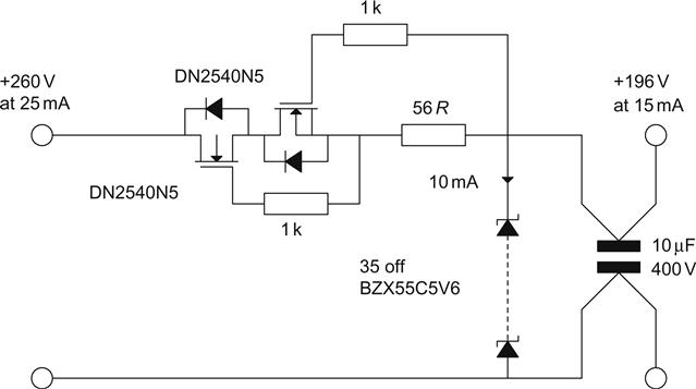
The ideal upper arm would have infinite slope resistance, whereas the ideal lower arm would have zero slope resistance. We saw in Chapter 2 that we could make a very good constant current sink using two DN2540N5s and three resistors, so this would make an excellent (and simple) upper arm. The lower arm needs to be a constant voltage and at its very simplest could be a string of gas references or Zener diodes (see Figure 5.49).
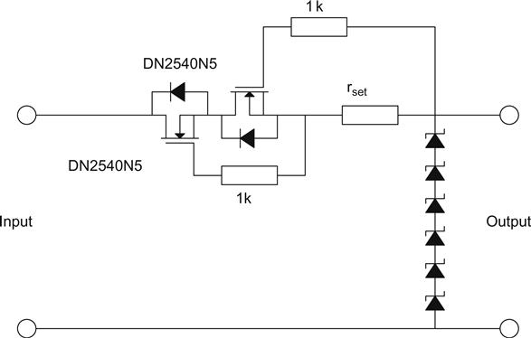
Suppose a load needed 195 V at 15 mA. To allow for signal variation in load current and to ensure that the voltage references operate correctly, the lower arm should pass a minimum of 10 mA. Thus, the constant current sink must be designed to pass 25 mA. Curve tracer measurements of a DN2540N5 at 25 mA and 100 V suggested gm≈148 mA/V and rds≈41 k, resulting in μ≈6,000. For that particular device, Vgs for 25 mA≈1.45 V, so a 56 Ω programming resistor would be needed. The cascode constant current sink multiplies the value of its programming resistor by the product of both μ, but the lower DN2540N5 is forced to operate at a very low voltage, badly compromising both gm and rds, drastically reducing μ. Careful AC measurement suggested rslope≈30 MΩ with an uncertainty of ±12% for a DN2540N5 cascode constant current source set to 25 mA.
Suppose that the lower arm was a series chain of Zener diodes. We saw in Chapter 3 that a composite device made of multiple 5.6 V Zeners was particularly quiet. To achieve 195 V (actually 196 V), we would need 35 diodes, and a total slope resistance of ≈400 Ω at 10 mA is likely.
We can now use the potential divider equation to determine the attenuation caused by the constant current sink and Zener string:
97 dB is a very impressive attenuation, although it will vary considerably between different samples of DN2540N5s and improve substantially as current increases (Zener slope resistance falls with current whilst JFET gm rises). Nevertheless, such a satisfyingly large number means we need not determine it accurately, we can just assume that it will be ‘good enough’ and turn our attenuation to practicalities.
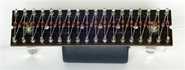
Thirty-five 5.6 V Zener diodes is a lot, and the knee-jerk reaction is to reject such a solution. However, a little more thought suggests that it is entirely practical, if a little unconventional. The primary disadvantage is not cost (Zeners are cheap) but the tedium of soldering all those diodes in series (and every one the right way round). Zigzagging the diodes backwards and forwards across a tag strip is ideal because despite the fact that the total wire length of all 35 Zeners on the author’s tag strip ≈680 mm, and has a calculated ≈1 μH series inductance, its time constant of 5 ns is insignificant (see Figure 5.50).
Short-circuiting the output of the regulator puts the entire input voltage across the DN2540N5 cascode. Surprisingly, the author’s prototype regulator survived this inadvertent abuse, but it is essential that the upper DN2540N5 has an adequate heatsink to cope with the short-circuit dissipation.
Shunt regulators also run the risk of self-immolation if their load is removed because this forces the shunt element to dissipate the design current plus load current. Both the BZX55 and the BZX79 series are rated at 500 mW, so for a 5.6 V diode that means a maximum current of 89 mA.
Bypassing the Composite Zener
Although the composite Zener produced very low noise measured over a 22 Hz to 22 kHz bandwidth, it produced 20 dB more when this filter was removed, which was a larger increase than initially expected, and the culprit is mains interference via the 12 pF output capacitance COSS of the DN2540N5. If we assume a slope resistance of 30 MΩ for the cascode constant current source (CCS) and 400 Ω slope resistance for the 195 V composite Zener, we can draw a diagram (see Figure 5.51).

Looking at the diagram, we observe that COSS short-circuits the 30 MΩ slope resistance, and if we calculate their time constant (360 μs) this implies that mains noise rejection falls at 6 dB/octave from 442 Hz upwards. The solution is to convert the circuit into an oscilloscope probe by adding a 0.9 μF capacitor across the lower resistance to form another 360 μs time constant. Our potential divider now has equal time constants top and bottom, implying constant 97 dB attenuation with frequency. In practice, the 12 pF COSS estimate is likely to be unreliable, but the calculation gives us a useful lower bound to the required value of bypass capacitor, and 4.7 μF would ensure that attenuation did not deteriorate as frequency rose. Since the entire circuit is reasonably simple, it was possible to make a model including Zener and capacitor series inductance and resistance, and drive it from COSS in parallel with 30 MΩ to simulate the cascode CCS (see Figure 5.52).
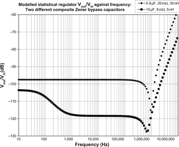
As expected, the 0.9 μF capacitor allows constant attenuation with frequency, and the 1 μH series inductance (due to wire length) of the composite Zener is irrelevant. As with the LC filter, the value of bypass capacitance determines the depth of the attenuation plateau, its ESR nulls depth at the capacitor’s self-resonant frequency, and its series inductance determines behaviour above self-resonance. The model compares a typical 0.9 μF plastic capacitor having ≈15 mm tails at each end with a 10 μF polypropylene capacitor having a four-wire Kelvin connection that renders tail inductance irrelevant. We now have a complete set of component values for our supply (see Figure 5.53).
As can be seen, the statistical regulator is very simple, yet measurements show that it is extremely good. Even better, it occupies little space so it can be positioned at the optimum point – adjacent to the load. Since it is best suited to pre-amplifiers, it is best to site the raw supply (transformer, rectifier, smoothing) remotely.
Optimising the Statistical Regulator
It is an engineering rule of thumb that Zeners should operate at a current of 10 mA or more (see Figure 5.54).
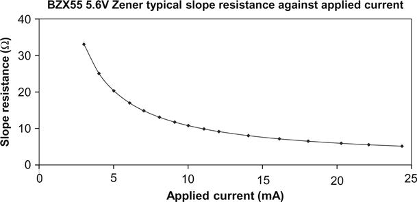
The graph was produced by measuring Zener voltage against applied current for the composite 195 V Zener, fitting an equation of the form V=a·ln(I)+b·I to the curve, differentiating that equation to produce a slope resistance equation and dividing its coefficients by the number of individual Zeners. The graph is therefore an average of 35 BZX55 5.6 V Zeners from one batch, and although exact coefficients may vary from one batch to another, the general trend will remain. The slope resistance of the author’s batch of BZX55 5.6 V Zeners could be found from:
Thus, slope resistance falls from 20 Ω at 5 mA to 11 Ω at 10 mA and 6 Ω at 20 mA. The 1.2 Ω constant is probably the resistance of the fine wires needed to connect to the silicon die.
The DN2540N5 is a power JFET, and its gm at low currents (<10 mA) is quite poor, significantly reducing the slope resistance of the cascode CCS, so it should pass a minimum current of 20 mA.
We saw in Chapter 3 that the noise generated by a DC reference was inversely proportional to the square root of applied current. Thus, although 10 mA of Zener current is sufficient to obtain a usefully low Zener slope resistance, doubling to 20 mA reduces Zener noise voltage by 3 dB. Since the current rating of the composite Zener is a constant 89 mA (500 mW/5.6 V) irrespective of total voltage, 20 mA is perfectly tenable, leaving 69 mA for load current. It would be wasteful to sink 20 mA of Zener current just to provide 1 mA of load current, so this implies that the statistical regulator is best suited to load currents of between 20 mA and 70 mA.
References for Elevated Heater Supplies – the THINGY
An elevated LT supply is required for any circuit having a cathode significantly above 0 V because leakage currents from heater to cathode Rhk(hot) otherwise develop a noise voltage across the AC resistance seen looking into the cathode.
There are two ways of reducing the leakage current and therefore noise voltage:
• Don’t use valves with poor Rhk(hot). A valve tester or purpose-made jig can be used to select good examples. Because the most common cause of poor Rhk(hot) is fluff or dust contamination during construction, it can often be burnt off by increasing heater volts by 2/3 and monitoring Rhk(hot) without drawing any anode current. The resistance will begin to fall, and the moment it stops changing, switch the heater off, and allow the heater to cool. With luck, when tested again, Rhk(hot) will be significantly improved. Note that raising the heater voltage easily damages an oxide-coated cathode, but if the valve was unacceptable anyway, you have nothing to lose.
• If the DC voltage across the leaky insulation was zero, the leakage current would be zero, and so would the noise.
In this example, it has been assumed that there are two heater supplies: one for valves with cathodes at ≈0 V and the other for valves with cathodes at ≈130 V, so if we were to follow the RCA recommendation, we would require heaters elevated by +40 V and +170 V. Although these voltages will not supply any current, they need a reasonably low AC source resistance and adequate filtering (see Figure 5.55).
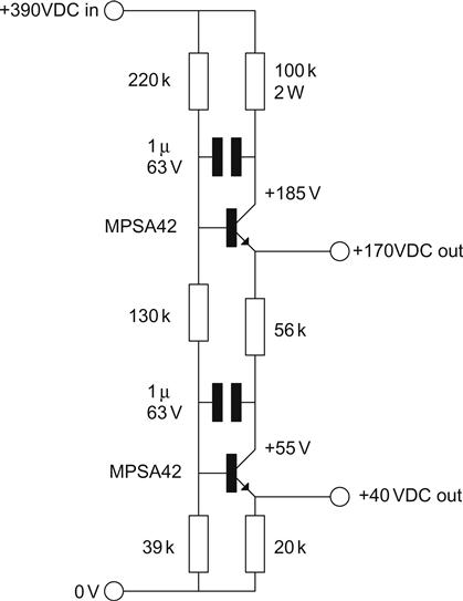
The circuit is connected across the output of the HT supply, and it is a pair of emitter followers whose output voltage is set by a tapped potential divider. The circuit is utterly non-critical of component values and is easy to design/modify. Since we are dealing with reasonably high voltages, we will neglect Vbe and consider the output voltages to be the same as the voltages at the tappings of the potential divider. If we neglect base current and arbitrarily set the current passing down the potential divider to 1 mA, then each resistor drops 1 V per 1 kΩ of resistance. Thus, if we want 40 V at the lower output, then 39 kΩ will be near enough for the lowest resistor. If the upper output is to be at 170 V, then the drop across the middle resistor is 170 V−40 V=130 V, and a 130 kΩ resistor will do nicely. If the HT voltage is 390 V, then the upper resistor must drop 390 V−170 V=220 V, so a 220 kΩ resistor is required.
Although the circuit only applies a potential to the external circuit, and does not source any current, each transistor must pass some collector current, but this current is not critical, and anywhere between 1 mA and 2 mA is fine. If we set Ic=2 mA, then the emitter resistor of the lowest transistor needs to be 40 V/2 mA=20 kΩ.
We could connect the collector of this transistor directly to the emitter of the upper transistor, but adding a collector load resistor improves the circuit’s noise rejection and reduces power dissipation in the transistor. The resistor value is not in the least critical, but if we set Vce=15 V for the lower transistor, then its collector must be at 40 V+15 V=55 V. The emitter of the upper transistor is at 170 V, so the voltage across the collector load resistor must be 170 V−55 V=115 V. Since the resistor passes 2 mA, its resistance must be 115 V/2 mA, and 56 kΩ is quite close enough. The advantage of including the collector load resistor is that it reduces Vce (which reduces dissipation) and improves filtering.
The upper transistor also needs a collector load resistor. If we again assume Vce=15 V, the collector of the upper transistor must be at 170 V+15 V=185 V. The HT is 390 V, so the upper collector load resistor drops 390 V−185 V=205 V. It passes 2 mA, so its resistance is 205 V/2 mA, and a 100 kΩ resistor will do nicely. 205 V across a 100 kΩ resistor dissipates 0.42 W, so a 2 W component is required.
Filtering is achieved by placing the filter capacitor not from base to ground, which would require a high voltage component, but from base to collector. For the lowest transistor, gain to the collector Av=−RC/RE=56 kΩ/20 kΩ=−2.8, and the Miller effect therefore multiplies this capacitor by a factor of 3.8, so the effective value is 3.8 μF. Input resistance at the base of the transistors is approximately the Thévenin output resistance of the resistor chain, and the filter cut-off frequency is therefore 1.5 Hz. The lower emitter follower sees two cascaded 1.5 Hz filters, so noise is further rejected. The value of capacitance is not the least critical.
There is no reason to stop at just two outputs; extra output voltages can easily be derived by cascading more sections. Each section adds extra filtering, so you might choose to add a section just to improve noise rejection. Output resistance is less than 2 kΩ, although supplementing each transistor with another, to form a Darlington pair, would lower this output resistance.
The author was stumped for some time in attempting to name this circuit, but eventually realised that it is a Transistorised Heater Insulation Noise Grounding Yoke (THINGY), which is what people have been calling it anyway.
Note that all of the circuitry within an elevated LT supply is at least at the elevated voltage and that it therefore represents a shock hazard if touched. Even though the circuitry only contains components rated at a low voltage, elevated supplies should be treated with as much caution as HT supplies.
Common-Mode Interference
All of the previous discussion (rectification, smoothing/filtering, regulation) has been concerned with producing a source of DC power between two terminals with as little noise or interference as possible, and although not explicitly stated, this was differential-mode noise and interference. In this section, we will investigate common-mode interference where the difference in voltage between the supply’s terminals may well be zero but both terminals are bouncing up and down in unison with respect to earth.
Common-mode interference often passes unnoticed. The problem becomes apparent when not only is common-mode interference present, but there is a mechanism for converting it into differential-mode.
Heaters and History
Golden age pre-amplifiers had AC heaters and suffered hum by modern standards. Sometimes this was due to leaky heater/cathode insulation, but mostly it was due to capacitance between heater wiring and signal wiring. The first solution was to centre tap the heater supply so that the heater wires had equal and opposite voltages, then to tightly twist the heater wiring. In this way, although there was capacitance from each heater wire to a given sensitive point, provided the twist was tight enough the two capacitances were equal (balanced), so the interfering currents cancelled. Because there’s a practical limit to how tight the twist can be, the two capacitances cannot be perfectly equal, but provided that capacitances were minimised by pushing heater wiring into the corners of the chassis and only bringing it up to the valve at the last moment, the imbalance capacitance that caused hum was minimised.
The next step was to replace AC heater supplies with DC, and this produced an immediate measurable improvement in 50-Hz or 60-Hz hum that was often essential in microphone amplifiers. Remembering that the coupling mechanism to the signal electronics is capacitive, high frequencies will be coupled more easily, and rectification produces a spray of high-order harmonics of mains frequency. DC heater supplies need careful filtering if they are not to substitute a rattling buzz for the original hum; a simple rectifier and large reservoir capacitor are not sufficient.
Filtering low-voltage, high-current supplies was expensive in the 1950s, so the problem was eased by a low current heater variant of the input valve (UF86 needs 100 mA at 12.6 V as opposed to the functionally identical EF86 needing 6.3 V at 200 mA). A tape recorder of sufficient quality to require a low-hum microphone amplifier probably had a push–pull loudspeaker amplifier that drew ≈100 mA from its HT supply, so a common trick was to power the UF86 from the HT supply return. The rarer, more expensive solution was to provide a dedicated heater supply with CRC filtering.
Any three-terminal IC regulator added after a rectifier and reservoir capacitor produces a close enough approximation to DC that differential-mode interference from heater wiring is eliminated.
How Common-Mode Heater Interference Enters the Audio Signal
Common-mode heater interference is a problem for small-signal valves because the interference current is coupled from the heater directly to the enclosing cathode via Chk (and Rhk if it is poor). The interference current develops a noise voltage across the cathode impedance rk//Zk, which appears as a signal at the cathode, is summed with the wanted signal and amplified by the valve. There are two distinct scenarios:
• In a single-ended stage, the cathode will be (should be) coupled to ground via a low AC impedance Zk. This low impedance might be the slope resistance of an LED or a large capacitor. But neither component can bond the cathode emissive surface directly to earth, so the non-zero length of the wiring has inductance which reduces coupling at RF, as does diode slope resistance, capacitor ESR and wiring resistance.
• In a differential pair, the cathode unavoidably has quite a high resistance to ground (via the anode load resistors divided by the μ of the valve – not the cathode resistance) and cannot form a useful CR filter in conjunction with Chk. We are forced to rely on the (usually quite poor) RF balance of the differential pair to reject RF, so a differential pair is likely to be more sensitive to heater-borne interference than a single-ended stage.
Mains Transformers and Inter-Winding Capacitance
Since we cannot remove the path within the valve for coupling common-mode interference from the heater supply to the audio signal, we must prevent common-mode interference from reaching the heater supply.
A typical mains transformer has 1 nF of capacitance between adjacent windings, so rather than a spike being stepped up or down by the winding ratio, it is coupled unattenuated via this capacitance. Thus, a 1 V voltage spike that is an insignificant proportion of the 300 V HT can be coupled to a 6.3 V winding where it is very significant. HT rectifier diodes inevitably generate spikes when they switch, and the author has observed HT switching spikes on the 6.3 VAC LT supply of a Leak Stereo 20 chassis due to inter-winding capacitance in the shared mains transformer.
Sensitive heater supplies require a separate transformer from high-voltage rectification (HT supplies, HT rectifier heaters and bias supplies).
Reducing Transformer Inter-Winding Capacitance
The capacitance of a parallel plate capacitor is directly proportional to the area of the plates and inversely proportional to the distance separating them, so if we could reduce the area between the primary and secondary and increase their separation, we would reduce the inter-winding capacitance. (The effect of attempting to adjust the dielectric constant would be minimal.)
As an example, the Maplin 100 VA EI transformer kit is of split bobbin construction with the primary wound in one half of the bobbin and the other half left empty for the user to wind the secondary. The area of the inter-winding capacitor on a split bobbin transformer is simply the area of the divider between primary and secondary less a little at the corners because the copper windings tend to curve as they bend round each corner (see Figure 5.56).
The capacitive area of the divider is ≈1,800 mm2. Conversely, if the divider was to be removed and the bobbin filled with layer-wound windings, the area between the primary and secondary would be ≈7,200 mm2, increasing the capacitance by a factor of 7,200/1,800=4.
Turning to the thickness between the plates, a typical polyester transformer insulation tape might be 0.055 mm thick, but although a single thickness would theoretically be rated at 3 kV breakdown voltage, a transformer manufacturer would be aware that practicalities could require four layers of this tape between the primary and secondary layers to guarantee adequate dielectric strength to adequately insulate mains voltages, giving a total inter-winding thickness of 0.22 mm. Conversely, the divider in the split bobbin transformer is 1.07 mm thick, so it reduces capacitance by a factor of 1.07/0.22=4.9.
Taken together, the reduced plate area and increased separation of the example split bobbin transformer reduce inter-winding capacitance by a factor of 4×4.9≈19.5, implying an interference reduction of ≈26 dB.
Before mains-borne interference can reach the inter-winding capacitance, it must pass through the transformer’s leakage inductance, so these two components form a resonant network. If we assume (for the purposes of comparison) that the resulting current develops a voltage across a 1 Ω earth bond resistance between the heater winding and the chassis, we can model the three main transformer constructions. The author measured the leakage inductance and primary to secondary interwinding capacitance of three commercial 100 VA transformers, and then modelled how well common-mode interference transferred to the resistance (see Figure 5.57).
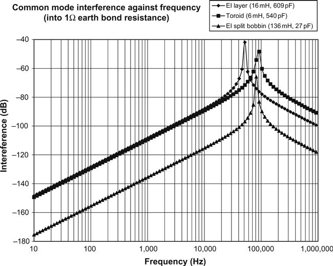
Surprisingly, the large differences in leakage inductance are immaterial, and interference at audio frequencies is determined purely by inter-winding capacitance, with the split bobbin example passing 27 dB less interference than the layer wound or toroid.
Post-Transformer Filtering
We have seen that segregating HT and heater transformers and choosing split bobbin construction (mandatory in Australia) reduce common-mode interference but further filtering may be necessary.
Even if a 6.3 V heater winding already has a centre tap, we can add a very cheap LR filter simply by connecting a 47 Ω resistor from each end of the winding to chassis – the filter uses the leakage inductance of the transformer.
We can make an explicit common-mode filter by adding series inductance to each leg of the heater supply and capacitance from each leg to the chassis. Since we are trying to filter common-mode noise, rather than differential-mode, we wind a bifilar choke on a small ferrite core and do not worry about core saturation because the currents in the two coils create equal and opposite fields, which cancel, so the core does not see any net magnetisation. Commercially made common-mode chokes are readily available.
Practical Issues
Although we now have enough theory to determine component values and ratings in each of a power supply’s individual blocks, there are some practical considerations that should be addressed before we design a complete supply.
Transformer Regulation
Transformer manufacturers quote secondary voltage at rated current and also regulation as a percentage:
A typical 50 VA transformer might have a regulation of 13%, so a 6 V 50 VA transformer could be expected to produce 1.13×6 V=6.78 V off-load, and this is the voltage PSUD2 needs.
Perhaps more significantly, if we need 6.3 V, we can achieve it by under-running a 6 V transformer. We start by rearranging the previous equation:
We now say that rather than using the entire current rating, we will use a fraction of it:
Thus, for our 50-VA 6-V example, the full-load current would be 8.33 A, but if we only needed 4 A, our current fraction would be 4 A/8.33 A=0.48, so:
Thus, we can achieve 6.3 V from a standard 6 V transformer and have 80 mV in hand for voltage drop across the heater wiring. This trick of using an oversized standard transformer can be a very useful way of avoiding the expense of a custom-wound transformer.
HT Capacitors and Voltage Ratings
The capacitors for 300 V HT supplies are easily obtained because the switched mode supplies in computers need 385 V capacitors to cope with the 340 V resulting from rectifying 240 V mains. But if we need a higher HT voltage, perhaps 430 V for a pair of EL34s, then a 450 V rated capacitor would be overstressed if mains voltage rose by 6% (as it is legally allowed to do). There are two choices: we either use a higher voltage capacitor, which will usually be paper or plastic film and generally only available in quite low values, or connect ‘n’ equal-value electrolytic capacitors in series to obtain a composite capacitor having a total voltage rating multiplied by ‘n’ but total capacitance divided by ‘n’.
Because the capacitors are connected in series, the current passing through the capacitors must be equal, so each capacitor receives an identical charge (Q=It). If their capacitances are equal, then the voltage across each one of them must be equal (Q=CV).
Unfortunately, even if the capacitances are equal, the leakage currents in each individual electrolytic capacitor are unlikely to be equal, so the voltage across each capacitor will not be equal. To equalise the voltages, and prevent one capacitor from exceeding its rated voltage, each capacitor should be bypassed by a resistor so that the resulting potential divider chain forces the voltages to be equal (see Figure 5.58).
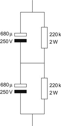
The divider chain should pass at least 10 times the expected leakage current of the capacitors to ensure correct operation. Typically, a 220 kΩ 2 W resistor suffices.
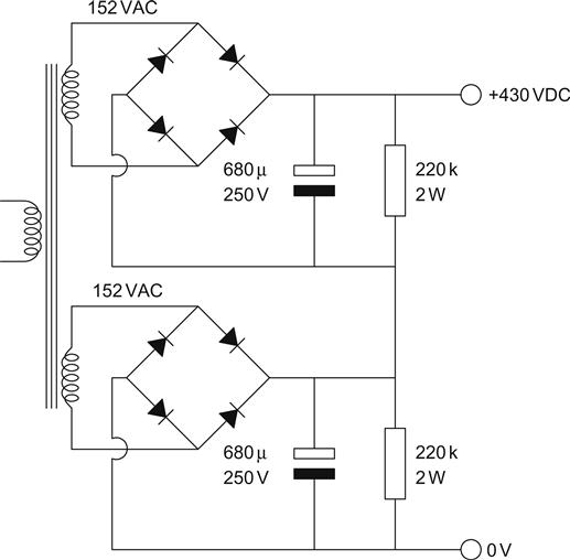
A technically better method is to use separate HT windings and rectifier/smoothing circuits, and place the resulting floating DC outputs in series to obtain the required HT voltage. This ensures that each capacitor cannot exceed its rated voltage, but the mains transformer is now more complex (read expensive) (see Figure 5.59).
Can Potentials and Undischarged HT Capacitors
Both of the previous schemes for producing a composite HT capacitor of high voltage rating resulted in one capacitor with its negative terminal stood away from ground potential. This is significant because the can of an electrolytic capacitor is connected either to the negative terminal or at a potential very close to it. Cans at an elevated voltage must not only be insulated from the chassis (flanged plastic capacitor clamps that prevent the can touching the chassis are therefore best), but the capacitor must also be properly insulated from the user.
HT supplies represent a formidable shock hazard, and it is essential that provision is made for fully discharging the reservoir and smoothing capacitors when the equipment is switched off. The HT supply therefore needs a purely resistive discharge path to 0 V at some point, and the simplest way of providing this is to connect a 220 kΩ 2 W resistor across the reservoir electrolytic, which not only discharges the capacitor, but also (provided that there is a return path) discharges subsequent HT capacitors.
The Switch-On Surge
If we do not use a valve rectifier, the HT switches on instantly, and suddenly applying 400 V to an electrolytic capacitor stresses both dielectric and electrolyte, so we should look to see if there is some way of prolonging life. (Given that computers typically last only five years before being consigned to landfill, physical longevity of their power supplies is scarcely an issue, so they don’t worry much about switch-on transients.)
When we apply rectified AC to the reservoir capacitor, we may be unlucky enough to switch at the instant that the cycle is at its peak voltage. The instantaneous transition from 0 V to 325 V (dV/dt ≈∞) applied to the capacitor causes a theoretically infinite current to flow because:
If, however, we could always switch at the zero-voltage point, then although dV/dt for a sine wave is at a maximum at this point, it is not infinite, and the inrush current is reduced. Devices capable of performing this switching are known, predictably, as zero-voltage-switching relays and the Crystal Palace amplifier in Chapter 6 uses one to soften the inrush to its main HT supply.
However, the author is beginning to harbour suspicions that these relays might cause switching spikes as the mains crosses 0 V and switching is handed between the two back-to-back thyristors that make up the internal triac, and he’s certainly seen some odd effects on logic lines as a zero-voltage-switching relay switched an inductive load, so in low-noise applications perhaps it’s time to revert to hard vacuum rectifiers and simply switch mains to the HT transformer (that also has the rectifier heater winding) using a conventional switch or electromechanical relay.
Mains Fusing
Although UK mains plugs have a fuse in the line, it’s there to protect the lead, not the equipment.
The first component the line should meet when it enters a piece of equipment is an appropriately sized fuse that protects against fire in the event of an over-current fault within that equipment. If we use one piece of equipment to switch and distribute mains to other equipment, we must fuse its internal electronics separately from the mains distribution. 230 V appliances in North America require double-pole fusing (a fuse in each line) because the 230 V is actually a two-phase system of 115 V–0–115 V (centre tap to earth), so although a single fuse would protect against an over-current fault from line to line, each line must be protected against line to earth faults.
Fuses are manufactured to be ‘fast’ (F) or ‘timed’ (T). ‘Timed’ used to be called ‘anti-surge’, and these fuses are intended to survive a short inrush current considerably higher than their sustained current rating. Almost all electronic equipment draws an inrush current at switch-on as reservoir capacitors are charged or toroidal transformers kick, so we always need ‘timed’ fuses, but how do we determine their rating?
Fuse manufacturers’ data sheets have plenty of graphs that refer to I2t ratings. What they’re pointing out is that if a fuse wire has a certain mass, it must require a defined quantity of heat energy to raise its temperature to melting point so that it ruptures. Recall that power=I2R and that energy=Pt, and I2t ratings suddenly make sense. At this point, the hopeful author reached for his Hall effect current probe, used his digital oscilloscope in ‘single sequence’ mode to capture a mains inrush current at switch-on, set the oscilloscope’s ‘math’ function to Ch1×Ch1 (to give I2), positioned cursors at the beginning and end of the pulse, gated a ‘mean’ measurement on ‘math’ by the cursors, and then manually multiplied that mean value by the time between the cursors to arrive at an accurately measured value of I2t.
Unfortunately, further reading of fuse data sheet reveals what we already knew subliminally. Fuses aren’t terribly accurate, and as their I2t rating falls closer to the measured value, we’re more and more likely to suffer nuisance blowing. Understandably, fuse manufacturers express the situation more formally in terms of probabilities, but their advice amounts to: Guess/measure an I2t rating, try a fuse of that rating and if it blows too often without there being a fault, try the next current rating up.
Mains Switching
Mains switching is similar to mains fusing but may have a complication added by the incoming mains connector.
For a single phase system, a single switch in the line conductor is safest provided that connector polarity is unambiguous (IEC mains connector), but if the unpolarised two pin figure-of-eight small appliance connector is used, double pole switching (one switch in line and one in neutral) is necessary to ensure that no matter which way round the connector is inserted, line passes no further than the switch when in its ‘off’ position. Multiple phase systems (North American 230 V, German 380 V) are unlikely to be encountered in audio but would require switching of each phase.
It might be thought that a single phase system should be double pole switched irrespective of mains connector, but consider a piece of equipment having an earthed metal chassis, powered via an IEC connector, double pole switched, and imagine that the switch in the neutral fails open circuit. The equipment loses power and superficially appears safe for investigation to determine the fault. However, line is still present on the mains transformers and there is a very real danger of the investigator suffering a shock from line to the earthed metal chassis.
The easiest way to ensure safety of mains fusing and switching is to use an IEC inlet having an integral fuse and switch.
A relay allows remote mains switching. Thus, a low voltage switch on a control unit could energise a remote relay to switch mains. Unfortunately, that implies that we need permanently applied standby power in order to be able to switch the relay. The author was previously perfectly happy to leave RIAA-stage heaters permanently heated in standby mode, thus also providing power for the relay, but recent electricity price rises have changed that. Nevertheless, you might feel that the convenience of a relay outweighs the cost.
There’s a nasty little problem to be aware of in some relays. At its simplest, an electromechanical relay is just a coil of wire round a soft magnetic core that attracts a hinged soft magnetic material known as an armature to provide the switching action. A simpler (cheaper) relay can be made by passing the switching current through the armature, so when we switch our mains, we connect the relay’s (electrically conductive) core to 240 V. The core’s surrounding coil is wound on an insulating plastic former, so we have just connected a significant capacitance from one side of our heater supply to the mains – negating all our design efforts at reducing common-mode noise. Specify a relay withstand voltage of 10 kV, and the problem is unlikely to occur. The relays to be suspicious of have a low profile rather than being square when viewed from the side. If in doubt, reach for a hacksaw and sacrifice one to science to determine its exact construction before building that type in and having to diagnose the problem later.
A Practical Design
Having investigated individual blocks, we are now in a position to be able to design a complete HT and heater power supply. An RIAA stage imposes the most demanding power supply requirements, so we will design two variants of a power supply for this use; we can then add/discard/modify blocks as necessary for other applications.
The first variant is for the balanced hybrid RIAA stage of Chapter 7 that requires an HT of 195 V at 48 mA and a single heater supply of 6.3 V at 1.2 A. We will need:
We can now draw a block diagram (see Figure 5.60).
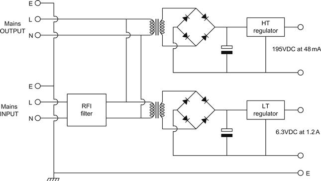
HT Regulation
There are three possibilities:
Valve regulators tend to be big. Techno-pretty, but big. An optimised valve regulator is bigger, prettier (even more glowing glass) and needs lots of heater supplies for all that glass. With care, an optimised valve regulator can achieve noise ≈1 mVpk–pk. The Maida regulator is small, doesn’t need heater supplies, but is electrically fragile, and produces noise comparable with a valve regulator but without the DC drift. The statistical regulator is slightly larger than the Maida regulator, but far quieter and more robust than the author expected.
The balanced hybrid RIAA stage uses a differential cascode input stage having limited PSRR, so the low noise of the statistical regulator makes it the natural choice (see Figure 5.61).
The cascode DN2540N5 CCS must be programmed to pass the load current plus the composite Zener current. The composite Zener could operate at 10 mA, but slope resistance and noise are significantly lower at 20 mA, so the CCS needs to be programmed for 68 mA. Field Effect Transistor (FET) device variation means that the required source programming resistance varies hugely, so a 50 Ω variable resistor is required – the 18 Ω resistor prevents accidental setting of excessive current. Although the programmed 68 mA current passes through both DN2540N5s, only the upper one has an appreciable voltage across it, so it will require a heatsink to dissipate 4–5 W, but we won’t know the exact power to be dissipated until we have designed our rectification and smoothing.
We know that we must use 5.6 V Zeners, so 195 V/5.6 V means that we need 35 of them in our composite Zener. Under normal conditions, the composite Zener passes 20 mA, but in the event of a catastrophic fault causing the entire load to be disconnected, the constant current source will drive its entire programming current of 68 mA down the composite Zener. Since each Zener is rated at 500 mW, it can pass a maximum current of 0.5 W/5.6 V=89 mA, so a 68 mA fault current is tolerable.
We saw earlier that the composite Zener requires a bypass capacitor to set a time constant of at least 360 μs in conjunction with its slope resistance, so if we assume rslope=6 Ω per Zener at 20 mA, then the composite Zener’s slope resistance will be 210 Ω, and 360 μs would be achieved by 1.7 μF, but because of the likely variability of that 360 μs time constant, it would be safer to use 10 μF. The capacitor has 195 V across it, so a 250 V component would be fine, but the author had a batch of 10 μF 400 V Kelvin capacitors, so this is what he used.
HT Rectification and Smoothing (a PSUD2 Exercise)
Although the statistical regulator has excellent low frequency ripple rejection, rejection of interference >100 kHz is determined primarily by the inductance of its bypass capacitor which will be resonant at <1 MHz. Thus, it makes sense to choose a post-rectification filtering scheme that maintains its filtering to as high a frequency as possible, and an LC filter using a capacitor having a Kelvin connection is ideal. Having tested a prototype and proven the principle, the author had previously bought a batch of ten 100 μF 400 V metallised polypropylene Kelvin connection capacitors, so this is what he used.
The statistical regulator requires an absolute minimum of 10 V across its CCS before it will operate, but >20 V to ensure that COSS in the upper device falls to its asymptotic value of 12 pF. Thus, we need 195 V+20 V=215 V leaving the filter, but to allow correct operation in the face of mains voltage variation, it is wise to increase this by ≈10%, bringing it to 240 V.
Assuming a PSRR of 40 dB (due to the differential pair) at the input stage of the balanced hybrid RIAA stage, an 80 dB signal to hum ratio requires ripple on the 195 V HT to be <2.7 mVpk–pk. The statistical regulator will certainly have >90 dB ripple attenuation, so this corresponds to tolerating 85 Vpk–pk ripple leaving the LC filter, implying that filter design is not critical. In practice, 85 Vpk–pk of ripple reaching the regulator would require raising its peak input DC voltage by 85 V from 240 V to 325 V to avoid drop-out, so it would be better to require that the LC filter limit ripple to <10 Vpk–pk. Thus, our LC filter must deliver 250 V with <10 Vpk–pk ripple at a current of 68 mA, so we now need to switch on the computer and invoke PSUD2.
Since we need <100 mA, a hard vacuum rectifier is not only a tenable design choice, but also the most sensible, and 68 mA suggests the very cheap EZ80. We definitely want full-wave rectification, but a bridge rectifier with valves is awkward, so we should simulate using PSUD2’s ‘full-wave’ option, and if we don’t have a centre-tapped mains transformer of the required voltage, we simply make a hybrid bridge rectifier using the EZ80 and a pair of STTA512Fs.
Pleasingly, you will discover that having already chosen the 100 μF capacitor and EZ80 rectifier, it is very hard to design a 250 V 68 mA power supply incorporating an LC filter that produces as much as 10 Vpk–pk ripple. In practice, the main design limitation turns out to be preventing the choke’s peak current from exceeding its rating, so make sure you monitor I[L1] as well as the output voltage. Remember also that the transformer voltage PSUD2 requires is not the manufacturer’s rated full load voltage but the open circuit voltage.
The author had a 260–0–260 V 100 mA, 6.3 V 2 A Admiralty pattern mains transformer and a matching Admiralty pattern 20 H 120 mA choke, so the problem was to persuade the combination to produce the required DC voltage.
The open circuit voltage of the transformer from the 0 V to each 260 V tap was measured to be 282 VRMS. Quite apart from the obvious safety considerations, this measurement needs to be made quite carefully – it’s important to know that the transformer’s primary is actually receiving its expected voltage. Suppose that the transformer’s primary was stated to be 240 V but mains that day was 245 V; this would mean that the secondary voltage would be falsely 2% high. If you have two meters, use them and correct for mains voltage variation.
The DC resistance from 0 V to each 260 V pin was measured. One was 99 Ω and the other 89 Ω, and this disparity is common in layer-wound transformers because it is cheaper to layer-wind a centre-tapped transformer with one half of the winding on top of the other, so the average diameter of the outer winding is a little larger than that of the inner winding, resulting in a slightly higher copper resistance. Unless balanced by adding an external resistance to the inner winding, a ripple component at mains frequency appears at the output of the rectifier, which is not particularly well attenuated by an LC filter. Thus, we should add a 10 Ω resistor in series with the 89 Ω winding to make both 99 Ω.
PSUD2 requires transformer output resistance including reflected primary resistance. Primary resistance was 24 Ω, and since the open circuit voltage was 282 VRMS when the input was 240 VRMS, the turns ratio is 282/240=1.175. Impedances are transformed by the square of the turns ratio, so the reflected primary resistance is 24×1.1752=33 Ω, and we add this to the 99 Ω secondary resistance to give 132 Ω, and put this value into PSUD2.
The DC resistance of the choke was 367 Ω, and the ESR of the 100 μF polypropylene capacitor is 6 mΩ, so these two values were also entered into PSUD2. The load was set to ‘constant current’ and ‘stepped load’ starting at 10 mA, and then 68 mA after 1 s. The simulation was set to run for 2,000 ms after a delay of 0 s. In the ‘Options’ menu, ‘Allow warnings’, ‘Auto simulate’, ‘Dual axis’ and ‘Soft start’ were all ticked. Finally, V[C1] was ticked in the result column (see Figure 5.62).
As you will find if you run the simulation, not only could a choke input supply not achieve the required 250 V at 68 mA, but there was a very slight undershoot when the stepped current load changed from 10 mA to 68 mA (temporarily reduce choke resistance from 362 Ω to 62 Ω to see this effect more clearly). A capacitor input supply would certainly produce too much voltage (√2×282=399 V), so we need an intermediate supply.
We highlight the entire LC filter, right click and ‘insert’ a ‘C’ filter. PSUD2 automatically sets any new capacitor to be the same as the existing one, so we edit C1 to 5 μF; a 5 μF film capacitor is likely to have an ESR of ≈10 mΩ, so we can edit this value if we wish (it doesn’t actually make any difference). We now change the result to V[C2] and find that the overshoot has disappeared, but that we have a higher voltage (310 V) than we want on C2. We edit the value of C1 until we obtain 250 V, requiring 1.8 μF. Unfortunately, 2.2 μF is the nearest E6 standard value and this produces 260 V, which is not ideal because it increases dissipation of the CCS’s upper DN2540N5 from 3.6 W to 4.3 W, but this is still acceptable.
Now that we have the required output voltage, we can check internal voltages and currents:
• IL peaks at 83 mA 0.5 s after switch-on but operates at 76 mApk during normal operation with the 68 mA DC load.
• V[C1] peaks at 383 V, so a 400 V component will not do − 630 V is needed, implying polypropylene dielectric.
• I[C1] peaks at +184 mA during normal operation, and this is no problem even for a metallised capacitor.
• It is quicker to check the fault value of V[C2] manually than use PSUD2, but try it anyway to prove it to yourself. V[C2] would rise to 282×√2=399 V with no load current, which is why a 400 V component was needed. (If the mains voltage was simultaneously high, the 400 V rating would be exceeded, but audio is not life-critical, so it is conventional to assume only one fault at a time.)
• I[D1] peaks at 253 mA, but increasing the load current by only 8–76 mA causes PSUD2 to flash up an over-current warning, so the EZ80 is marginal and an EZ81 might be better, although it would cause the output voltage to rise to 272 V.
Finally, we should change PSUD2’s simulation time to 50 ms and its reporting delay to 5 s to investigate the ripple V[C2]. Subtracting the minimum voltage on the graph from the maximum, we find we have 205 mVpk–pk of ripple − 34 dB better than our 10 Vpk–pk limit. The statistical regulator passes 20 mA through its composite Zener, implying a slope resistance of 200 Ω and therefore 103 dB ripple attenuation. In theory, the entire HT supply has the potential to produce its 195 V with only 500 nVRMS ripple. In practice, what this means is that ripple will only be measurable if construction is flawed.
Now that the principles have been demonstrated, you can use a combination of the formulae given earlier in this chapter plus PSUD2 to design your own rectification and filtering that gives the required performance using components available to you.
Heater Rectification and Smoothing (a Manual Exercise)
When designing the HT supply, we started with the regulator and then progressed to rectification and smoothing. However, for the heater supplies, we know that we must use a split bobbin transformer in order to benefit from their greatly reduced inter-winding capacitance, but such transformers tend to have standard secondary voltages such as 6 VRMS or 9 VRMS and it is easier to test standard transformer voltages for suitability than demand an exact voltage.
We ultimately need 6.3 VDC at 1.2 A, and this can be catered for by the 1.5 A 317. As before, regulator design begins with regulator drop-out voltage, and despite what the data sheets claim, a typical 317 needs >3 V across it to regulate cleanly. We therefore need a minimum voltage of 9.3 V before the regulator.
Assuming a capacitor input filter, 6 VRMS×√2=8.5 Vpk, which is insufficient, so we need a 9 VRMS secondary, which provides 12.7 Vpk. We will use a bridge rectifier, which always has two diodes in series, so it will drop ≈1.4 V across the rectifier, which brings the voltage down to 11.3 V.
If a rectified sine wave of 11.3 Vpk leaves the rectifier, then this is the maximum voltage to which a reservoir capacitor of infinite capacitance could charge. A capacitor of finite capacitance will charge to this voltage on the peaks, but its minimum voltage must be:
The absolute minimum voltage that we can allow is 9.3 V, so the maximum ripple voltage we can tolerate is 2 Vpk–pk.
Using our earlier equation that related ripple voltage to current:
The equation requires 6,000 μF, so we could use 6,800 μF, but this would not allow for any tolerance on capacitor value, or mains voltage variation, so 10,000 μF would be a safer choice, resulting in 1.5 V of ripple.
You could analyse this circuit in PSUD2, but you will find that entering the transformer resistance requires you to be able to measure a secondary resistance of the order of 40 mΩ, which can only be done reliably using a four-wire Kelvin connection (not available on most DMMs). Further, even if you are able to make such measurements, you will find that a ripple current of 9 A is predicted – much higher than the typical measurement of 6 A. Sometimes, manual calculation beats computer simulation.
If the bridge rectifier drops 1.4 V, and passes an average current of 1.2 A, then it must dissipate ≈1.7 W (this is a crude approximation because Iaverage≠IRMS, but we don’t know the averaged ripple current IRMS over one cycle). This is a significant amount of heat to be lost from the typical W02 1.5 A bridge rectifier package, so they invariably become very hot and eventually fail. It is thermally better either to use individual diodes such as the 3-A 1N54** series, or a 4 A bridge rectifier package.
An even better solution can be to use Schottky diodes, perhaps the 31DQ** series, for the bridge rectifier. These have a slightly lower forward voltage drop, reducing diode dissipation, but the main justification for their use is that they switch off cleanly, without the current overshoot exhibited by junction diodes. As mentioned earlier, the overshoot is an impulse that excites resonances in the transformer/rectifier/reservoir capacitor system.
The output voltage from the rectifier is only 11.3 Vpk, so VRRM for each diode need only be 12 V; 50 V is commonly the lowest available rating available and allows for mains spikes, so this will be fine.
Each diode in the bridge should be bypassed with a film capacitor; 100 nF 63VDC is a good choice, but almost anything will do, provided that the voltage rating>VRRM for each diode.
Heater Regulation
We should first consider how much power the 317 must dissipate when the 1.2 A load current is drawn. Assuming 1.5 Vpk–pk ripple on the reservoir capacitor, the average voltage applied to the regulator is 10.6 V, so the voltage across the regulator is 4.3 V, and the regulator therefore dissipates ≈5 W. 5 W is a perfectly reasonable dissipation for the (20-W) TO-220 package of a 317T to dissipate provided it is thermally bonded to an aluminium chassis, so the older and much more expensive 317K TO-3 metal ‘power transistor’ package is unnecessary. The 1N4002 protects the regulator from reverse voltage.
The next step is to determine the value of resistors needed in the potential divider. Experience shows that the reference voltage tolerance on the 317 is actually very good, and that it is unnecessary to include a variable resistor to tweak the output voltage. You might have a different view on this, but an upper resistor of 180 Ω and a lower resistor of 750 Ω set 6.5 V that allows for the 0.2 V voltage drop down the typical 3 m loop length of 0.6 mm-diameter solid core twisted pair separating the regulator in the remote power supply from the valve pins.
The Thévenin resistance of the 180 Ω and 750 Ω combination is 145 Ω, so a 10 μF speed-up capacitor should be used to bypass the ADJ pin to ground. The manufacturers’ application notes recommend that the output of the 317 be bypassed to ground with a 1 μF tantalum bead capacitor via a 2.7 Ω resistor, but tantalum bead capacitors generally have sufficiently high ESR to make the explicit resistor unnecessary. If you decide to discard the 2.7 Ω resistor, either check the capacitor data sheet, or (best) measure the capacitor with an ESR meter.
We need a common-mode choke, and we could put it between the transformer secondary and the rectifier, but this relies on critical balancing of the opposing magnetic fields due to the 6 Apk ripple current to avoid saturation, so it is better to put it between the reservoir capacitor and the regulator where it only passes 1.2 ADC. The following 10 nF capacitors should have leads as short as possible to chassis. If you can match the 10 nF capacitors, so much the better for avoiding converting common-mode noise into differential-mode.
We can now draw a heater supply circuit diagram (see Figure 5.63).
Mains Filtering
The author has never been entirely convinced of the utility of mains filters, but they are a bit like a car seat belt – you wear it not because you expect to need it every day but because the day might come when you do.
Although the power consumed by electronic equipment may not be especially high, the ripple current (as we found earlier) can be much higher than the load current. Most commercial RFI filters are rated at 16 A or less, which may not be enough for audio. If we want an RFI filter, we probably need to make it ourselves, winding our own bifilar choke on a ferrite toroid (see Figure 5.64).
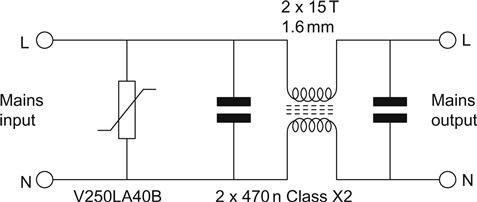
A 130 J metal oxide varistor is connected across the mains to limit mains spikes. Manufacturers’ data sheets for these devices disingenuously show that a 100 V spike riding on the peak of the mains waveform is clipped very effectively but don’t show that a 340 V spike sitting on the 0 V crossing point would pass by unmolested. Still, the day might come when one is needed.
The series common-mode choke is terminated at each end by a pair of Class X2 capacitors. X2 capacitors are the only type of capacitors that may be legally connected between mains line and neutral (the reason is that they are specifically designed to fail safely). Many RFI filters also include a 4.7 nF Class Y capacitor from live to earth, and another from neutral to earth, but their utility is debatable for audio equipment as they can make the earth noisy.
If the HT mains transformer has an electrostatic screen, it should be connected directly to chassis. The heater transformer won’t have an electrostatic screen because it is of split bobbin construction.
We can draw a full power supply circuit diagram (see Figure 5.65).
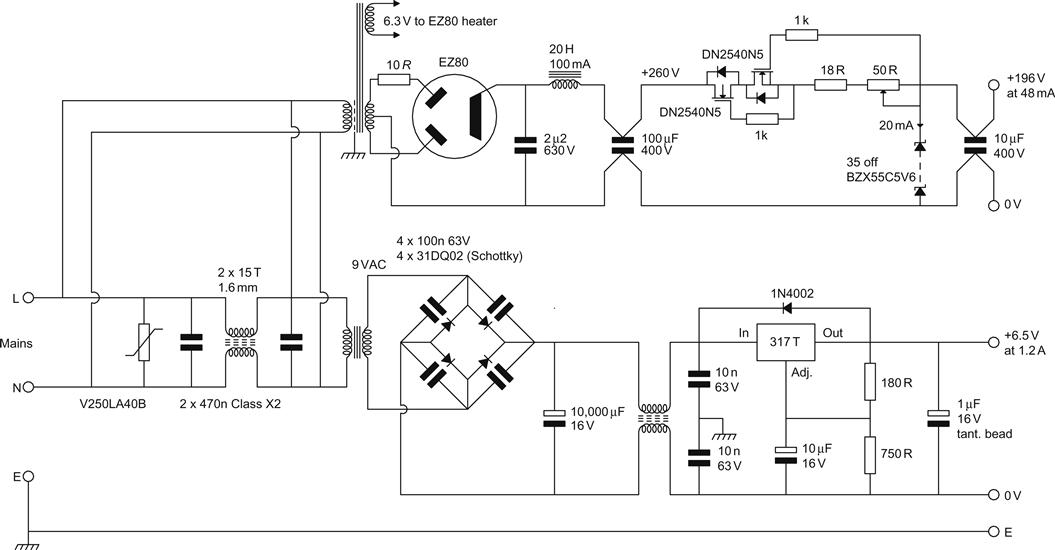
Adapting the Power Supply to the EC8010 RIAA Stage
The balanced hybrid RIAA stage required an HT of 195 V at 46 mA, but the EC8010 RIAA stage requires 390 V at 67 mA, and a pair of references (40 V, 270 V) at zero current. Rather than a single heater supply of 6.3 V at 1.2 A, the EC8010 RIAA stage needs four 300 mA at 12.6 V supplies tied to ≈40 V that can all come from one transformer secondary and a further two 300 mA at 12.6 V supplies tied to ≈270 V requiring another transformer secondary. The heater strings were configured in this way to enable use of a standard transformer having two secondaries of the same voltage. We will need:
HT Regulation
We will again use the statistical regulator because of its low noise. 390 V might seem an alarming voltage to set from 5.6 V Zeners, but it’s simply two 195 V composite Zeners in series (70×5.6 V Zeners). The increased current demand is potentially more of a problem as 67 mA of load current plus 20 mA Zener quiescent current requires 87 mA from the CCS, and if the load should fail, the CCS would sink all 87 mA into the composite Zener. The author was nervous that 87 mA was far too close to the 89 mA maximum rating, so he simulated the inside of an RIAA stage by covering a single Zener with a sheet of cardboard to prevent proper cooling, and then tested it (see Figure 5.66).
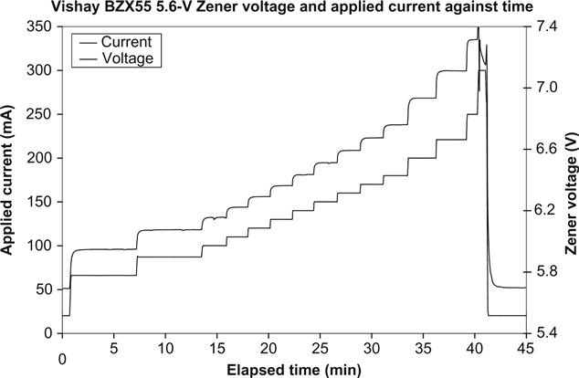
Measurements were logged at 1 s intervals using a pair of Agilent 34410A 6½ digit DMMs. The exponential curve following the transient on the Zener voltage (upper trace) is due to the wires and silicon within the Zener heating and increasing their resistance as a result of the increased applied current (lower trace). The Zener was run for a short time at the statistical regulator’s design current of 20 mA, then increased to 68 mA to simulate a fault in the balanced hybrid RIAA stage, and then 87 mA to simulate a fault in the EC8010 RIAA stage. The Zener survived 5 min at 87 mA, so it was clearly time for some abuse. Current was increased in 10 mA steps and left for roughly 150 s each time. After half an hour of this, the author’s patience was running thin, and he finally applied 300 mA, which did provoke a reaction (smoke from the cardboard and a spike on the graph), so he backed the current off to the original 20 mA. Astonishingly, despite discoloured lead-outs, once the Zener had cooled its voltage at 20 mA was within 0.1% of the original voltage.
There seems to be no justification for fearing damage to the composite Zener from a fault causing its current to rise to 87 mA.
Reference Voltages
The 40 V and 270 V references could be tapped off the statistical regulator’s composite Zener, but having devised an astonishingly low-noise regulator, the author isn’t about to ruin it by injecting mains interference via the inter-winding capacitance of a mains transformer, even if that capacitance would be divided down by a transistor’s hfe.
The safest solution is to use a THINGY configured for 40 V and 270 V and feed it from the raw supply before the regulator so that any mains interference that does manage to crawl back through the THINGY can be attenuated 100 dB by the statistical regulator.
HT Rectification and Smoothing (a PSUD2 Exercise)
We require 390 V, and we need at least 20 V across the statistical regulator’s CCS, so if we allow 10% for mains variation, we need 451 V, say 460 V. This voltage is beyond what a single electrolytic capacitor could tolerate, and putting a pair in series would double typical series inductance from 18 nH to 36 nH, add 20 mm of wire at 0.75 nH/mm, and we would have ≈50 nH, guaranteeing poor RF filtering. Once again it makes sense to use an LC filter using a plastic capacitor having a Kelvin connection. The capacitor needs to be rated at 600 V, so 100 μF would be larger than that can be wound, but 47 μF is feasible.
A valve rectifier allows HT to be applied gently, and the critical parameter governing rectifier choice is now voltage rather than current rating. The traditional choice would have been a GZ34, but these are now far too expensive and a pair of 6CK3/6CL3 damper diodes is far cheaper. If we don’t want to use a centre-tapped transformer, a hybrid bridge rectifier can be made by adding a pair of STTA512Fs to the 6CK3/6CL3.
For an 80 dB signal-to-hum ratio, the EC8010 RIAA stage requires ripple on the 390 V HT to be <1.7 mVpk–pk (slightly less tolerant than the balanced hybrid RIAA stage). The statistical regulator is certain to have >90 dB ripple attenuation, so this corresponds to it tolerating 53 Vpk–pk ripple post-rectification. As before, this means we don’t have to worry greatly about ripple and can concentrate on obtaining the required voltage using available components and ensuring Low Frequency stability.
When you experiment with PSUD2, you will quickly discover that it is difficult to achieve Low Frequency stability in an LC filter having a 47 μF capacitor. The inductance of the choke can be halved from 20 H to 10 H (reducing the L/C ratio) to ease the problem, but Low Frequency stability can only be achieved by adding a capacitor before the choke. Even so, with typical transformer and choke resistances, only a capacitor of around 3–4 μF before the choke completely eliminates Low Frequency ringing. It seems we have designed another intermediate mode supply.
Given that low frequency stability specified the filter components quite tightly, the required 460 VDC output voltage can only be achieved by adjusting the transformer secondary voltage to 400 VRMS (off-load) (see Figure 5.67).
Having achieved the required DC voltage, we find that the ripple is 680 mVpk–pk, so there will be no problem in achieving our 80 dB signal-to-hum ratio.
This is the point where we consider it a mild nuisance that PSUD2 works with off-load voltages because transformers are specified by their on-load voltage. There are two ways around this problem: either use the bar at the bottom of the screen to reveal the on-load RMS voltage leaving the transformer, or make a guess as to typical transformer regulation. Although the first method seems the best, it contains the hidden assumption that you guessed secondary and reflected primary resistance correctly. The author prefers to make the sweeping assumption that 50–100 VA transformers have ≈10% regulation, so that an off-load voltage of 400 VRMS corresponds to an on-load voltage of 372 VRMS. This can be used as a rough check on the accuracy of your initial guess as to transformer secondary and reflected primary resistance – if you have guessed it reasonably well, the PSUD2 voltage will be about 3% lower than the 10% regulation guesstimate. (This discrepancy occurs because PSUD2 can’t model core losses.)
Heater Regulation
The heaters in the EC8010 RIAA stage are run constant current rather than constant voltage and all six strings need 300 mA at an expected maximum voltage of 12.6 V. The 317T can be configured to produce a constant current very easily by placing a single resistor between OUT and ADJ that drops 1.25 V at the chosen current (see Figure 5.68).
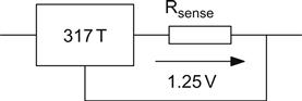
A 4.17 Ω current sense resistor is needed, and this can be achieved by a 4.7 Ω resistor in parallel with 36 Ω. The required power rating (0.33 W) of the 4.7 Ω resistor combined with 1% precision used to be a problem, but TO-220 package 4.7 Ω 1% 20 W resistors are now readily available. Each regulator can be made very simply by fitting the TO-220 resistor adjacent to the 317T on the heatsink and hard-wiring them and the 36 Ω resistor (no PCB needed).
When the heaters are cold, their resistance is low, so almost the entire reservoir capacitor’s voltage appears across each 317T, almost doubling its thermal dissipation, but after 20 s dissipation drops to normal (see Figure 5.69).
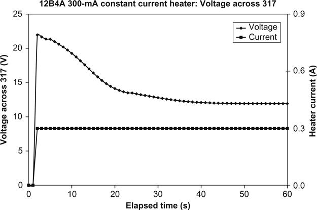
Heater Rectification and Smoothing (a Manual Exercise)
The 317T needs >3 V across it to regulate cleanly and 1.25 V is dropped across the current sense resistor, so we need 4.25 V more than the expected 12.6 V across each heater string, implying 17 V minimum required across the reservoir capacitor.
Looking from the other direction, 2×18 V transformers are common, so they would produce 25.5 Vpk or 22.9 V if the mains drops by 10%. The bridge rectifier will drop 1.4 V, leaving 21.5 V, allowing 4.5 V of ripple. Each series chain requires 300 mA, so the four chains require a total of 1.2 A, and the other two chains require a total 600 mA. The 1.2 A supply requires a 3,300 μF capacitor for 3.6 Vpk–pk ripple, whereas 1,500 μF would suffice for 600 mA supply. Although it might be easier to use 3,300 μF for both, it would halve the ripple voltage on the 600 mA supply, raising the DC voltage and unnecessarily increasing the dissipation of the associated 317T.
The total DC current is 1.8 A from our raw 25.5 Vpk, so this is 46 W, requiring a 50 VA transformer having a split bobbin or foil electrostatic screen to minimise common-mode interference.
Now that we know the voltage on the reservoir capacitor, we can estimate the thermal dissipation of each 317T. If we treat the DC on the reservoir as being its peak voltage minus half the ripple, then:
Each heater chain drops 12.6 V, and 1.25 V is dropped across the current sense resistor, leaving 9.85 V across the 317T, and P=IV=9.85 V×0.3 A≈3 W. It is convenient to mount all six 317Ts on a common heatsink (via insulating kits), so it must dissipate 18 W, and for a 20 °C temperature rise, that implies a thermal resistance of <1.1 °C/W.
We now have a full power supply circuit diagram (see Figure 5.70).