
CHAPTER 1
Signal Integrity Is in Your Future
“There are two kinds of engineers: Those who have signal-integrity problems and those who will.”
—Eric Bogatin
Ironically, this is an era when not only are clock frequencies increasing and signal-integrity problems getting more severe, but the time design teams are available to solve these problems and designed new products are getting shorter. Product design teams have one chance to get a product to the market; the product must work successfully the first time. If identifying and eliminating signal-integrity problems isn’t an active priority early in the product design cycle, chances are the product will not work.
TIP
As clock frequencies and data rates increase, identifying and solving signal-integrity problems becomes critical. The successful companies will be those that master signal-integrity problems and implement an efficient design process to eliminate these problems. It is by incorporating best design practices, new technologies, and new analysis techniques and tools that higher-performance designs can be implemented and meet ever-shrinking schedules.
In high-speed products, the physical and mechanical design can affect signal integrity. Figure 1-1 shows an example of how a simple 2-inch-long section of trace on a printed circuit board (PCB) can affect the signal integrity from a typical driver.

Figure 1-1 100-MHz clock waveform from a driver chip when there is no connection (smooth plot) and when there is a 2-inch length of PCB trace connected to the output (ringing). Scale is 1 v/div and 2 nsec/div, simulated with Mentor Graphics HyperLynx.
The design process is often a very intuitive and creative process. Feeding your engineering intuition about signal integrity is critically important to reaching an acceptable design as quickly as possible.
All engineers who touch a product should have an understanding of how what they do may influence the performance of the overall product. By understanding the essential principles of signal integrity at an intuitive and engineering level, every engineer involved in the design process can evaluate the impact of his or her decisions on system performance. This book is about the essential principles needed to understand signal-integrity problems and their solutions. The engineering discipline required to deal with these problems is presented at an intuitive level and a quantitative level.
1.1 What Are Signal Integrity, Power Integrity, and Electromagnetic Compatibility?
In the good old days of 10-MHz clock frequencies, the chief design challenges in circuit boards or packages were how to route all the signals in a two-layer board and how to get packages that wouldn’t crack during assembly. The electrical properties of the interconnects were not important because they didn’t affect system performance. In this sense, we say that the interconnects were “transparent to the signals.”
A device would output a signal with a rise time of roughly 10 nsec and a clock frequency of 10 MHz, for example, and the circuits would work with the crudest of interconnects. Prototypes fabricated with wire-wrapped boards worked as well as final products with printed circuit boards and engineering change wires.
But clock frequencies have increased and rise times of signals have decreased. For most electronic products, signal-integrity effects begin to be important at clock frequencies above about 100 MHz or rise times shorter than about 1 nsec. This is sometimes called the high-frequency or high-speed regime. These terms refer to products and systems where the interconnects are no longer transparent to the signals and, if you are not careful, one or more signal-integrity problems arise.
Signal integrity refers, in its broadest sense, to all the problems that arise in high-speed products due to the interconnects. It is about how the electrical properties of the interconnects, interacting with the digital signal’s voltage and current waveforms, can affect performance.
All of these problems fall into one of the following three categories, each with considerable overlap with the others:
1. Signal integrity (SI), involving the distortion of signals
2. Power integrity (PI), involving the noise on the interconnects and any associated components delivering power to the active devices
3. Electromagnetic compatibility (EMC), the contribution to radiated emissions or susceptibility to electromagnetic interference from fields external to the product
In the design process, all three of these electrical performance issues need to be considered for a successful product.
The general area of EMC really encompasses solutions to two problems: too much radiated emission from a product into the outside world and too much interference on a product from radiation coming from the outside world. EMC is about engineering solutions for the product so it will at the same time maintain radiated emissions below the acceptable limit and not be susceptible to radiation from the external world.
When we discuss the solutions, we refer to EMC. When we discuss the problems, we refer to electromagnetic interference (EMI). Usually EMC is about passing a test for radiated emissions and another test for being robust against radiated susceptibility. This is an important perspective as some of the EMC solutions are introduced just to pass certification tests.
TIP
Generally, products can pass all their performance tests and meet all functional specs but still fail an EMC compliance test.
Designing for acceptable EMC involves good SI and PI design as well as additional considerations, especially related to cables, connectors, and enclosure design. Spread spectrum clocking (SSC), which purposely adds jitter to clocks by modulating their clock frequency, is specifically used to pass an EMC certification test.
PI is about the problems associated with the power distribution network (PDN), which includes all the interconnects from the voltage regulator modules (VRMs) to the voltage rail distributed on the die. This includes the power and ground planes in the board and in the packages, the vias in the board to the packages, the connections to the die pads, and any passive components like capacitors connected to the PDN.
While the PDN that feeds the on-die core power rail, sometimes referred to as the Vdd rail, is exclusively a PI issue, there are many overlapping problems between PI and SI topics. This is primarily because the return paths for the signals use the same interconnects usually associated with the PDN interconnects, and anything that affects these structures has an impact on both signal quality and power quality.
TIP
The overlap between PI and SI problems adds confusion to the industry because problems in this gray area are either owned by two different engineers or fall through the cracks as the PI engineer and the SI engineer each think it’s the other’s responsibility.
In the SI domain, problems generally relate to either noise issues or timing issues, each of which can cause false triggering or bit errors at the receiver.
Timing is a complicated field of study. In one cycle of a clock, a certain number of operations must happen. This short amount of time must be divided up and allocated, in a budget, to all the various operations. For example, some time is allocated for gate switching, for propagating the signal to the output gate, for waiting for the clock to get to the next gate, and for waiting for the gate to read the data at the input. Though the interconnects affect the timing budget, timing is not explicitly covered in this book. The influence on jitter from rise-time distortion, created from the interconnects, is extensively covered.
For the details on creating and managing timing budgets, we refer any interested readers to a number of other books listed Appendix C, “Selected References,” for more information on this topic. This book concentrates on the effects of the interconnects on the other generic high-speed problem: too much noise.
We hear about a lot of signal-integrity noise problems, such as ringing, ground bounce, reflections, near-end cross talk, switching noise, non-monotonicity, power bounce, attenuation, and capacitive loading. All of these relate to the electrical properties of the interconnects and how the electrical properties affect the distortion of the digital signals.
It seems at first glance that there is an unlimited supply of new effects we have to take into account. This confusion is illustrated in Figure 1-2. Few digital-system designers or board designers are familiar with all of these terms as other than labels for the craters left in a previous product-design minefield. How are we to make sense of all these electrical problems? Do we just keep a growing checklist and add to it periodically?

Figure 1-2 The list of signal-integrity effects seems like a random collection of terms, without any pattern.
Each of the effects listed above, is related to one of the following six unique families of problems in the fields of SI/PI/EMC:
1. Signal distortion on one net
2. Rise-time degradation from frequency-dependent losses in the interconnects
3. Cross talk between two or more nets
4. Ground and power bounce as a special case of cross talk
5. Rail collapse in the power and ground distribution
6. Electromagnetic interference and radiation from the entire system
These six families are illustrated in Figure 1-3. Once we identify the root cause of the noise associated with each of these six families of problems, and understand the essential principles behind them, the general solution for finding and fixing the problems in each family will become obvious. This is the power of being able to classify every SI/PI/EMC problem into one of these six families.

These problems play a role in all interconnects, from the smallest on-chip wire to the cables connecting racks of boards and everywhere in-between. The essential principles and effects are the same. The only differences in each physical structure are the specific geometrical feature sizes and the material properties.
1.2 Signal-Integrity Effects on One Net
A net is made up of all the metal connected together in a system. For example, there may be a trace going from a clock chip’s output pin to three other chips. Each piece of metal that connects all four of these pins is considered one net. In addition, the net includes not only the signal path but also the return path for the signal current.
There are three generic problems associated with signals on a single net being distorted by the interconnect. The first is from reflections. The only thing that causes a reflection is a change in the instantaneous impedance the signal encounters. The instantaneous impedance the signal sees depends as much on the physical features of the signal trace as on the return path. An example of two different nets on a circuit board is shown in Figure 1-4.

Figure 1-4 Example of two nets on a circuit board. All metal connected together is considered one net. Note: One net has a surface-mount resistor in series. Routed with Mentor Graphics HyperLynx.
When the signal leaves the output driver, the voltage and the current, which make up the signal, see the interconnect as an electrical impedance. As the signal propagates down the net, it is constantly probing and asking, “What is the instantaneous impedance I see?” If the impedance the signal sees stays the same, the signal continues undistorted. If, however, the impedance changes, the signal will reflect from the change and continue through the rest of the interconnect distorted. The reflection itself will reflect off other discontinuities and will rattle around the interconnect, some of it making its way to the receiver, adding distortions. If there are enough impedance changes, the distortions can cause false triggering.
Any feature that changes the cross section or geometric shape of the net will change the impedance the signal sees. We call any feature that changes the impedance a discontinuity. Every discontinuity will, to some extent, cause the signal to be distorted from its original pristine shape. For example, some of the features that would change the impedance the signal sees include the following:
• An end of the interconnect
• A line-width change
• A layer change through a via
• A gap in return-path plane
• A connector
• A routing topology change, such as a branch, tee, or stub
These impedance discontinuities can arise from changes in the cross section, the topology of the routed traces, or the added components. The most common discontinuity is what happens at the end of a trace, which is usually either a high impedance open at the receiver or a low impedance at the output driver.
If the source of reflection noise is changes in the instantaneous impedance, then the way to fix this problem is to engineer the impedance of the interconnect to be constant.
TIP
The way to minimize the problems associated with impedance changes is to keep the instantaneous impedance the signal sees constant throughout the net.
This strategy is typically implemented by following four best design practices:
1. Use a board with constant, or “controlled,” impedance traces. This usually means using uniform transmission lines.
2. To manage the reflections from the ends, use a termination strategy that controls the reflections by using a resistor to fool the signal into not seeing an impedance change.
3. Use routing rules that allow the topology to maintain a constant impedance down the trace. This generally means using point-to-point routing or minimum-length branch or short stub lengths.
4. Engineer the structures that are not uniform transmission lines to reduce their discontinuity. This means adjusting fine geometrical design features to sculpt the fringe fields.
Figure 1-5 shows an example of poor signal quality due to impedance changes in the same net and when a terminating resistor is used to manage the impedance changes. Often, what we think of as “ringing” is really due to reflections associated with impedance changes.

Figure 1-5 Ringing in an unterminated line and good signal quality in a source-series terminated interconnect line. The PCB trace is only 2 inches long in each case. Scale is 1 v/div and 2 nsec/div. Simulated with Mentor Graphics HyperLynx.
Even with perfect terminations, the precise board layout can drastically affect signal quality. When a trace branches into two paths, the impedance at the junction changes, and some signal will reflect back to the source, while some will continue down the branches in a reduced and distorted form. Rerouting the trace to be a daisy chain causes the signal to see a constant impedance all down the path, and the signal quality can be restored.
The impact on a signal from any discontinuity depends on the rise time of the signal, where the discontinuity is in the circuit and other sources of reflections are in the circuit. As the rise time gets shorter, the magnitude of the distortion on the signal will increase. This means that a discontinuity that was not a problem in a 33-MHz design with a 3-nsec rise time may be a problem in a 100-MHz design with a 1-nsec rise time. This is illustrated in Figure 1-6.
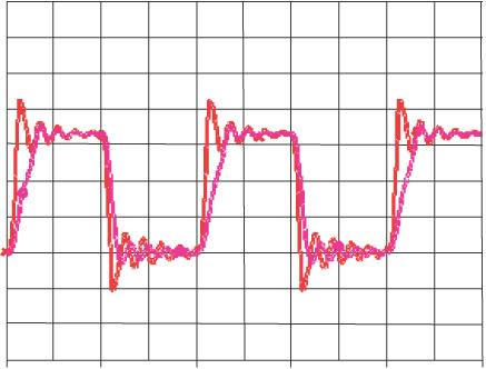
Figure 1-6 25-MHz clock waveforms with a PCB trace 6 inches long and unterminated. The slow rise time is a 3-nsec rise time. The ringing is from a rise time of 1 nsec. What may not have been a problem with one rise time can be a problem with a shorter rise time. Scale is 1 v/div and 5 nsec/div. Simulated with Mentor Graphics HyperLynx.
The higher the frequency and the shorter the rise time, the more important it is to keep the impedance the signal sees constant. One way of achieving this is by using controlled impedance interconnects even in the packages, such as with multilayer ball grid arrays (BGAs). When the packages do not use controlled impedance, such as with lead frames, it’s important to keep the leads short, such as by using chip-scale packages (CSPs).
There are two other aspects of signal integrity associated with one net. Frequency-dependent losses in the line from the conductor and the dielectric cause higher-frequency signal components to be attenuated more than the lower-frequency components. The end result is an increase in the rise time of the signal as it propagates. When this rise-time degradation approaches the unit interval of a single bit, information from one bit will leak into the next bit and the next bit. This effect is called intersymbol interference (ISI) and is a significant source of problems in high-speed serial links, in the 1 gigabit per second (Gbps) and higher regime.
The third aspect of signal-quality problems associated with a single net is related to timing. The time delay difference between two or more signal paths is called skew. When a signal and clock line have a skew different than expected, false triggering and errors can result. When the skew is between the two lines that make up a differential pair, some of the differential signal will be converted into common signal, and the differential signal will be distorted. This is a special case of mode conversion, and it will result in ISI and false triggering.
While skew is a timing problem, it often arises due to the electrical properties of the interconnect. The first-order impact on skew is from the total length of the interconnects. This is easily controlled with careful layout to match lengths. However, the time delay is also related to the local dielectric constant that each signal sees and is often a much more difficult problem to fix.
TIP
Skew is the time delay difference between two or more nets. It can be controlled to first order by matching the length of the nets. In addition, the local variation in dielectric constant between the nets, as from the glass weave distribution in the laminate, will also affect the time delay and is more difficult to control.
1.3 Cross Talk
When one net carries a signal, some of this voltage and current can pass over to an adjacent quiet net, which is just sitting there, minding its own business. Even though the signal quality on the first net (the active net) is perfect, some of the signal can couple over and appear as unwanted noise on the second, quiet net.
TIP
It is the capacitive and inductive coupling between two nets that provides a path for unwanted noise from one net to the other. It can also be described in terms of the fringe electric and magnetic fields from an aggressor to a victim line.
Cross talk occurs in two different environments: when the interconnects are uniform transmission lines, as in most traces in a circuit board, and when they are not uniform transmission lines, as in connectors and packages. In controlled-impedance transmission lines where the traces have a wide uniform return path, the relative amount of capacitive coupling and inductive coupling is comparable. In this case, these two effects combine in different ways at the near end of the quiet line and at the far end of the quiet line. An example of the measured near- and far-end cross talk between two nets in a circuit board is shown in Figure 1-7.
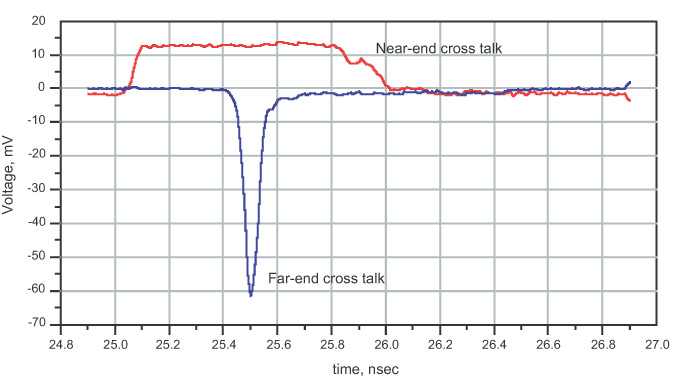
Figure 1-7 Measured voltage noise at the near end and the far end of a quiet trace when a 200-mV signal is injected in the active trace. Note the near-end noise is about 7% and the far-end noise is nearly 30% of the signal. Measurements performed with an Agilent DCA86100 with time-domain reflectometer (TDR) plug-in.
Having a wide uniform plane as the return path is the configuration of lowest cross talk. Anything that changes the return path from a wide uniform plane will increase the amount of coupled noise between two transmission lines. Usually when this happens—for example, when the signal goes through a connector and the return paths for more than one signal path are now shared by one of the pins rather than by a plane—the inductively coupled noise increases much more than the capacitively coupled noise.
In this regime, where inductively coupled noise dominates, we usually refer to the cross talk as switching noise, delta I noise, dI-dt noise, ground bounce, simultaneous switching noise (SSN), or simultaneous switching output (SSO) noise. As we will see, this type of noise is generated by the coupling inductance, which is called mutual inductance. Switching noise occurs mostly in connectors, packages, and vias, where the return path conductor is not a wide, uniform plane.
Ground bounce, reviewed later in this book, is really a special case of cross talk caused when return currents overlap in the same conductor and their mutual inductance is very high. Figure 1-8 shows an example of SSO noise from the high mutual inductance between adjacent signal and return paths in a package.

Figure 1-8 Top trace: Measured voltage on active lines in a multiline bus. Bottom trace: Measured noise on one quiet line showing the switching noise due to mutual inductance between the active and quiet nets in the package.
TIP
SSO noise, where the coupled or mutual-inductance dominates is the most important issue in connector and package design. It will only get worse in next-generation products. The solution lies in careful design of the geometry of paths so that mutual inductance is minimized and in the use of differential signaling.
By understanding the nature of capacitive and inductive coupling, described as either lumped elements or as fringe electric and magnetic fields, it is possible to optimize the physical design of the adjacent signal traces to minimize their coupling. This usually can be as simple as spacing the traces farther apart. In addition, the use of lower-dielectric constant material will decrease the cross talk for the same characteristic impedance lines. Some aspects of cross talk, especially switching noise, increase with the length of the interconnect and with decreasing rise time. Shorter rise-time signals will create more cross talk. Keeping interconnects short, such as by using CSPs and high-density interconnects (HDIs), helps minimize cross talk.
1.4 Rail-Collapse Noise
Noise is generated, and is a problem, in more than just the signal paths. It can also be a disaster in the power- and ground-distribution network that feeds each chip. When current through the power- and ground-path changes, as when a chip switches its outputs or core gates switch, there will be a voltage drop across the impedance of the power and ground paths. When there are reactive elements in the PDN, especially with parallel resonances, switching power currents can also result in higher voltage spikes on the power rail.
This voltage noise means a lower or higher voltage on the rail pads of the chip. A change in the voltage on the power rails can result in either voltage noise on signal lines, which can contribute to false triggering and bit errors or to enhanced jitter. Figure 1-9 shows one example of the change in the voltage across a microprocessor’s power rails.

Figure 1-9 Measured Vcc voltage at three pin locations on the package of a microprocessor just coming from a “stop-clock” state. Nominal voltage is supposed to be 2.5 V, but due to voltage drops in the power distribution system, the delivered voltage collapses by almost 125 mV.
PDN noise can also cause jitter. The propagation delay for the turn-on of a gate is related to the voltage between the drain and source. When the voltage noise increases the rail voltage, gates switch faster, and clock and data edges are pulled in. When the voltage noise brings the rail voltage lower, gates switch more slowly, and clock and data edges are pushed out. This impact on the edge of clocks and signals is a dominant source of jitter.
In high-performance processors, FPGAs, and some ASICs, the trend is for lower power-supply voltage but higher power consumption. This is primarily due to more gates on a chip switching faster. In each cycle, a certain amount of energy is consumed. When the chip switches faster, the same energy is consumed in each cycle, but it is consumed more often, leading to higher power consumption.
These factors combined mean that higher currents will be switching in shorter amounts of time, and with lower signal voltage swings, the amount of noise that can be tolerated will decrease. As the drive voltage decreases and the current level increases, any voltage drops associated with rail collapse become bigger and bigger problems.
As these power rail currents travel through the impedance of the PDN interconnects, they generate a voltage drop across each element. This voltage drop is the source of power rail noise.
To reduce the voltage noise on the power rails when power supply currents switch, the most important best design practice is to engineer the PDN as a low impedance.
In this way, even though there is current switching in the PDN, the voltage drop across a lower impedance may be kept to an acceptable level. Sun Microsystems has evaluated the requirements for the impedance of the PDN for high-end processors. Figure 1-10 shows Sun’s estimate of the required impedance of the PDN. Lower impedance in the PDN is increasingly important and harder to achieve.

Figure 1-10 Trend in the maximum allowable impedance of the power distribution system for high-end processors. Source: Sun Microsystems.
If we understand how the physical design of the interconnects affects their impedance, we can optimize the design of the PDN for low impedance. As we will see, designing a low-impedance PDN means including features such as:
1. Closely spaced adjacent planes for the power and ground distribution with as thin a dielectric between them as possible, near the surface of the board
2. Multiple, low-inductance decoupling capacitors
3. Multiple, very short power and ground leads in packages
4. A low-impedance VRM
5. On-package decoupling (OPD) capacitors
6. On-chip decoupling (ODC) capacitors
An innovative technology to help minimize rail collapse can be seen in the new ultrathin, high-dielectric constant laminates for use between power and ground layers. One example is C-Ply from 3M Corp. This material is 8 microns thick and has a dielectric constant of 20. Used as the power and ground layers in an otherwise conventional board, the ultralow loop inductance and high distributed capacitance dramatically reduce the impedance of the power and ground distribution. Figure 1-11 shows an example of the rail-collapse noise on a small test board using conventional layers and a board with this new C-Ply.

Figure 1-11 Measured rail voltage noise on a small digital board, with various methods of decoupling. The worst case is no decoupling capacitors on FR4. The best case is the 3M C-Ply material, showing virtually no voltage noise. Courtesy of National Center for Manufacturing Science. Scale is 0.5 v/div and 5 nsec/div.
1.5 Electromagnetic Interference (EMI)
With board-level clock frequencies in the 100-MHz to 500-MHz range, the first few harmonics are within the common communications bands of TV, FM radio, cell phone, and personal communications services (PCS). This means there is a very real possibility of electronic products interfering with communications unless their electromagnetic emissions are kept below acceptable levels. Unfortunately, without special design considerations, EMI will get worse at higher frequencies. The radiated far-field strength from common currents will increase linearly with frequency and from differential currents will increase with the square of the frequency. With clock frequencies increasing, the radiated emissions level will inevitably increase as well.
It takes three things to have an EMI problem: a source of noise, a pathway to a radiator, and an antenna that radiates. Every source of signal-integrity problem mentioned above will be a source of EMI. What makes EMI so challenging is that even if the noise is low enough to meet the signal-integrity and power-integrity noise budget, it may still be large enough to cause serious radiated emissions.
TIP
The two most common sources of EMI are (1) the conversion of some differential signal into a common signal, which eventually gets out on an external twisted-pair cable, and (2) ground bounce on a circuit board generating common currents on external single-ended shielded cables. Additional noise can come from internally generated radiation leaking out of the enclosure.
Most of the voltage sources that drive radiated emissions come from the power- and ground-distribution networks. Often, the same physical design features that contribute to low rail-collapse noise will also contribute to lower emissions.
Even with a voltage noise source that can drive radiation, it is possible to isolate it by grouping the high-speed sections of a board away from where they might exit the product. Shielding the box will minimize the leakage of the noise from an antenna. Many of the ills of a poorly designed board can be fixed with a good shield.
A product with a great shield will still need to have cables connecting it to the outside world for communications, for peripherals, or for interfacing. Typically, the cables extending outside the shielded enclosure act as the antennas, and radiate. The correct use of ferrites on all connected cables, especially on twisted pair, will dramatically decrease the efficiency of the cables as antennas. Figure 1-12 shows a close-up of the ferrite around a cable.

Figure 1-12 Ferrite choke around a cable, split apart. Ferrites are commonly used around cables to decrease common currents, a major source of radiated emissions. Courtesy of IM Intermark.
The impedance associated with the I/O connectors, especially the impedance of the return-path connections, will dramatically affect the noise voltages that can drive radiating currents. The use of shielded cables with low-impedance connections between the shields and chassis will go a long way to minimize EMI problems.
Unfortunately, for the same physical system, increasing the clock frequency generally will also increase the radiated emissions level. This means that EMI problems will be harder to solve as clock frequencies increase.
1.6 Two Important Signal-Integrity Generalizations
Two important generalizations should be clear from looking at the six signal-integrity problems above.
First, each of the six families of problems gets worse as rise times decrease. All the signal-integrity problems above scale with how fast the current changes or with how fast the voltage changes. This is often referred to as dI/dt or dV/dt. Shorter rise times mean higher dI/dt and dV/dt.
It is unavoidable that as rise times decrease, the noise problems will increase and be more difficult to solve. And, as a consequence of the general trends in the industry, the rise times found in all electronic products will continually decrease. This means that what might not have caused a problem in one design may be a killer problem in the next design with the next-generation chip sets operating with a shorter rise time. This is why it is often said that “there are two kinds of engineers: Those who have signal-integrity problems and those who will.”
The second important generalization is that effective solutions to signal-integrity problems are based heavily on understanding the impedance of interconnects. If we have a clear intuitive sense of impedance and can relate the physical design of the interconnects with their impedance, many signal-integrity problems can be eliminated during the design process.
This is why an entire chapter in this book is devoted to understanding impedance from an intuitive and engineering perspective and why much of the rest of this book is about how the physical design of interconnects affects the impedance seen by signals and power and ground currents.
1.7 Trends in Electronic Products
Our insatiable thirst for ever higher performance at ever higher densities and at lower cost drives the electronics industry. This is both in the consumption of information as in video images and games, and in the processing and storage of information in industries like bioinformatics and weather or climate forecasting.
In 2015, almost 50% of Internet traffic was in the form of video images from Netflix and YouTube. The data rate of information flowing on the Internet backbone doubles almost every year.
A few trips to the local computer store over the past 10 years will have given anyone a good sense of the incredible treadmill of progress in computer performance. One measure of performance is the clock frequency of a processor chip. The trend for Intel processor chips, as illustrated in Figure 1-13, shows a doubling in clock frequency about every two years.

Figure 1-13 Historical trend in the clock frequency of Intel processors based on year of introduction. The trend is a doubling in clock frequency every two years. Source: Intel Corp.
In some processor families, the clock frequencies have saturated, but the data rates for signals communicating chip to chip and board to board have continued to increase at a steady rate.
This trend toward ever-higher clock frequency and data rates is enabled by the same force that fuels the semiconductor revolution: photolithography. As the gate channel length of transistors is able to be manufactured at smaller size, the switching speed of the transistor increases. The electrons and holes have a shorter distance to travel and can transit the gate, effecting transitions, in a shorter time when the channel length is shorter.
When we refer to a technology generation as 0.18 microns or 0.13 microns, we are really referring to the smallest channel length that can be manufactured. The shorter switching time for smaller channel-length transistors has two important consequences for signal integrity.
The minimum time required for one clock cycle is limited by all the operations that need to be performed in one cycle. Usually, there are three main factors that contribute to this minimum time: the intrinsic time for all the gates that need to switch in series, the time for the signals to propagate through the system to all the gates that need to switch, and the setup and hold times needed for the signals at the inputs to be read by the gates.
In single-chip microprocessor-based systems, such as in personal computers, the dominant factor influencing the minimum cycle time is the switching speed of the transistors. If the switching time can be reduced, the minimum total time required for one cycle can be reduced. This is the primary reason clock frequencies have increased as feature size has been reduced.
TIP
It is inevitable that as transistor feature size continues to reduce, rise times will continue to decrease, and clock frequencies and data rates will continue to increase.
Figure 1-14 shows projections from the 2001 Semiconductor Industry Association (SIA) International Technology Roadmap for Semiconductors (ITRS) for future on-chip clock frequencies, based on projected feature size reductions, compared with the Intel processor trend. This shows the projected trend for clock frequency increasing at a slightly diminishing but still growing rate for the next 15 years as well. In the recent past and going forward, while clock frequencies have saturated at about 3 GHz, the communications data rates are on a steady, exponential growth rate and will exceed 56 Gbps per channel by 2020.
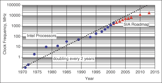
Figure 1-14 Historical trend in the clock frequency of Intel processors based on year of introduction. The trend is a doubling in clock frequency every two years. Also included is the Semiconductor Industry Association roadmap expectations. Source: Intel Corp. and SIA.
As the clock frequency increases, the rise time of the signals must also decrease. Each gate that reads either the data lines or the clock lines needs enough time with the signal being either in the high state or the low state, to read it correctly.
This means only a short time is left for the signal to be in transition. We usually measure the transition time, either the rise time or the fall time, as the time it takes to go from 10% of the final state to 90% of the final state. This is called the 10–90 rise time. Some definitions use the 20% to 80% transition points and this rise time is referred to as the 20–80 rise time. Figure 1-15 shows an example of a typical clock waveform and the time allocated for the transition. In most high-speed digital systems, the time allocated to the rise time is about 10% of the clock cycle time, or the clock period.

Figure 1-15 The 10–90 rise time for a typical clock waveform is roughly 10% of the period. Scale is 1 v/div and 2 nsec/div, simulated with Mentor Graphics HyperLynx.
This is a simple rule of thumb, not a fundamental condition. In legacy systems with a high-end ASIC or FPGA but older peripherals, the rise time might be 1% of the clock period. In a high-speed serial link, pushing the limits to the highest data rate possible, the rise time may be 50% of the unit interval.
Based on this rule of thumb, the rise time is roughly related to the clock frequency by:
where:
RT = rise time, in nsec
Fclock = clock frequency, in GHz
For example, when the clock frequency is 1 GHz, the rise time of the associated signals is about 0.1 nsec, or 100 psec. When the clock frequency is 100 MHz, the rise time is roughly 1 nsec. This relationship is shown in Figure 1-16.

Figure 1-16 Rise time decreases as the clock frequency increases. Signal-integrity problems usually arise at rise times less than 1 nsec or at clock frequencies greater than 100 MHz.
TIP
The treadmill-like advance of ever-increasing clock frequency means an ever-decreasing rise time and signal-integrity problems that are harder to solve.
Of course, this simple relationship between the rise time of a signal and the clock frequency is only a rough approximation and depends on the specifics of the system. The value in such simple rules of thumb is being able to get to an answer faster, without knowing all the necessary information for an accurate answer. It is based on the very important engineering principle “Sometimes an OKAY answer NOW! is more important than a good answer LATE.” Always be aware of the underlying assumptions in rules of thumb.
Even if the clock frequency of a product is low, there is still the danger of shorter rise times as a direct consequence of the chip technology. A chip-fabrication factory, usually called a “fab,” will try to standardize all its wafers on one process to increase the overall yield. The smaller the chip size, the more chips can be fit on a wafer and the lower the cost per chip. Even if the chip is going to be used in a slow-speed product, it may be fabricated on the same line as a leading-edge ASIC, with the same small-feature size.
Ironically, the lowest-cost chips will always have ever-shorter rise times, even if they don’t need it for the specific application. This is an unintended, scary consequence of Moore’s Law. If you have designed a chip set into your product and the rise time is 2 nsec, for example, with a 50-MHz clock, there may be no signal-integrity problems. When your chip supplier upgrades its fab line with a finer-feature process, it may provide you with lower-cost chips. You may think you are getting a good deal. However, these lower-cost chips may now have a rise time of 1 nsec. This shorter rise time may cause reflection noise, excess cross talk, and rail collapse, and the chips may fail the Federal Communications Commission (FCC) EMC certification tests. The clock frequency of your product hasn’t changed, but, unknown to you, the rise time of the chips supplied to you has decreased with the newer, finer-feature manufacturing process.
TIP
As all fabs migrate to lower-cost, finer-feature processes, all fabricated chips will have shorter rise times, and signal-integrity problems have the potential to arise in all products, even those with clock frequencies below 50 MHz.
It’s not just microprocessor-based digital products that are increasing in clock frequency and decreasing in rise times. The data rate and clock frequencies used in high-speed communications are blowing past the clock frequencies of microprocessor digital products.
One of the most common specifications for defining the speed of a high-speed serial link is the optical carrier (OC) spec. This is actually a data rate, with OC-1 corresponding to about 50 megabits per second (Mbps). OC-48, with a data rate of 2.5 gigabits per second (Gbps), is in high-volume deployment and widely implemented. OC-192, at 10 Gbps, is just ramping up. In the near future, OC-768, at 40 Gbps, will be in wide-scale deployment.
The OC designation is a specification for data rate, not for clock frequency. Depending on how a bit is encoded in the data stream, the actual clock frequency of a system can be higher or lower than the data rate.
For example, if there is one bit per clock cycle, then the actual clock frequency will be the data rate. If two data bits are encoded per clock cycle, the underlying clock frequency will be half the data rate. A 2.5-Gbps data rate can be obtained with a 1.25-GHz clock. The more bits in the data stream used for routing information or error correction and overhead, the lower the data rate, even though the clock frequency is constant.
Commonly used signaling protocols like PCIe, SATA, and Gigabit Ethernet all use a non-return-to-zero (NRZ) signaling scheme, which encodes two bits in each clock cycle. This means that the underlying clock, apparent with the highest transition density signal, such as 1010101010, will have a clock frequency half the data rate. We refer to this underlying clock frequency as the Nyquist frequency.
To keep signal-integrity problems at a minimum, the lowest clock frequency and longest rise time should be used. This has inspired a growing trend in data rates in excess of 28 Gbps, to encode four to eight data bits per clock cycle, using multilevel signaling and multiple signal lines in parallel. This technique of encoding bits in the amplitude is called pulse amplitude modulation (PAM).
NRZ, which encodes two bits per cycle, is considered a PAM2 signaling scheme. Using four voltage levels in one unit interval is referred to as PAM4 and is a popular technique for 56-Gbps signaling.
The trend is definitely toward higher data rates. A data rate of 10 Gbps, common for Ethernet systems, has a Nyquist clock frequency of 5 GHz. The unit interval of a 10 Gbps signal is only 100 psec. This means that the rise time must be less than 50 psec. This is a short rise time and requires extremely careful design practices.
High-speed serial links are also used for chip-to-chip and board-to-board communications in all products from cell phones and computers to large servers and mainframes. Whatever bit rate they may start at, they also have a migration path mapped to at least three generations, each one doubling in bit rate. Among these are the following:
• PCI Express, starting at 2.5 Gbps and moving to 5 Gbps, 8 Gbps, and 16 Gbps.
• InfiniBand, starting at 2.5 Gbps and moving to 5 Gbps and 10 Gbps
• Serial ATA (SATA), starting at 1.25 Gbps and moving to 2.5 Gbps, 6 Gbps, and 12 Gbps
• XAUI, starting at 3.125 Gbps and moving to 6.25 Gbps and 10 Gbps
• Gigabit Ethernet, starting at 1 Gbps and moving to 10 Gbps, 25 Gbps, 40 Gbps, and even 100 Gbps.
1.8 The Need for a New Design Methodology
We’ve painted a scary picture of the future. The situation analysis is as follows:
• Signal-integrity problems can prevent the correct operation of a high-speed digital product.
• These problems are a direct consequence of shorter rise time and higher clock frequencies.
• Rise times will continue their inevitable march toward shorter values, and clock frequencies will continue to increase.
• Even if we limit the clock frequency, using the lowest-cost chips means even low-speed systems will have chips with very short rise times.
• We have less time in the product-design cycle to get the product to market; it must work the first time.
What are we to do? How are we to efficiently design high-speed products in this new era? In the good old days of 10-MHz clock systems, when the interconnects were transparent, we did not have to worry about signal-integrity effects. We could get away with designing a product for functionality and ignore signal integrity. In today’s products, ignoring signal integrity invites schedule slips, higher development costs, and the possibility of never being able to ship a functional product.
It will always be more profitable to pay extra to design a product right the first time than to try to fix it later. In the product life cycle, often the first six months in the market are the most profitable. If your product is late, a significant share of the life-cycle profits may be lost. Time really is money.
TIP
A new product-design methodology is required which ensures that signal-integrity problems are identified and eliminated from a product as early in the design cycle as possible. To meet ever-shorter design cycle times, the product must meet performance specifications the first time.
1.9 A New Product Design Methodology
There are six key ingredients to the new product design methodology:
1. Identify which of the specific SI/PI/EMC problems will arise in your product and should be avoided, based on the six families of problems.
2. Find the root cause of each problem.
3. Apply the Youngman Principle to turn the root cause of the problem into best design practices.
4. When it is free and does not add any cost, always follow the best design practices, which we sometimes call habits.
5. Optimize the design for performance, cost, risk, and schedule, by evaluating design trade-offs using analysis tools: rules of thumb, approximations, and numerical simulations (as virtual prototypes.)
6. Use measurements throughout the design cycle to reduce risk and increase confidence of the quality of the predictions.
The basis of this strategy applies not just to engineering SI/PI/EMC problems out of the product but also solving all engineering design problems. The most efficient way of solving a problem is by first finding the root cause. If you have the wrong root cause for the problem, your chance of fixing the problem is based on pure luck.
TIP
Any design or debug process must have as an emphasis finding and verifying the correct root cause of the problem.
The root cause is turned into a best design practice using the Youngman Principle, named after the famous TV comedian Henny Youngman (1906–1998), known as the “king of the one-liners.” One of the stories he would tell illustrates a very important engineering principle: “A guy walks into a doctor’s office and tells the doctor, ‘Doctor, my arm hurts when I raise it. What should I do?’ The doctor says, ‘Don’t raise your arm.’ ”
As simple as this story is, it has profound significance for turning a root cause into a best design practice. If you can identify what feature in the product design causes the problem and want to eliminate the problem, eliminate that feature in your product; “don’t raise your arm.” For example, if reflection noise is due to impedance discontinuities, then engineer all interconnects with a constant instantaneous impedance. If ground bounce is caused by a screwed-up return path and overlapping return currents, then don’t screw up the return path and don’t let return currents overlap.
TIP
It is the Youngman Principle that turns the root cause of a problem into a best design practice.
If the best design practice does not add cost to the product, even if it provides only a marginal performance advantage, it should always be done. That’s why these best design practices are called habits.
It doesn’t cost any more to engineer interconnects as uniform transmission lines with a target characteristic impedance. It doesn’t cost any more in the product design to optimize the via pad stack to match its impedance closer to 50 Ohms.
When it is free, it should always be done. If it costs more, it’s important to answer these questions: “Is it worth it? What is the ‘bang for the buck’? The way to answer these questions is to “put in the numbers” through analysis using rules of thumb, approximations, and numerical simulations. Predicting the performance ahead of time is really like constructing a “virtual prototype” to explore the product’s anticipated performance.
Simulation is about predicting the performance of the system before building the hardware. It used to be that only the nets in a system that were sensitive to signal-integrity effects were simulated. These nets, called “critical nets,” are typically clock lines and maybe a few high-speed bus lines. In 100-MHz clock frequency products, maybe only 5% to 10% of the nets were critical nets. In products with clock frequencies at 200 MHz and higher, more than 50% of the nets may be critical, and the entire system needs to be included in the simulation.
TIP
In all high-speed products today, system-level simulations must be performed to accurately verify that signal-integrity problems have been eliminated before the product is built.
In order to predict the electrical performance, which is typically the actual voltage and current waveforms at various nodes, we need to translate the physical design into an electrical description. This can be accomplished by one of three paths. The physical design can be converted into an equivalent circuit model and then a circuit simulator can be used to predict the voltages and currents at any node.
Alternatively, an electromagnetic simulator can be used to simulate the electric and magnetic fields everywhere in space, based on the physical design and material properties. From the electric and magnetic fields, a behavioral model of the interconnects can be generated, usually in the form of an S-parameter model, which can then be used in a circuit simulator.
Finally, a direct measurement of the S-parameter behavioral model of an interconnect can be performed using a vector-network analyzer (VNA). This measured model can be incorporated in a simulator tool, just as though it were simulated with an electromagnetic simulator.
1.10 Simulations
Three types of electrical simulation tools predict the analog effects of the interconnects on signal behavior:
1. Electromagnetic (EM) simulators, or 3D full-wave field solvers, which solve Maxwell’s Equations using the design geometry as boundary conditions and the material properties to simulate the electric and magnetic fields at various locations in the time or frequency domains.
2. Circuit simulators, which solve the differential equations corresponding to various lumped circuit elements and include Kirchhoff’s current and voltage relationships to predict the voltages and currents at various circuit nodes, in the time or frequency domains. These are usually SPICE-compatible simulators.
3. Numerical-simulation tools, which synthesize input waveforms, calculate the impulse response from S-parameter models of the interconnect, and then calculate, using convolution integrals or other numerical methods, the waveforms out of each port.
Blame signal integrity on Maxwell’s Equations. These four equations describe how electric and magnetic fields interact with conductors and dielectrics. After all, signals are nothing more than propagating electromagnetic fields. When the electric and magnetic fields themselves are simulated, the interconnects and all passive components must be translated into the boundary conditions of conductors and dielectrics, with their associated geometries and material properties.
A device driver’s signal is converted into an incident electromagnetic wave, and Maxwell’s Equations are used to predict how this wave interacts with the conductors and dielectrics. The material geometries and properties define the boundary conditions in which Maxwell’s Equations are solved.
Though Figure 1-17 shows the actual Maxwell’s Equations, it is never necessary for any practicing engineer to solve them by hand. They are shown here only for reference and to demonstrate that there really is a set of just a few simple equations that describe absolutely everything there is to know about electromagnetic fields. How the incident electromagnetic field interacts with the geometry and materials, as calculated from these equations, can be displayed at every point in space. These fields can be simulated either in the time domain or the frequency domain.

Figure 1-17 Maxwell’s Equations in the time and frequency domains. These equations describe how the electric and magnetic fields interact with boundary conditions and materials through time and space. They are provided here for reference.
Figure 1-18 shows an example of the simulated electric-field intensity inside a 208-pin plastic quad flat pack (PQFP) for an incident voltage sine wave on one pin at 2.0 GHz and 2.3 GHz. The different shadings show the field intensity. This simulation illustrates that if a signal has frequency components at 2.3 GHz, it will cause large field distributions inside the package. These are called resonances and can be disastrous for a product. These resonances will cause signal-quality degradation, enhanced cross talk, and enhanced EMC problems. Resonances will always limit the highest bandwidth for which the part can be used.

Figure 1-18 Example of an electromagnetic simulation of the electric fields in a 208-pin PQFP excited at 2.0 GHz (left) and at 2.3 GHz (right) showing a resonance. Simulation done with Ansoft’s High-Frequency Structure Simulator (HFSS).
Some effects can only be simulated with an electromagnetic simulator. Usually, an EM simulator is needed when interconnects are very nonuniform and electrically long (such as traces over gaps in the return path), when electromagnetic-coupling effects dominate (such as resonances in packages and connectors), or when it’s necessary to simulate EMC radiation effects.
To accurately predict the impact from interconnect structures that are not uniform, such as packages traces, connectors, vias, and discrete components mounted to pads, a 3D full-wave electromagnetic simulator is an essential tool.
Though all the physics can be taken into account with Maxwell’s Equations, with the best of today’s hardware and software tools, it is not practical to simulate the electromagnetic effects of other than the simplest structures. An additional limitation is that many of the current tools require a skilled user with experience in electromagnetic theory.
An alternative simulation tool, which is easier and quicker to use, is a circuit simulator. This simulation tool represents signals as voltages and currents. The various conductors and dielectrics are translated into their fundamental electrical circuit elements—resistances, capacitances, inductances, transmission lines, and their coupling. This process of turning physical structures into circuit elements is called modeling.
Circuit models for interconnects are approximations. When an approximation is a suitably accurate model, it will always get us to an answer faster than using an electromagnetic simulator.
Some problems in signal integrity are more easily understood and their solutions are more easily identified by using the circuit description than by using the electromagnetic analysis description. Because circuit models are inherently an approximation, there are some limitations to what can be simulated by a circuit simulator.
A circuit simulator cannot take into account electromagnetic effects such as EMC problems, resonances, and nonuniform wave propagation. However, lumped circuit models and SPICE-compatible simulations can accurately account for effects such as near-field cross talk, transmission line propagation, reflections, and switching noise. Figure 1-19 shows an example of a circuit and the resulting simulated waveforms.

Figure 1-19 Example of a circuit model for the probe tip of a typical scope probe, approximately 5 cm long, and the resulting circuit simulation response of a clean, 1-nsec rise-time signal. The ringing is due to the excessive inductance of the probe tip.
A circuit diagram that contains combinations of lumped circuit elements is called a schematic. If you can draw a schematic composed of ideal circuit elements, a circuit simulator will be able to calculate the voltages and currents at every node.
The most popular circuit simulator is generically called SPICE (short for Simulation Program with Integrated Circuit Emphasis). The first version was created at UC Berkeley in the early 1970s as a tool to predict the performance of transistors based on their geometry and material properties.
SPICE is fundamentally a circuit simulator. From a schematic, described in a specialized text file called a netlist, the tool will solve the differential equations each circuit element represents and then calculate the voltages and currents either in the time domain, called a transient simulation, or in the frequency domain, called an AC simulation. There are more than 30 commercially available versions of SPICE, with some free student/demo versions available for download from the Web.
TIP
The simplest-to-use and most versatile SPICE-compatible simulator with a very clean user interface capable of publication-quality graphics display is QUCS (Quite Universal Circuit Simulator). It is open source and available from www.QUCS.org.
Numerical simulators such as MATLAB, Python, Keysight PLTS, and the Teledyne LeCroy SI Studio are examples of simulation tools that predict output waveforms based on synthesized input waveforms and how they interact with the S-parameter interconnect models. Their chief advantage over circuit simulators is in their computation speed. Many of these simulators use proprietary simulation engines and are optimized for particular types of waveforms, such as sine waves, clocks, or NRZ data patterns.
1.11 Modeling and Models
Modeling refers to creating an electrical representation of a device or component that a simulator can interpret and use to predict voltage and current waveforms. The models for active devices, such as transistors and output drivers, are radically different from the models of passive devices, such as all interconnects and discrete components. For active devices, a model is typically either a SPICE-compatible model or an input/output buffer interface (IBIS)–compatible model.
A SPICE model of an active device will use either combinations of ideal sources and passive elements or specialized transistor models based on the geometry of the transistors. This allows easy scaling of the transistor’s behavior if the process technology changes. A SPICE model contains information about the specific features and process technology of a driver. For this reason, most vendors are reluctant to give out SPICE models of their chips since they contain such valuable information.
IBIS is a format that defines the response of input or output drivers in terms of their V-I and V-t characteristics. A behavioral simulator will take the V-I and V-t curves of the active devices and simulate how these curves might change as they are affected by the transmission lines and lumped resistor (R), inductor (L), and capacitor (C) elements, which represent the interconnects. The primary advantage of an IBIS model for an active device is that an IC vendor can provide an IBIS model of its device drivers without revealing any proprietary information about the geometry of the transistors.
It is much easier to obtain an IBIS model than a SPICE model from an IC supplier. For system-level simulation, where 1000 nets and 100 ICs may be simulated at the same time, IBIS models are typically used because they are more available and typically run faster than SPICE models.
The most important limitation on the accuracy of any simulation is the quality of the models. While it is possible to get an IBIS model of a driver that compares precisely with a SPICE model and matches the actual measurement of the device perfectly, it is difficult to routinely get good models of every device.
TIP
In general, as end users, we must continually insist that our vendors supply us with some kind of verification of the quality of the models they provide for their components.
Another problem with device models is that a model that applies to one generation of chips will not match the next generation. With the next die shrink, which happens every six to nine months, the channel lengths are shorter, the rise times are shorter, and the V-I curves and transient response of the drivers change. An old model of a new part will give low estimates of the signal-integrity effects. As users, we must always insist that vendors provide current, accurate, and verified models of all drivers they supply.
TIP
Though the intrinsic accuracy of all SPICE or other simulators is typically very good, the quality of the simulations is only as good as the quality of the models that are simulated. The expression garbage in, garbage out (GIGO) was invented to describe circuit simulations.
For this reason, it is critically important to verify the accuracy of the models of all device drivers, interconnects, and passive components. Only in this way can we have confidence in simulation results. Though the models for active devices are vitally important, this book deals with models for passive devices and interconnects. Other references listed Appendix C, “Selected References,” discuss active-device models.
Obtaining models for all the elements that make up the system is critically important. The only way to simulate signal-integrity effects is to include models of the interconnects and passive components, such as the board-level transmission lines, package models, connector models, DC blocking capacitors, and terminating resistors.
Of course, the circuit model can only use elements that the simulator understands. For SPICE simulators, interconnects and passive components can be described by resistors, capacitors, inductors, mutual inductors, and lossless transmission lines. In some SPICE and behavioral simulators, new ideal circuit elements have been introduced that include ideal coupled transmission lines and ideal lossy transmission lines as basic ideal circuit elements.
Figure 1-20 shows an example of a physical component, two surface-mount terminating resistors, and their equivalent electrical circuit model. This model includes their inductive coupling, which gives rise to switching noise. Every electrical quality of their behavior can be described by their circuit model. This circuit model, or schematic, can accurately predict any measurable effect.

Figure 1-20 Two surface-mount 0805 resistors and their equivalent circuit model. This model has been verified up to 5 GHz.
There are two basic approaches to creating accurate circuit models of interconnects: by calculation and by measurements. We usually refer to creating a model from calculation as analysis and creating a model from a measurement as characterization.
1.12 Creating Circuit Models from Calculation
So much of life is a constant balancing act between the value received and the cost (in time, money, and expertise required). The analysis of all signal-integrity design problems, as well as problems in most other fields, is no exception. We are constantly balancing the quality of an answer, as measured by its accuracy, for example, with how long it will take and how much it will cost to get the answer.
TIP
The goal in virtually all product-development programs in today’s globally competitive market is to get to an acceptable design that meets the performance spec while staying within the cost, schedule, and risk budgets.
This is a tough challenge. An engineer involved in signal integrity and interconnect design can benefit from skill and versatility in selecting the best technology and establishing the optimum best design practices as early in the design cycle as possible.
The most important tool in any engineer’s toolbox is the flexibility to evaluate trade-offs quickly. As Bruce Archambeault, an IBM Fellow and icon in the EMC industry, says, “Engineering is Geek for trade-off analysis.”
These are really trade-offs between how choices of technology selection, material properties, and best design practices will affect system performance, cost, and risk.
TIP
The earlier in the design cycle the right trade-offs can be established, the shorter the development time and the lower the development costs.
To aid in trade-off analysis, three levels of approximation are used to predict performance or electrical properties:
1. Rules of thumb
2. Analytical approximations
3. Numerical simulations
Each approach represents a different balance between closeness to reality (i.e., accuracy) and the cost in time and effort required to get the answer. This is illustrated in Figure 1-21. Of course, these approaches are not substitutes for actual measurements. However, the correct application of the right analysis technique can sometimes shorten the design-cycle time to 10% of its original value, compared to relying on the build it/test it/redesign it approach.

Figure 1-21 The balance between accuracy returned and effort required for the three levels of analysis. Each tool has an appropriate time and place.
Rules of thumb are simple relationships that are easy to remember and help feed our intuition. An example of a rule of thumb is “the self-inductance of a short wire is about 25 nH/inch.” Based on this rule of thumb, a wire bond 0.1 inches long would have a self-inductance of about 2.5 nH.
Using a rule of thumb should be the first step in any analysis problem, if only to provide a sanity-check number to which every answer can later be compared. A rule of thumb can set an initial expectation for a simulation. This is the first of a number of consistency tests every engineer should get in the habit of performing to gain confidence in a simulation. This is the basis of Bogatin’s Rule #9.
Bogatin’s Rule #9 is “Never perform a measurement or simulation without first anticipating the result.” If the result is not what is expected, there is a reason for it. Never proceed without verifying why it did not come out as expected. If the result did match expectations, it is a good confidence builder.
The corollary to Rule #9 is “There are so many ways of making a mistake in a measurement or simulation that you can never do too many consistency tests.” An initial estimate using a rule of thumb is always the first and most important consistency test.
When you are brainstorming design/technology/cost trade-offs or looking for rough estimates, comparisons, or plausibility arguments, using rules of thumb can accelerate your progress more than tenfold. After all, the closer to the beginning of the product-development cycle the right design and technology decisions can be made, the more time and money will be saved in the project.
Rules of thumb are not meant to be accurate but to give answers quickly. They should never be used when signing off on a design. They should be used to calibrate your intuition and provide guidance to help make high-level trade-offs. Appendix B, “100 Collected Rules of Thumb to Help Estimate Signal-Integrity Effects,” contains a summary of many of the important rules of thumb used in signal integrity.
Analytical approximations are equations or formulas. For example, an approximation for the loop self-inductance of a circular loop of wire is:

where:
Lself = self-inductance, in nH
R = radius of the loop, in inches
D = diameter of the wire, in inches
For example, a round loop, ½ inch in radius or 1 inch in diameter, made from 10-mil-thick wire, would have a loop inductance of about 85 nH. Put your index finger and thumb together in a circle. If they were made of 30-gauge copper wire, the loop inductance would be about 85 nH.
Approximations have value in that they can be implemented in a spreadsheet, and they can answer what-if questions quickly. They identify the important first-order terms and how they are related. The approximation above illustrates that the inductance scales a little faster than the radius. The larger the radius of the loop, the larger the inductance of the loop. Also, the larger the wire thickness, the smaller the loop inductance, but only slightly because the loop inductance varies inversely with the natural log of the thickness, a weak function.
TIP
It is important to note that with very few exceptions, every equation you see being used in signal-integrity analysis is either a definition or an approximation.
A definition establishes an exact relationship between two or more terms. For example, the relationship between clock frequency and clock period, F = 1/T, is a definition. The relationship between voltage, current, and impedance, Z = V/I, is a definition.
You should always be concerned about the accuracy of an approximation, which may vary from 1% to 50% or more. Just because a formula allows evaluation on a calculator to five decimal places doesn’t mean it is accurate to five decimal places. You can’t tell the accuracy of an approximation by its complexity or its popularity.
How good are approximations? If you don’t know the answer to this question for your specific case, you may not want to base a design sign-off—where a variance of more than 5% might mean the part won’t work in the application—on an approximation with unknown quality. The first question you should always answer of every approximation is: How accurate is it?
One way of verifying the accuracy of an approximation is to build well-characterized test vehicles and perform measurements that can be compared to the calculation. Figure 1-22 shows the very good agreement between the approximation for loop inductance offered above and the measured values of loop inductance based on building loops and measuring them with an impedance analyzer. The agreement is shown to be better than 2%.

Figure 1-22 Comparison of the measured and calculated loop inductance of various circular wire loops as measured with an impedance analyzer. The accuracy of the approximation is seen to be about 2%.
Approximations are extremely important when exploring design space or performing tolerance analysis. They are wonderful when balancing trade-offs. However, when being off by 20% will cost a significant amount of time, money, or resources, you should never rely on approximations whose accuracy is uncertain.
There is a more accurate method for calculating the parameter values of the electrical circuit elements of interconnects from the geometry and material properties. It is based on the numerical calculation of Maxwell’s Equations. These tools are called field solvers, in that they solve for the electric and magnetic fields based on Maxwell’s Equations, using as boundary conditions the distribution of conductors and dielectrics. A type of field solver that converts the calculated fields into the actual parameter values of the equivalent circuit-model elements, such as the R, L, or C values, is called a parasitic extraction tool.
When the geometry of an interconnect is uniform down its length, it can be described by its cross section, and a 2D field solver can be used to extract its transmission line properties. An example of a typical cross section of a microstrip transmission line and the simulated electric field lines and equipotentials is shown in Figure 1-23. For this structure, the extracted parameter values were Z0 = 50.3 Ohms and TD = 142 psec.

Figure 1-23 The results of a 2D field solver used to calculate the electric fields in a microstrip transmission line. The parasitic extraction tool used was HyperLynx from Mentor Graphics. The accuracy of this tool has been independently verified to be better than 2%.
When the cross section is nonuniform, such as in a connector or an IC package, a 3D field solver is needed for the most accurate results.
Before relying on any numerical-simulation tool, it is always important to have its results and the process flow used to set up and solve problems verified for some test cases similar to the end application for which you will be solving. Every user should insist on vendor verification that the tool is suitably accurate for the typical application. In this way, you gain confidence in the quality of your results. The accuracy of some field solvers has been verified to better than 1%. Obviously, not all field solvers are always this accurate.
When accuracy is important, as, for example, in any design sign-off, a numerical-simulation tool, such as a parasitic extraction tool, should be used. It may take longer to construct a model using a numerical-simulation tool than it would using a rule of thumb or even using an analytic approximation. More effort in time and in expertise is required. But such models offer greater accuracy and a higher confidence that the as-manufactured part will match the predicted performance. As new commercially available numerical-simulation tools advance, market pressures will drive them to be easier to use.
Using a combination of these three analysis techniques, the trade-offs between the costs in time, money, and risk can be balanced to make a very good prediction of the possible performance gain.
1.13 Three Types of Measurements
TIP
Though calculations play a critical role of offering a prediction of performance before a product is built, measurements play a critical role of risk reduction. The ultimate test of any calculation result is a measurement. Measurements can be anchors to reality.
When it comes to measuring passive interconnects, as distinct from active devices, the measuring instrument must create a precision reference signal, apply it to the device under test, and measure the response. Ultimately, this response is related to the spatial variation of the impedance of the device. In active devices, which create their own signals, the measurement instrument can be passive, merely measuring the created voltages or currents. Three primary instruments are used to perform measurements on passive components:
1. Impedance analyzer
2. Vector-network analyzer (VNA)
3. Time-domain reflectometer (TDR)
An impedance analyzer, typically a four-terminal instrument, operates in the frequency domain. One pair of terminals is used to generate a constant-current sine wave through the device under test (DUT). The second pair of terminals is used to measure the sine-wave voltage across the DUT.
The ratio of the measured voltage to the measured current is the impedance. The frequency is typically stepped from the low 100-Hz range to about 40 MHz. The magnitude and phase of the impedance at each frequency point is measured based on the definition of impedance.
The vector-network analyzer also operates in the frequency domain. Each terminal or port emits a sine-wave voltage at frequencies that can range in the low kHz to over 50 GHz. At each frequency, both the incident-voltage amplitude and phase and the reflected amplitude and phase are measured. These measurements are in the form of scattering parameters (S-parameters). This topic is extensively covered in Chapter 12, “S-Parameters for Signal Integrity Applications.”
The reflected signal will depend on the incident signal and the impedance change in going from the VNA to the DUT. The output impedance of a VNA is typically 50 Ohms. By measuring the reflected signal, the impedance of the device under test can be determined at each frequency point. The relationship between the reflected signal and the impedance of the DUT is:
where:
Vreflected = amplitude and phase of the reflected sine-wave voltage
Vincident = amplitude and phase of the incident sine-wave voltage
ZDUT = impedance of the DUT
50 Ω = impedance of the VNA
The ratio of the reflected to the incident voltage, at each frequency, is often referred to as one of S-parameters, signified as S11. Measuring S11 and knowing that the source impedance is 50 Ohms allow us to extract the impedance of the device under test at any frequency. An example of the measured impedance of a short-length transmission line is shown in Figure 1-24.

Figure 1-24 Measured impedance of a 1-inch length of transmission line. The network analyzer measured the reflected sine-wave signal between the front of the line and a via to the plane below the trace. This reflected signal was converted into the magnitude of the impedance. The phase of the impedance was measured, but is not displayed here. The frequency range is from 12 MHz to 5 GHz. Measured with a GigaTest Labs Probe Station.
A time-domain reflectometer (TDR) is similar to a VNA but operates in the time domain. It emits a fast rise-time step signal, typically 35 psec to 150 psec, and measures the reflected transient voltage signal. Again, using the reflected voltage, the impedance of the DUT can be extracted. In the time domain, the impedance measured represents the instantaneous impedance of the DUT. For an interconnect that is electrically long, such as a transmission line, a TDR can map the impedance profile. Figure 1-25 is an example of a TDR profile from a 4-inch-long transmission line with a small gap in the return plane showing a higher impedance where the gap occurs.
Figure 1-25 Measured TDR profile of a 4-inch-long uniform transmission line with a gap in the return path near the middle. The far end of the line is open. Measured with an Agilent 86100 DCA TDR and recorded with TDA Systems IConnect software, using a GigaTest Labs Probe Station.
The principles of how a TDR works and how to interpret the measured voltages from a TDR are described in Chapter 8, “Transmission Lines and Reflections.” It is also possible to take the measured frequency-domain S11 response from a VNA and mathematically transform it into the step response in the time domain. Whether measured in the time or frequency domain, the measured response can be displayed in the time or frequency. This important principle is detailed in Chapter 12.
Though the same impedance of a DUT can be displayed in the frequency domain or the time domain, it is really a different impedance in each case. When displayed in the frequency domain, the impedance is the total, integrated input impedance of the entire DUT at each frequency. When displayed in the time domain, it is the instantaneous impedance at each spatially distinct point on the DUT that is displayed.
1.14 The Role of Measurements
If it is possible to calculate the expected electrical performance of a component or system, why bother with a measurement? Why not just rely on the modeling and simulation tool? Measurements can only be performed on real devices. Isn’t the goal to avoid the build-it/measure-it/redesign-it iteration loop that takes so much time?
Measurements such as the ones illustrated above play six critically important basic roles, at various stages in the product life cycle, all related to risk reduction and establishing higher confidence in the accuracy of the simulations. Measurements allow designers to do the following:
1. Verify the accuracy of the design/modeling/simulation process before significant resources are expended using an unverified process.
2. Verify an as-fabricated component meets the performance spec.
3. Extract the material properties of the as-fabricated structure for use as an input parameter to the simulation tools.
4. Create an equivalent electrical model for a component at any stage of the design cycle as parts are made available or acquired from a vendor.
5. Emulate system performance of a component as a quick way of determining expected performance without building an electrical model at any stage of the design cycle as parts are made available or acquired from a vendor.
6. Debug a functional part or system at any stage of the design cycle as parts are made available or acquired from a vendor.
An example from Delphi Electronics illustrates the incredible power of the combination of a design/modeling/simulation process that has been verified using measurements. One of the products Delphi Electronics makes is a custom flexible connector for connecting two circuit boards for high-speed signals (see Figure 1-26). These connectors are used in servers, computers, and switching systems. The electrical performance of such a connector is critical to the correct function of the system.

Figure 1-26 Gold Dot connector from Delphi Automotive. Left: Cross section of the two-metal-layer flex substrate. Right: Top view of the hundreds of conductors connecting one board to the other, each with controlled electrical performance. Photo courtesy of Laurie Taira-Griffin, Delphi Electronics.
A customer comes to Delphi with a set of performance specifications, and Delphi is to deliver a part that meets those specs. The old way of designing the product was to make a best guess, manufacture the part, bring it back to the lab and perform measurements on it, compare to the specs, and redesign it. This is the old build-it/test-it/redesign-it approach. In this old process, one iteration took almost nine weeks because of the long CAD and manufacturing cycle. Sometimes, the first design did not meet the customer specs and a second cycle was required. This meant an 18-week development cycle.
To shorten this design-cycle time, Delphi implemented a 2D modeling tool that allows Delphi to predict the electrical properties of the connector based on the geometry and material properties. Through a few cycles of experimenting, using measurements with a TDR and VNA as the verification process, Delphi was able to fine-tune its modeling process to ensure accurate predictability of its product before the part was sent to manufacturing. An example of the final agreement between what its modeling tool is able to predict and what was actually measured for a connector, compared with the customer’s original specification, is shown in Figure 1-27.

Figure 1-27 Summary of the predicted and measured electrical specifications of the connector compared with the requirements for a particular connector. After the modeling/simulation process was optimized, the ability to predict performance was excellent.
Once the modeling/simulation process was in place and Delphi had confidence in its ability to accurately predict the final performance of the manufactured connectors, Delphi was able to reduce the design-cycle time to less than four hours. Nine weeks to four hours is a reduction of more than 100x. Measurements provided the critical verification step for this process.
1.15 The Bottom Line
1. Signal-integrity problems relate to how the physical interconnects screw up pristine signals coming from the integrated circuits.
2. There are six general families of signal-integrity problems: signal quality on one net, rise-time degradation from losses, cross talk between adjacent nets, ground and power bounce, rail collapse, and EMI.
3. Each of these problems gets worse and harder to solve as rise times decrease or clock frequencies increase.
4. It is inevitable that as transistors get smaller, their rise times will get shorter, and signal integrity will be a greater problem.
5. To find, fix, and prevent signal-integrity problems, it is essential to be able to convert a physical design into its equivalent electrical circuit model and to use that model to simulate waveforms so as to predict performance before the product is built.
6. Three levels of analysis can be used for calculating electrical effects—rules of thumb, approximations, and numerical tools—and can be applied to modeling and simulation.
7. Three general instruments can be used to measure electrical properties of passives and interconnects: an impedance analyzer, a network analyzer, and a time-domain reflectometer.
8. These instruments play the important role of reducing the risk and increasing the confidence level in the accuracy of the modeling and simulation process.
9. Understanding the six signal-integrity problems leads to the most important best design practices to engineer them out of the product. Figure 1-28 summarizes the general best design practices for the six families of signal-integrity problems.

Figure 1-28 Summary of the six families of signal-integrity problems and the general design guidelines to minimize these problems. Even if these guidelines are followed, it is still essential to model and simulate the system to evaluate whether the design will meet the performance requirements.
The rest of this book discusses the expected SI/PI/EMC problems, the best design practices, the essential principles required to understand these problems, the best design practices and the specific techniques to apply them in your product design.
End-of-Chapter Review Questions
The answers to the following review questions can be found in Appendix D, “Review Questions and Answers.”
1.1 Name one problem that is just a signal-integrity problem.
1.2 Name one problem that is just a power-integrity problem.
1.3 Name one problem that is just an electromagnetic compliance problem.
1.4 Name one problem that is considered both an SI and PI problem.
1.5 What causes an impedance discontinuity?
1.6 What happens to a propagating signal when the interconnect has frequency-dependent losses?
1.7 What are the two mechanisms that cause cross talk?
1.8 For lowest cross talk, what should the return path for adjacent signal paths look like?
1.9 A low impedance PDN reduces power-integrity problems. List three design features for a low-impedance PDN.
1.10 List two design features that contribute to reduced EMI.
1.11 When is it a good idea to use a rule of thumb? When is it not a good idea to use a rule of thumb?
1.12 What is the most important feature of a signal that influences whether it might have a signal-integrity problem?
1.13 What is the most important piece of information you need to know to fix a problem?
1.14 Best design practices are good habits to follow. Give three examples of a best design practice for circuit board interconnects.
1.15 What is the difference between a model and a simulation?
1.16 What are the three important types of analysis tools.
1.17 What is Bogatin’s rule #9?
1.18 What are three important reasons to integrate measurements somewhere in your design flow?
1.19 A clock signal is 2 GHz. What is the period? What is a reasonable estimate for its rise time?
1.20 What is the difference between a SPICE and an IBIS model?
1.21 What do Maxwell’s Equations describe?
1.22 If the underlying clock frequency is 2 GHz, and the data is clocked at a double data rate, what is the bit rate of the signal?