
CHAPTER 12
S-Parameters for Signal-Integrity Applications
A new revolution hit the signal-integrity field when signal bandwidths exceeded the 1 GHz mark. The rf world of radar and communications has been dealing with these frequencies and higher for more than 50 years. It is no wonder that many of the engineers entering the GHz regime of signal integrity came from the rf or microwave world and brought with them many of the analysis techniques common to this world. One of these techniques is the use of S-parameters.
TIP
Though S-parameters are a technique with origins in the frequency domain, some of the principles and formalism can also be applied to the time domain. They have become the new universal standard to describe the behavior of any interconnect.
12.1 S-Parameters, the New Universal Metric
In the world of signal integrity, S-parameters have been relabeled a behavioral model as they can be used as a way of describing the general behavior of any linear, passive interconnect, which includes all interconnects with the exception of some ferrites.
In general, a signal is incident to the interconnect as the stimulus and the behavior of the interconnect generates a response signal. Buried in the stimulus−response of the waveforms is the behavioral model of the interconnect.
The electrical behavior of every sort of interconnect, such as that shown in Figure 12-1, can be described by S-parameters. These interconnects include:
• Resistors
• Capacitors
• Circuit board traces
• Circuit board planes
• Backplanes
• Connectors
• Packages
• Sockets
• Cables

Figure 12-1 The formalism of S-parameters applies to all passive, linear interconnects such as the ones shown here.
That’s why S-parameters have become and will continue to be such a powerful formalism and in such wide use.
12.2 What Are S-Parameters?
Fundamentally, a behavioral model describes how an interconnect interacts with a precision incident waveform. When describing in the frequency domain, the precision waveform is, of course, a sine wave. However, when describing the behavior in the time domain, the precision waveform can be a step edge or even an impulse waveform. As long as the waveform is well characterized, it can be used to create a behavioral model of the interconnect or the device under test (DUT).
In the frequency domain, where sine waves interact with the DUT, the behavioral model is described by the S-parameters. In the time domain, we use the labeling scheme of S-parameters but interpret the results differently.
TIP
Fundamentally, the S-parameters describe how precision waveforms, like sine waves, scatter from the ends of the interconnect. The term S-parameters is short for scattering parameters.
When a waveform is incident on an interconnect, it can scatter back from the interconnect, or it can scatter into another connection of the interconnect. This is illustrated in Figure 12-2.
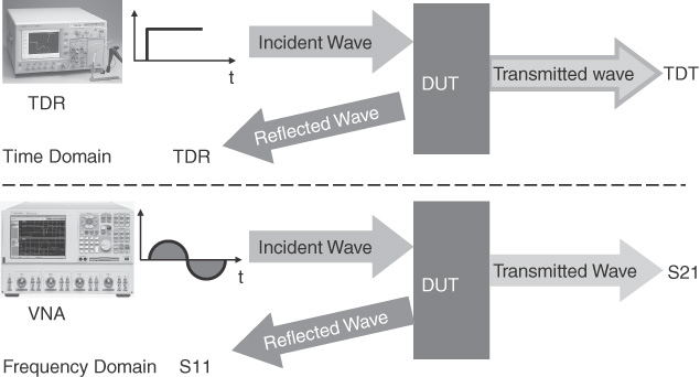
Figure 12-2 S-parameters are a formalism to describe how precision waveforms scatter from an interconnect or a device under test (DUT).
For historical reasons, we use the term scatter when referring to how the waveform interacts. An incident signal can “scatter” off the front of the DUT, back into the source, or it can “scatter” into another connection. The “S” in S-parameters stands for scattering.
We also call the wave that scatters back to the source the reflected wave and the wave that scatters through the device the transmitted wave. When the scattered waveforms are measured in the time domain, the incident waveform is typically a step edge, and we refer to the reflected wave as the time-domain reflection (TDR) response. The instrument used to measure the TDR response is called a time-domain reflectometer (TDR). The transmitted wave is the time-domain transmitted (TDT) wave.
In the frequency domain, the instrument used to measure the reflected and transmitted response of the sine waves is a vector-network analyzer (VNA). Vector refers to the fact that both the magnitude and phase of the sine wave are being measured. On the complex plane, each measurement of magnitude and phase is a vector. A scalar-network analyzer measures just the amplitude of the sine wave, not its phase.
The frequency-domain reflected and transmitted terms are referred to as specific S-parameters, such as S11 and S21, or the return and insertion loss.
This formalism of describing the way precision waveforms interact with the interconnect can be applied to measurements or the output from simulations, as illustrated in Figure 12-3. All electromagnetic simulations, whether conducted in the time domain or the frequency domain, also use the S-parameter formalism.
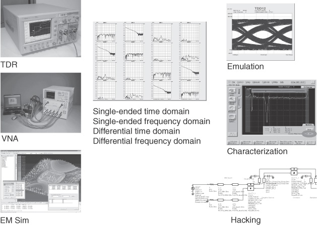
Figure 12-3 Regardless of where the behavioral model comes from, it can be used to emulate system performance, characterize the interconnect, or hack into the performance limitations of the interconnect.
TIP
S-parameters, a formalism developed in the rf world of narrow-band carrier waves, has become the de facto standard format to describe the wide-bandwidth, high-frequency behavior of interconnects in signal-integrity applications.
Regardless of where the S-parameter values come from, they describe the way electrical signals behave when they interact with the interconnect. From this behavioral model, it is possible to predict the way any arbitrary signal might interact with the interconnect, and from this behavior we can predict output waveforms, such as an eye diagram. This process of using the behavioral model to predict a system response is called emulation or simulation.
There is a wealth of information buried in the S-parameters, which describe some of the characteristics of an interconnect, such as its impedance profile, the amount of cross talk, and the attenuation of a differential signal.
With the right software tool, the behavioral measurements of an interconnect can be used to fit a circuit topology−based model of an interconnect, such as a connector, a via, or an entire backplane. With an accurate circuit model that matches physical features with performance, it is possible to “hack” into the model and identify what physical features contribute to the limitations of the interconnect and suggest how to improve the design. This process is popularly called hacking interconnects.
12.3 Basic S-Parameter Formalism
S-parameters describe the way an interconnect affects an incident signal. We use the term port to describe an end where signals enter or exit a device under test (DUT). Ports are connections for both the signal and return paths of the DUT. The easiest way of thinking about a port is as a small coaxial connection to the DUT.
Unless otherwise stated, the impedance the signal sees inside the connection leading up to the DUT is 50 Ohms. In principle, the port impedance can be made any value.
TIP
S-parameters are confusing enough without also arbitrarily changing the port impedances. Unless there is a compelling reason to change them, the port impedances should be kept at 50 Ohms.
Each S-parameter is the ratio of a sine wave scattered from the DUT at a specific port to the sine wave incident to the DUT at a specific port.
For all linear, passive elements, the frequency of the scattered wave will be exactly the same as the incident wave. The only two qualities of the sine wave that can change are the amplitude and phase of the scattered wave.
To keep track of which port the sine wave enters and exits, we label the ports with consecutive index numbers and use these index numbers in each S-parameter.
Each S-parameter is the ratio of the output sine wave to the input sine wave:
The ratio of two sine waves is really two numbers. It is a magnitude that is the ratio of the amplitudes of the output to the input sine waves, and it is the phase difference between the output and the input sine waves. The magnitude of an S-parameter is the ratio of the amplitudes:
While the magnitude of each S-parameter is just a number from 0 to 1, it is often described in dB. As discussed in Chapter 11, the dB value always refers to the ratio of two powers. Since an S-parameter is the ratio of two voltage amplitudes, the dB value must relate to the ratio of the powers within the voltage amplitudes. This is why when translating between the dB value and the magnitude value, a factor of 20 is used:
where:
SdB = value of the magnitude, in dB
Smag = value of the magnitude, as a number
The phase of the S-parameter is the phase difference between the output wave minus the input wave:
As we will see, the order of the waveforms in the definition of the phase of the S-parameter will be important when determining the phase of the reflected or transmitted S-parameter and will contribute to a negative advancing phase.
TIP
While the port assignment of a DUT can be arbitrary, and there is no industry-standardized convention, there should be. If we are using the indices to label each S-parameter, then changing the port assignment index labels will change the meaning of specific S-parameters.
For multiple coupled transmission lines, such as a collection of differential channels, there is one port assignment scheme that is convenient and scalable and should be adopted as the industry standard. It is illustrated in Figure 12-4.

Figure 12-4 Recommended port assignment labeling scheme for multiple transmission-line interconnects. The pattern continues as additional lines are added.
The ports are assigned as an odd port on the left end of a transmission line and the next higher number on the other end of the line. This way, as the number of coupled lines in the array increases, additional index numbers can be added by following this rule. This is a very convenient port assignment approach. S-parameters are confusing enough without creating more confusion with mix-ups in the port assignments.
TIP
You should always try to adopt a port assignment for multiple transmission lines that has port 1 connected to port 2 and port 3 adjacent to port 1, feeding into port 4. This is scalable to n additional transmission lines.
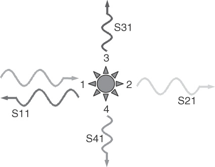
In order to distinguish to which combination of ports each S-parameter refers, two indices are used. The first index is the output port, and the second index is the input port.
For example, the S-parameter for the sine wave going into port 1 and coming out port 2 would be S21. This is exactly the opposite of what you would expect. It would be logical to use the first index as the going-in port and the second number as the coming-out port. However, part of the mathematical formalism for S-parameters requires this reverse-from-the-logical convention. This is related to the matrix math that is the real power behind S-parameters. By using the reverse notation, the S-parameter matrix can transform an array of stimulus-voltage vectors, represented by the vector aj, into an array of response-voltage vectors, bk:
Using this formalism, the transformation of a sine wave into and out of each port can be defined as a different S-parameter, with a different pair of index values. The definition of each S-parameter element is:
This basic definition applies no matter what the internal structure of the DUT may be, as illustrated in Figure 12-5. A signal going into port 1 and coming out port 1 would be labeled S11. A signal going into port 1 and coming out port 2 would be labeled S21. Likewise, a signal going into port 2 and coming out port 1 would be labeled S12.
12.4 S-Parameter Matrix Elements
With only one port on a DUT, there is only one S-parameter, which would be identified as S11. This one element may have many data points associated with it for many different frequency values. At any single frequency, S11 will be complex, so it will really be two numbers. It could be described by a magnitude and phase or by a real component and an imaginary component. This single S-parameter value, at one frequency, could be plotted on either a polar plot or a Cartesian plot.
In addition, S11 may have different values at different frequencies. To describe the frequency behavior of S11, the magnitude and phase could be plotted at each frequency. An example of the measured S11 from a short-length transmission line, open at the far end, is shown in Figure 12-6.

Figure 12-6 Measured S11 as a magnitude (top) and phase (bottom) for a transmission line, open at the far end. Connection was made to both the signal and return path at port 1. Measured with an Agilent N5230 VNA and displayed with Agilent’s ADS.
Alternatively, the S11 value at each frequency can be plotted in a polar plot. The radial position of each point is the magnitude of the S-parameter, and the angle from the real axis is the phase of S11. The positive direction of the angle is always in the counterclockwise (CCW) direction. An example of the same measured S11 but plotted in a polar plot is shown in Figure 12-7.

Figure 12-7 The same measured S11 data as in Figure 12-6 but replotted in a polar plot. The radius position is the magnitude, and the angular position is the phase of S11.
The information is exactly the same in each case but just looks different, depending on how it is displayed. When displayed in a polar plot, it is difficult to determine the frequency values of each point unless a marker is used.
A two-port device would have four possible S-parameters. From port 1, there could be a signal coming out at port 1 and coming out at port 2. The same could happen with a signal going into port 2. The S-parameters associated with the two-port device can be grouped into a simple matrix:
In general, if the interconnect is not physically symmetrical when looking in from each end, S11 will not equal S22. However, for all linear, passive devices, S21 = S12—always. There are only three unique terms in the four-element S-parameter matrix. An example of the measured two-port S-parameters of a stripline transmission line is shown in Figure 12-8.

Figure 12-8 Measured two-port S-parameters of a simple 5-inch-long nearly 50-Ohm stripline transmission line, from 10 MHz to 20 GHz. Shown here are only the magnitude values. There are also phase values for each matrix element and at each frequency point, not shown. Measured with an Agilent N5230 VNA and displayed with Agilent’s PLTS.
This example illustrates part of the power behind the S-parameter formalism. So simple a term as the S-parameter matrix represents a tremendous amount of data. Each of the three unique elements of the 2 × 2 matrix has a magnitude and phase at each frequency value of the measurement, from 10 MHz to 20 GHz, at 10-MHz intervals. This is a total of 2000 × 2 × 3 = 12,000 specific, unique data points, all neatly and conveniently catalog by the S-parameter matrix elements.
This formalism can be extended to include an unlimited number of elements. With 12 different ports, for example, there would be 12 × 12 = 144 different S-parameter elements. However, not all of them are unique. For an arbitrary interconnect, the diagonal elements are unique, and the lower half of the off-diagonal elements is unique. This is a total of 78 unique terms.
In general, the number of unique S-parameter elements is given by:
where:
Nunique = number of unique S-parameter elements
n = number of ports
In this example of 12 ports, there are (12 × 13)/2 = 78 unique elements. Each element has two different sets of data: a magnitude and a phase. This is a total of 156 different plots. If there are 1000 frequency values per plot, this is a total of 156,000 unique data points.
TIP
With this huge amount of data, having a simple formalism to just keep track of the data is critically important.
There are really two aspects of S-parameters. First and most important is the analytical information contained in the S-parameter matrix elements. But there is also information that can be read from the patterns the S-parameter values make when plotted either in polar or Cartesian coordinates. A skilled eye can pick out important properties of an interconnect just from the pattern of the plots.
These S-parameter matrix elements and the data each contains really specify the precise behavior of the interconnect. Everything you ever wanted to know about the behavior of an interconnect is contained in its S-parameter matrix elements. Each S-parameter matrix element tells a different story about the 12-port device. The analytical information these elements contain can be immediately accessed with a variety of simulation tools.
12.5 Introducing the Return and Insertion Loss
In a two-port device, there are three unique S-parameters: S11, S22, and S21. Each of these matrix elements contains complex numbers that may vary with frequency.
The S11 term is also called the reflection coefficient. The S21 term is also called the transmission coefficient.
For historical reasons, the absolute value of the magnitude of the S11, in dB, is called the return loss, and the absolute value of the magnitude of S21, in dB, is called the insertion loss. For example, if S11 = −40 dB, the return loss is 40 dB. If S21 = −15 dB, the insertion loss is 15 dB.
The historical origin of the terms return and insertion loss are based on how these terms were measured before the days of modern VNAs. A fixture would be prepared that could be separated to insert the device under test (DUT). When closed, and with nothing between the two ports, the received signal at port 2 would be measured. The fixture would be separated and the DUT inserted. The loss in what was measured for the through reference, when the DUT was insert, was called the insertion loss—the loss in the transmitted signal when the DUT was inserted.
A large value for insertion loss means much less signal gets to port 2, and the interconnect is not very transparent. Since insertion loss is considered a “loss,” a larger value means there is more loss when the DUT is inserted, and less gets through.
Return loss is measured by first opening the fixture so that port 1 sees an open. The signal reflected from the open is the reference. After the DUT is inserted in the fixture, connecting between port 1 and port 2, the returned signal is measured. The loss in the returned signal, compared with the open, is the return loss.
The better matched the DUT and fixture, the less reflects and the more loss in the reflected signal compared with the reference open. A large return loss means a good match compared to an open. A small return loss means a lot of signal is reflecting, and it is looking like a really big impedance mismatch from the 50-Ohm port, so that it looks more like an open or a short.
Even though these terms were introduced long before VNAs, they are still used when referring to S11 and S21, though they carry a lot of confusion. Many of us in the industry have adapted the bad habit of using return loss as a substitute for S11 and the insertion loss as a substitute for S21. This is not technically correct, even though it’s incredibly convenient.
When insertion loss increases, for example, and there is less received signal, the transmission coefficient decreases, and S21 decreases. The S21 value becomes a larger, more negative dB value. When we say the insertion loss is increasing, do we mean there is a decreasing transmission coefficient or an increasing transmission coefficient? Likewise, for return loss. When return loss is large, this means there is very little signal reflected, and the DUT is a good match to the fixture. If return loss increases, does this mean the reflection coefficient increases or the reflection coefficient decreases?
Some in the industry advocate changing the definition of return and insertion loss and have them mean precisely the magnitude of S11 and S21, in dB. This would remove the ambiguity. In this context, a larger return loss means a larger reflection coefficient and a larger S11 and more signal reflects. A smaller insertion loss means a smaller transmission coefficient and a smaller S21 and fewer signal transmits. While technical, if not historically, correct, this usage dramatically reduces the confusion associated with S-parameters. Given how many confusing aspects there are, this is not a bad idea.
TIP
Throughout this book, we adopt the growing consensus definition that the insertion loss is the same as S21 and the return loss is the same as S11. Although doing so removes one source of confusion, it introduces another.
TIP
It is always unambiguous to refer to S11 as the reflection coefficient and S21 as the transmission coefficient. A more transparent interconnect will have a smaller reflection coefficient and a larger transmission coefficient. This is exactly the opposite directions from the historically correct return and insertion loss terms.
When the interconnect is symmetrical from one end to the other, the return losses, S11 and S22, are equal. In an asymmetric two-port interconnect, S11 and S22 will be different.
In general, calculating by hand the return and insertion loss from an interconnect line is complicated. It depends on the impedance profile and time delays of each transmission-line segment that makes up the interconnect and the frequency of the sine waves.
In the frequency domain, any response to the sine waves is at steady state. The sine wave is on for a long time, and the total reflected or transmitted response is observed. This is an important distinction between the frequency domain and the time domain.
In the time domain, the instantaneous voltage reflected or transmitted by the transmission line is observed. The reflected response, the TDR response, can map out the spatial impedance profile of the interconnect by looking at when a reflection occurred and where the exciting edge must have been when the reflection happened. Of course, after the first reflection, an accurate interpretation of the impedance profile can be obtained only by post processing the reflected signal, but a good first-order estimate can always be read directly from the TDR response.
In the frequency domain, the spatial information is intermixed throughout the frequency-domain data and not directly displayed. Consider an interconnect with many impedance discontinuities down its length, as shown in Figure 12-9.
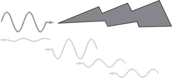
Figure 12-9 Each arbitrary impedance discontinuity in the irregularly shaped interconnect causes a reflected sine wave back to the incident port, each with a different magnitude and phase.
As the incident sine wave encounters each discontinuity, there will be a reflection, and some of the sine wave will head back to the port. Some of the reflected waves will bounce multiple times between the discontinuities until they either are absorbed or eventually make it out to one of the ports where they are recorded.
What is seen as the reflected signal from port 1, for example, is the combination of all the reflected sine waves from all the possible discontinuities. For an interconnect 1 meter long, the typical time for a reflection down and back is about 6 nsec. In the 1 msec, a typical time for a VNA to perform one frequency measurement, a sine wave could complete more than 100,000 bounces, far more than would ever occur.
TIP
For any single frequency, the reflected signal or transmitted signal is a steady-state value. It represents all the possible combinations of reflections at all the different impedance interfaces. This is very different from the behavior in the time domain.
If the frequency incident to the port is fixed during the 1-msec measurement or simulation time, the frequency of every wave reflecting back from every discontinuity will be exactly the same frequency. However, the amplitude and phase of each resulting wave exiting the interconnect at each port will be different.
Coming out of each port will be a large number of sine waves, all with the same frequency but with an arbitrary combination of amplitudes and phases, as illustrated in Figure 12-10. Surprisingly, when we add together an arbitrary number of sine waves, each with the same frequency but with arbitrary amplitude and phase, we get another sine wave.

Figure 12-10 The sum of a large number of sine waves, all with the same frequency but different amplitudes and phase, is another sine wave.
When a sine wave is incident into one of the ports, the resulting signal that comes back out one of the ports is also a sine wave of exactly the same frequency but with a different amplitude and phase. This is what is captured in the S-parameters. Unfortunately, other than in a few special cases, the behavior of the S-parameters is a complicated function of the impedance profile and sine wave frequency. It is not possible to take the measured magnitude and phase of any S-parameter and back out each individual sine wave element that created it.
In general, other than in a few simple cases, it is not possible to calculate the S-parameters of an interconnect by hand with pencil and paper. A simulator must be used. Though there are a number of sophisticated, commercially available simulators that can simulate the S-parameters of arbitrary structures, any SPICE simulator can calculate the return and insertion loss of any arbitrary structure with a simple circuit, as illustrated in Figure 12-11. An example of an interconnect with a few discontinuities is also shown.
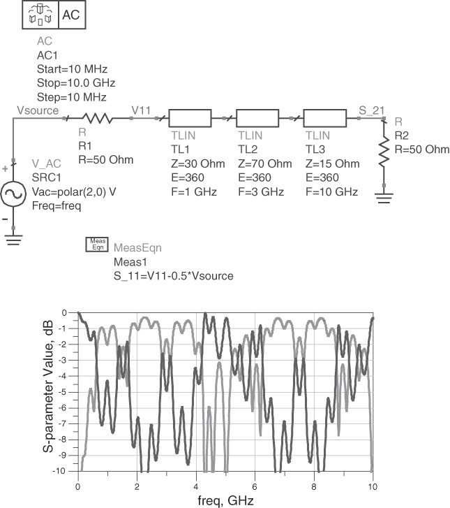
Figure 12-11 SPICE circuit to calculate the S11 and S21 of any interconnect circuit between the ports. Circuit set up in Agilent’s ADS version of SPICE.
While any arbitrary interconnect can be simulated, there are a few important patterns in the S-parameters that are indicative of specific features in the interconnect. Learning to recognize some of these patterns will enable the trained observer to immediately translate S-parameters into useful information about the interconnect.
One important pattern to recognize is that of a transparent interconnect. The pattern of the return and insertion loss can immediately indicate the “quality” of the interconnect as “good” or “bad.” In this context, we assume that “good” means the interconnect is transparent to signals, and “bad” means it is not transparent to signals.
12.6 A Transparent Interconnect
There are three important features of a transparent interconnect:
1. The instantaneous impedance down the length matches the impedance of the environment in which it is embedded.
2. The losses through the interconnect are low, and most of the signal is transmitted.
3. There is negligible coupling to adjacent traces.
These three features are clearly displayed at a glance in the reflected and transmitted signals, which correspond to the S11 and S21 terms, when the ports are attached to opposite ends of the interconnect, labeled port 1 and port 2.
Examples of the port configuration and measured return and insertion loss for a nearly transparent interconnect are shown in Figure 12-12.

Figure 12-12 Measured return and insertion loss of a nearly transparent interconnect. Measured with an Agilent N5230 VNA and displayed with Agilent’s ADS.
When the impedance throughout the interconnect closely matches the port impedances, very little incident signal reflects, and the reflected term, S11, is small. When displayed in dB, a smaller return loss is a larger, more negative dB value. The 50-Ohm impedance of port 2 effectively terminates the interconnect.
Of course, in practice, it is almost impossible to achieve a perfect match to 50 Ohms over a large bandwidth. Typically, the measured reflection coefficient of an interconnect gets larger at higher frequency, as shown in Figure 12-12 as a smaller negative dB value at higher frequency.
When displayed as a dB value, a transparent interconnect will have a large negative dB reflection coefficient and a small S11. Using the modern term, we would say the return loss is small.
The worse the interconnect and the larger the impedance mismatch to the port impedances, the closer the return loss will be to 0 dB, corresponding to 100% reflection.
The insertion loss is a measure of the signal that transmits through the device and out port 2. The larger the impedance mismatch, the less transmitted signal. However, when there is close to a good match, the insertion loss is very nearly 0 dB and is insensitive to impedance variations.
There is a specific connection between the reflection coefficient and the transmission coefficient. Always keep in mind that the S-parameters are ratios of voltages. There is no law of conservation of voltage, but there is a law of conservation of energy.
If the interconnect is low loss, and there is no coupling to adjacent traces, and there is no radiated emissions, then the energy into the interconnect must be the sum of the reflected energy and the transmitted energy.
The energy in a sine wave is proportional to the square of its amplitude. This condition of energy in being equal to the energy reflected plus the energy transmitted is described by:
Given the return loss, the insertion loss is:
For example, if the impedance somewhere on the interconnect is 60 Ohms in an otherwise 50-Ohm environment, the worst-case return loss would be:

The impact on insertion loss is:
Even though the return loss is as high as −20 dB, the impact on insertion loss is very small and indistinguishable from 0 dB. Figure 12-13 illustrates this for a wide range of return loss values.

Figure 12-13 Impact on the insertion loss for different return losses. The return loss must be as high as −10 dB for there to be even a 0.5-dB impact on the insertion loss if there are no losses in the interconnect.
TIP
Only for a return loss higher than −10 dB will there be a noticeable impact on the insertion loss.
12.7 Changing the Port Impedance
The industry-standard port impedance is 50 Ohms. However, in principle, it can be made any value. As the port impedance changes, the behavior of the displayed return and insertion loss changes. To first order, moving the port impedance farther from the interconnect’s characteristic impedance will increase the return loss. Other than this simple pattern, the specific values of the return loss and insertion loss are complicated functions of the port impedance.
Given the S-parameters at one port impedance, the S-parameters with any other port impedance can be calculated using matrix math. They can also be calculated directly in a SPICE circuit simulation.
To describe the S-parameters of an interconnect, it is not necessary to match the port impedance to the impedance of the device. Unless there is a compelling reason otherwise, 50 Ohms should always be used.
Regardless of the port impedance, an analytical analysis of each S-parameter element can be equally well performed. The only practical reason to switch the port impedance from 50 Ohms is to be able to qualitatively evaluate, from the front screen, the quality of the device in a non-50-Ohm environment.
If the device, like a connector or cable, is designed for a non-50-Ohm application, like the 75-Ohm environment of cable TV applications, its return loss will look “bad” when displayed with 50-Ohm port impedances.
The reflections from the impedance mismatches at the ends will cause ripples in the return loss. The excessive return loss will show ripples in the insertion loss. To the trained eye, the behavior will look complicated and will be difficult to interpret, other than that the impedance is way off from 50 Ohms.
But if the application environment were 75 Ohms, the interconnect might be acceptable. By changing the port impedance to 75 Ohms, the application impedance, the behavior of the device in this application environment can be visually evaluated right from the front screen.
An example of the return loss and insertion loss of a nominally 75-Ohm transmission line with 50-Ohm connectors attached is shown in Figure 12-14 for the case of 50-Ohm and 75-Ohm port impedances.

Figure 12-14 Measured return and insertion loss for a 75-Ohm transmission line with 50-Ohm connectors using port impedances of 50 Ohms and 75 Ohms. Measured with an Agilent N5230 VNA and displayed with Agilent’s ADS.
In a 75-Ohm environment, the 75-Ohm cable looks nearly transparent at low frequency, below about 1 GHz. Above 1 GHz, the connectors dominate the behavior, and the interconnect is not very transparent, no matter what the port impedance. The behavioral model contained in the measured S-parameter response is exactly the same, regardless of the port impedances. It is merely redisplayed for different port impedances.
S-parameters are confusing enough without also leaving the port impedance ambiguous. Of course, when the S-parameters are stored in the industry-standard touchstone file format, the port impedances of each port to which the data is referenced are specifically called out at the top of the file. From one touchstone file, the S-parameters for any port impedance can easily be calculated.
12.8 The Phase of S21 for a Uniform 50-Ohm Transmission Line
The simplest interconnect to evaluate is when the impedance of the line is 50 Ohms, matched to the impedance of the ports. In this case, there are no reflections, and the magnitude of S11 is 0. In dB, this is a large, negative dB, usually limited by the noise floor of the instrument or simulator, on the order of −100 dB.
All of the sine wave would be transmitted so the magnitude of S21 would be 1, which is 0 dB at each frequency. The phase of S21 would vary depending on the time delay of the transmission line and the frequency. The behavior of the phase is one of the most subtle aspects of S-parameters.
The definition of the S-parameters is that each matrix element is the ratio of the sine wave that comes out of a port to the sine wave that goes into a port.
For S21, the ratio of the sine wave coming out of port 2 to the sine wave going into port 1, we get two terms:
When we send a sine wave into port 1, it doesn’t come out of port 2 until a time delay, TD, later. If the phase is 0 degrees when the sine wave went into port 1, it will also have a phase of 0 degrees when it comes out of port 2. It has merely been transmitted from one end of the line to the other.
However, when we compare the phase of the sine wave coming out of port 2 to the phase of the sine wave going into port 1, it is the phases that are present at the same instant of time. This is illustrated in Figure 12-15.

Figure 12-15 Phase of S21 is negative due to the incident phase advancing while the sine wave is transmitting through the transmission line.
When we see the 0-degree phase sine wave coming out of port 2 and then immediately look at the phase of the wave going into port 1, we are looking not at the 0-degree phase when the sine wave entered the transmission line TD nsec ago but at the current phase of the sine wave entering port 1 now.
During the time the 0-degree wavefront has been propagating through the transmission line, the phase of the sine wave entering port 1 has advanced. The phase of the sine wave entering port 1 is now f × TD.
When we calculate the phase of S21 as the difference between the phase coming out of port 2 minus the phase going into port 1, the phase coming out of port 2 may be 0 degrees, but the phase going into port 1 now has advanced to f × TD. This means the phase of S21 is:
where:
f = frequency of the sine wave going into port 1
TD = time delay of the transmission line
TIP
The phase of S21 will start out negative and will become increasingly negative with frequency. This is the most bizarre and confusing aspect of S-parameters: The phase of S21 through a transmission line is increasingly negative.
We see that this behavior is based on two features. First, the definition of the phase of S21 is that it is the phase of the sine wave coming out of port 2 minus the phase of the sine wave going into port 1. Second, it is the difference in phase between the two waves at the same instant in time. The phase of S21 will always be negative and will become increasingly negative as frequency increases. An example of the measured phase of S21 for a stripline transmission line is shown in Figure 12-16.

Figure 12-16 Measured phase of S21 for a uniform, 50-Ohm stripline, about 5 inches long, measured from 10 MHz to 5 GHz. Measured with an Agilent N5230 VNA and displayed with Agilent’s PLTS.
At low frequency, the phase of S21 starts out very nearly 0 degrees. After all, if the TD is small compared to a cycle, then the phase does not advance very far during the transit time of the wave through the interconnect. As frequency increases, the number of cycles the sine wave advances during the transit time increases. Since the phase of S21 is the negative of the incident phase, as the incident phase advances, the phase of S21 gets more and more negative.
We usually count phase from −180 degrees to +180 degrees. When the phase advances to −180, it is reset to +180 and continues to count down. This gives rise to the typical sawtooth pattern for the phase of S21.
12.9 The Magnitude of S21 for a Uniform Transmission Line
The magnitude of the insertion loss is a measure of all the processes that prevent the energy being transmitted through the interconnect. The total energy flowing into an interconnect must equal the total energy coming out. There are five ways energy can come out:
1. Radiated emissions
2. Losses in the interconnect turning into heat
3. Energy coupled into adjacent traces, whether measured or not
4. Energy reflected back to the source
5. Energy transmitted into port 2 and measured as part of S21
In most applications, the impact on S21 from radiated losses is negligible. Though radiated emissions are an important factor in causing FCC certification test failures, the amount of energy typically radiated is so small a fraction of the signal as to be difficult to detect in S21.
The losses in the interconnect that turn into heat are accounted for by the conductor loss and dielectric loss. As shown in Chapter 11, both of these effects increase monotonically with frequency. When all other mechanisms that affect S21 are eliminated, when measured in dB, the insertion loss is a direct measure of the attenuation in the line and will increase as a more negative dB value with increasing frequency. Figure 12-17 shows the measured insertion loss of a stripline transmission line about 5 inches long.

Figure 12-17 Measured insertion loss of 5-inch-long stripline. Measured with an Agilent N5230 VNA and displayed with Agilent ADS.
There is often some ambiguity around the sign of the attenuation. Usually, when describing the attenuation, the sign chosen is positive because a larger attenuation should be a larger number. In this formalism, attenuation is not the same as the transmission coefficient. There is a sign difference between them. If the only energy loss mechanism is from attenuation, the historical term insertion loss would be the same as attenuation.
The transmission coefficient is the negative of the attenuation. When attenuation is described by the insertion loss and measured in dB, it is critically important to be absolutely consistent and always make the insertion loss the correct—negative—sign.
TIP
Insertion loss is a direct measure of the attenuation from both the conductor and dielectric losses. Given the conductor and dielectric properties of the transmission line, as described in Chapter 9, the insertion loss can be easily calculated.
The insertion loss due to just the losses is:
where:
S21 = insertion loss, in dB
Adiel = attenuation from the dielectric loss, in dB
Acond = attenuation from the conductor loss, in dB
When there are no impedance discontinuities in the transmission lines, and conductor loss is small compared to the dielectric loss, the insertion loss is a direct measure of the dissipation factor:
where:
S21 = insertion loss, in dB
f = frequency, in GHz
Df = dissipation factor
Dk = dielectric constant
Len = interconnect length, in inches
A measurement of the insertion loss, when scaled appropriately, is a direct measure of the dissipation factor of the laminate material:
S21 = insertion loss, in dB
f = frequency, in GHz
Df = dissipation factor
Dk = dielectric constant
Len = interconnect length, in inches
When the dielectric constant is close to 4, which is typical for most FR4 type materials, the insertion loss is approximated as −5 × Df dB/inch/GHz. Figure 12-18 shows the same measured insertion loss for the stripline case above but scaled by 5 and by the length and frequency to plot the dissipation factor directly.

Figure 12-18 Measured FR4 stripline insertion loss replotted as dissipation factor, showing the value of about 0.022. The higher values at low frequency are due to conductor losses not taken into account. Measured with an Agilent N5230 VNA and displayed with Agilent ADS.
At low frequency, conductor loss can be a significant contributor to loss and is not taken into account in this simple analysis of insertion loss. When the approximation above is used and all the attenuation is assumed to be dielectric loss, the extracted dissipation may be artificially higher, compensating for the conductor loss. At higher frequency, the impedance discontinuities, typically from connectors or vias, cause ripples in the insertion loss.
While the slope of the insertion loss per length is a rough indication of the dissipation factor of an interconnect, it is only a rough indication. In practice, the discontinuities from impedance discontinuities of both the impedance of the line and from the connectors, as well as from contributions to the attenuation from the conductor losses will complicate the interpretation of the insertion loss. In general, for accurate measurements of the dissipation factor, these features must be taken into account.
However, the behavior of the insertion loss is a good indicator of dissipation factor of the materials. Figure 12-19 shows an example of the measured insertion loss for two nearly 50-Ohm transmission lines, each about 36 inches long. One is made from a Teflon substrate, while the other is made from FR5, a very lossy dielectric. The much larger slope of the FR5 substrate is an indication of this much higher dissipation factor.

Figure 12-19 Measured FR5 and Teflon transmission lines, showing the impact on the insertion losses from the dissipation factors of the laminates. Each line is a 50-Ohm microstrip and 36 inches long. Measured with an Agilent N5230 VNA and displayed with Agilent ADS.
When plotted as a function of frequency, the insertion loss shows a monotonic drop in magnitude. At the same time, the phase is advancing at a constant rate in the negative direction. When S21 is plotted in a polar plot, the behavior is a spiral, as shown in Figure 12-20.

Figure 12-20 Measured insertion loss of the 36-inch-long FR5 micro-strip from Figure 12-19 but plotted in a polar plot. The frequency range is 10 MHz to 2 GHz, measured every 10 MHz. Measured with an Agilent N5230 VNA and displayed with Agilent ADS.
The lowest frequency has the largest magnitude of S21 and a phase close to zero. As frequency increases, S21 rotates around in the clockwise direction, with smaller and smaller amplitude. It spirals into the center.
The spiral pattern of the insertion loss of a uniform transmission line, or the return loss when looking at the one-port measurement of a transmission line open at the end, is a pattern indicative of losses in the line that increase with frequency, which is typical of conductor and dielectric losses.
12.10 Coupling to Other Transmission Lines
Even if the cross-talk noise into adjacent lines is not measured, it will still happen, and its impact will be the magnitude reduction of S11 and S21. The simplest case is a uniform microstrip line with an adjacent microstrip closely coupled to it.
The insertion loss of an isolated microstrip will show the steady drop-off due to the dielectric and conductor loss. As an adjacent microstrip is brought closer, some of the signal in the driven microstrip will couple into the adjacent one, giving rise to near- and far-end cross talk. In microstrip, the far-end noise can be much higher than the near-end noise.
If the ends of the adjacent microstrip are also terminated at 50 Ohms, then any cross talk will effectively be absorbed by the terminations and not reflect in the victim microstrip line.
As frequency increases, the far-end cross talk will increase, and more signal will be coupled out of the driven line, reducing S21. In addition to the drop in S21 from attenuation, there will also be a drop in S21 from cross talk. As the two traces are brought closer together and coupling increases, more energy flows from the active line to the quiet line, and less signal makes it out as S21. Figure 12-21 shows that S21 will decrease with frequency and with coupling as the spacing between the lines decreases.

Figure 12-21 The insertion loss of one line in a microstrip pair. As the coupling increases, energy is coupled out of the line, and S21 decreases more than just due to attenuation. Simulated with Agilent’s ADS.
TIP
Just looking at the S21 response, it is difficult to separate out how much of S21 is due to attenuation and how much is due to coupling to other interconnects, unless the coupled signal into the other interconnects is also measured.
Using the standard port-labeling convention, two adjacent microstrip lines can be described by four ports. The insertion loss of one line is S21, while the insertion loss of the other line is S43. The near-end noise is described by S31 and the far-end noise by S41. As the coupling increases and S21 drops, we can see the corresponding increase in the far-end noise, S41, as shown in Figure 12-22.

Figure 12-22 Insertion loss, S21, of one line in a microstrip pair and the far-end cross talk, S41, showing the insertion loss decreasing as the far-end noise increases. Simulated with Agilent ADS.
In this example, the reduction in magnitude of S21 from coupling increased with frequency but was relatively slowly varying. When the coupling is to an interconnect that is not terminated but is floating, the Q of the isolated floating line can be very high. If it were excited, the noise injected would rattle around between the open ends, attenuating slightly with each bounce. It could rattle around for as many as 100 bounces before eventually dying out from its own losses.
The impact from coupling to high-Q resonators is very narrow-band absorption in S21 or S11. Figure 12-23 shows the S21 of the same microstrip as above, but now the adjacent victim line is floating, open at each end. It has very narrow frequency resonances, which suck out energy in the active line in a very narrow frequency range at the line resonance frequency.

Figure 12-23 The insertion loss of a microstrip line when a floating adjacent microstrip line is very far away and when it is closely spaced. When close, the high-Q resonance of the floating line couples energy in narrow frequency bands. Simulated with Agilent ADS.
Coupling to high-Q resonators is also apparent when measuring the return loss in one-port configurations. In principle, when one port is connected to a transmission line with its other end open, S11 should have a magnitude of 1, or 0 dB. In practice, as we have seen, all interconnects have some loss, so S11 is always smaller than 0 dB, and it continues to get smaller as frequency increases.
If there is coupling between the transmission line being measured and adjacent transmission lines that are unterminated, the lines will act as high-Q resonators and show very narrow absorption lines.
Narrow, sharp dips in the return or insertion loss are almost always indications of coupling to high-Q resonant structures. When the resonating structure has a complex geometry, the multiple resonant frequency modes may be difficult to calculate without a full-wave field solver.
In the case of a single adjacent transmission line, the frequency of the dip is the resonant frequency of the quiet line. The width of the resonance is related to the Q of the resonator. By definition, the Q is given by:
where:
Q = value of the quality of the resonance
fres = resonant frequency
FWHM = full width, half minimum (the frequency width across the dip at half the minimum value)
The higher the Q, the narrower the frequency dip. The depth of the dip is related to how tight the coupling is. With a larger coupling, the dip will be deeper. Of course, as the dip gets deeper, the coupling to the floating line increases, and its damping generally increases, causing the Q to decrease.
The resonator to which a signal line couples does not have to be another uniform transmission line but can be the cavity made up of two or more adjacent planes. For example, when a signal transitions from one layer to another and its return plane also changes, the return current, transitioning between the return planes, can couple into the cavity, creating high-Q resonant couplings. An example of this layer transition in a four-layer board is shown in Figure 12-24.

Figure 12-24 A signal transitions two reference planes, layer 1 and layer 2. The return current, flowing between the two planes, couples into the plane cavity resonance.
The resonant frequency of a cavity composed of two planes is the frequency where an integral number of half-wavelengths can fit between the two open ends of the cavity. It is given by:
where:
fres = resonant frequency, in GHz
Dk = dielectric constant of the laminate inside the cavity = 4
Len = length of a side of the cavity, in inches
n = index number of the mode
11.8 = speed of light in vacuum in inches/nsec
For example, when the length of a side is about 1 inch, the resonant frequency with an FR4 laminate begins at about 3 GHz and increases from there for higher modes. In real cavities, the resonant frequency spectrum can be more complex due to cutouts in the planes or rectangular shapes.
In typical board-level applications, the length of a side can easily be 10 inches, with a resonant frequency starting at about 300 MHz. In this range, the decoupling capacitors between power and ground planes can sometimes suppress resonances or shift them to higher frequency, and the resonances may not be clearly visible.
However, in multilayer packages, typically on the order of 1 inch on a side, the first resonances are in the GHz range, and the decoupling capacitors are not effective at suppressing these modes since their impedance at 1 GHz is high compared to the plane’s impedance. When a signal line transitions from the top layer to a bottom layer, going through the plane cavity, the return current will excite resonances in the GHz range.
This can easily be measured by using a one-port network analyzer. Figure 12-25 shows the measured return loss of six different leads in a four-layer BGA. In each case, the signal line is measured at the ball end, and the cavity end—where the die would be—is left open. Normally, the return loss should be 0 dB, but at the resonant frequencies of the cavity, a considerable amount of energy is absorbed.

Figure 12-25 The measured return loss of six different leads in a BGA package, each open at the far end. The dips starting at 1 GHz are resonances in the cavity formed by the power and ground planes, as well as coupling into adjacent signal lines. Measured with an Agilent N5230 VNA and displayed with Agilent ADS.
In this example, the return loss drops off very slowly from 0 dB as frequency increases due to the dielectric loss in the laminate. Above about 1 GHz, there are very large, narrow bandwidth dips. These are the absorptions from coupling into the power and ground cavity of the package.
If the return loss from a reflection at the open source is −10 dB, which is from a round-trip path, the drop in the one-way insertion loss might be on the order of −5 dB. When the magnitude is −5 dB, this means that only 50% of the signal amplitude would get through. This is a huge reduction in signal strength and would result in distortions of the signal as well as excessive cross talk between channels.
The return loss is really a measure of the absorption spectrum of the package, similar to an infrared absorption spectrum of an organic molecule. Infrared spectroscopy identifies the distinctive resonant modes of specific atomic bonds. In the same way, these high-Q package resonances identify specific resonant modes of the package or component.
Not only can the plane cavities absorb energy, but other adjacent traces can act as resonant absorbers. The resonant absorptions of a package will often set the limit to its highest usable frequency. One of the goals in package design is to push these resonances to higher frequency or reduce the coupling of critical signal lines to the resonant modes. This can be accomplished in a number of ways:
• Don’t transition the signal between different return planes.
• Use return vias adjacent to each signal via to suppress the resonance.
• Use low-inductance decoupling capacitors to suppress the resonances.
• Keep the body size of the package very small.
12.11 Insertion Loss for Non-50-Ohm Transmission Lines
When the losses are small and coupling out of the line to adjacent lines is small, the dominant mechanism affecting the insertion loss is reflections from impedance discontinuities. The most common source of discontinuity is when the transmission line is different from the 50 Ohms of the ports. The impedance mismatch at the front of the line and the end of the line will give rise to a type of resonance, causing a distinctive pattern to the return and insertion loss.
Consider the case, as illustrated in Figure 12-26, of a short length of lossless transmission line. It has a characteristic impedance Z0, different from 50 Ohms, and a time delay, TD. The port impedances are 50 Ohms. As the sine wave hits the transmission line, there will be a reflection at the front interface, sending some of the incident sine wave back into port 1, contributing to the return loss. However, most of the incident sine wave will continue through the transmission line to port 2, where it will reflect from that interface.

Figure 12-26 Multiple reflections from the interfaces through a non-50-Ohm, uniform transmission line.
The reflection coefficient for a signal traveling from port 1 into the transmission line, rho1, is:

Once the signal is in the transmission line, when it hits port 2 or port 1, the reflection coefficient back into the line, rho, will be:

where:
rho1 = reflection coefficient from port 1 to the transmission line
rho = reflection coefficient from the line into port 1 or port 2
Z0 = characteristic impedance of the transmission line
Whatever the phase shift off the reflection from the first interface, the phase shift from the reflection off the second interface will be the opposite. The phase shift propagating a round-trip distance down the interconnect and back is:
where:
Phase = phase shift of the reflected wave, in degrees
TD = time delay for one pass through the transmission line
f = sine wave frequency
If the round-trip phase shift is very small, the reflected wave from the end of the line when it enters port 1 will have nearly equal magnitude but opposite phase from the reflected signal off port 2. As the wave heads back into port 1, the signals will cancel, and the net reflected signal into port 1 will be 0.
TIP
At low frequency, the return loss of all lossless interconnects will always start at very little reflecting, or a very large negative dB value.
If nothing reflects back into port 1, then everything must be transmitted into port 2. and the insertion loss of all lossless interconnects will start at 0 dB. This is due to the second reflected wave back toward port 2 having the same phase as the first wave into port 2, and they both add.
TIP
At low frequency, the insertion loss of all lossless interconnects will always start at 0 dB.
As the frequency increases, the round-trip phase shift of the transmitted signal will increase until it is exactly half a cycle. At this point, the reflected signal from the front interface heading into port 1 will be exactly in phase with the reflected signal from the back interface, heading into port 1. They will add in phase, and the return loss will be a maximum. The return loss will be:
If S11 is a maximum, the insertion loss will be a minimum. When the round-trip phase shift is 180 degrees, the second reflected wave heading back to port 2 will be 180 degrees out of phase with the first wave heading into port 2, and they will partially cancel out.
As frequency increases, the round-trip phase will cycle between 0 and 180, causing the return and insertion losses to cycle between minimum and maximum values.
Dips in return loss and peaks in insertion loss will occur when the round-trip phase is a multiple of 360 degrees, or Phase = n × 360. This occurs when:
or:
The longer the time delay, TD, the shorter the spacing between frequency intervals for a 180-degree phase shift. An example of the return and insertion loss for two 30-Ohm transmission lines, with a TD of 0.5 and 0.1 nsec, is shown in Figure 12-27. The frequency intervals between dips should be 1 GHz and 5 GHz, respectively.

Figure 12-27 The return and insertion loss for two 30-Ohm, lossless, uniform transmission lines with TD of 0.5 nsec and 0.1 nsec. The longer the time delay, the shorter the interval between dips. Simulated with Agilent’s ADS.
A glance at the frequency interval between the ripples in the return or insertion loss can give a good indication of the physical length between the discontinuities of a transmission-line interconnect. The TD of the interconnect is roughly:
where:
TD = interconnect time delay
Δf = frequency interval between dips in the return loss or peaks in insertion loss
For example, in the return-loss plot at the top of Figure 12-27, the frequency spacing between dips in one transmission line is 1 GHz. This corresponds to a time delay of the interconnect of about 1/(2 × 1) = 0.5 nsec.
TIP
The best way to make a transparent interconnect is first to match the interconnect impedance to 50 Ohms. If you can’t make the impedance 50 Ohms, then the next most important design guide is to keep it short.
Interposers between a semiconductor package and a circuit board are designed to be transparent. When their impedance is far off from 50 Ohms, the design guideline to keep them transparent is to keep them short. This condition is that:
If the wiring delay of an interconnect is roughly 170 psec/inch, then the maximum length of a transparent interposer is given by:
or:
If we translate the << condition to be 10x, then this rough rule of thumb becomes:
where:
Len = interposer length in inches
fmax = maximum usable frequency where the interconnect is still transparent, in GHz
For example, if the operating frequency is 1 GHz, an interposer or a connector should be shorter than about 0.3 inches to still be transparent. Likewise, if an interposer is 10 mils long, it could have a usable bandwidth of 30 GHz without any other special design conditions.
An example of a compliant interposer from Paricon, about 10 mils thick and with a 30-GHz bandwidth, is shown in Figure 12-28.
Figure 12-28 Cross section of the Pariposer interposer from Paricon, which is about 10 mils thick and has a bandwidth in excess of 30 GHz.
Of course, if the interconnect is designed as a controlled-impedance path with a characteristic impedance near 50 Ohms, it can have a much higher bandwidth and can be much longer.
12.12 Data-Mining S-Parameters
The interpretation of the S-parameter elements depends on the port assignments. For example, a semiconductor package could have 12 different traces, one end of each trace connected to a port, and every trace open at its far end. Or there could be one net on a board with a fanout of 11 and a port at each end of the single net. Or the port assignment could be as shown in Figure 12-29, with six different straight-through interconnects in some proximity. These six different transmission lines could be grouped in pairs to create three different differential channels.

Figure 12-29 The index labeling for a 12-port device, which could be three differential channels. Not shown are the return paths, but they are assumed to be present and connected to the ports.
The precise internal connections to the device will influence how to interpret each S-parameter. The most common case is with the six different through connections with port assignments as shown. Always remember that if the port assignments change, the interpretation of each specific S-parameter will change as well.
With 12 ports, there will be a total of 78 unique S-parameter elements, each having a magnitude and phase and each varying with frequency.
The diagonal elements are the return losses of each transmission line and have information about impedance changes in the interconnect. If the lines are all similar and symmetrical, all of the diagonal elements could be the same.
The six unique, direct through signals, the insertion losses S21, S43, S65, S87, S10,9, and S12,11 have information about the losses, the impedance discontinuities, and even resonances from stubs. All the other S-parameter elements represent coupling terms, containing information about cross talk. For example, S51, the ratio of a sine wave coming out of port 5 to the sine wave going into port 1, is related to the near-end cross talk between lines two away. The S61 term has information about the far-end cross talk between lines far away.
Of course, the near-end noise between the first line and each of the adjacent signal lines will drop off with spacing. Figure 12-30 is an example of the simulated near-end noise from one line to five other adjacent lines, each 5 mils in width and spaced 7 mils to the adjacent trace, each being 10 inches long.

Figure 12-30 Near-end cross talk from one line to five adjacent microstrip lines, each 10 inches long, with spacing between them of 7 mils. The farther away the line, the lower the near-end cross talk. Simulated with Agilent’s ADS.
Though the near-end noise between adjacent lines, S31, may be −25 dB, the near-end noise to the line five lines away, S11,1, is less than −55 dB.
TIP
Everything you ever wanted to know about the electrical behavior of interconnects is contained in their S-parameters.
So far, we have considered the signals into the ports as single-ended sine wave signals. Two other types of signals provide an alternative description of the stimulus-response behavior, which can often provide valuable insight into the behavior of the interconnects. Depending on the specific question being asked, these other forms may offer a faster route to the correct answer.
The two other forms of the S-parameters are differential and time domain.
12.13 Single-Ended and Differential S-Parameters
Two independent transmission lines in proximity and with coupling can be described in two equivalent ways. On the one hand, they are two independent transmission lines, each with independent properties. For example, if we use the labeling scheme suggested in the preceding section, where port 1 goes through to port 2 and port 3 goes through to port 4, each transmission line would have reflected elements, S11 and S33, and each would have a transmitted element, S21 and S43.
In addition, there would be cross talk between the two lines, the unique near end would be S31 and S42, and the unique far-end terms would be S41 and S32. The near- and far-end noise signatures would vary depending on the spacing, coupling lengths, and whether the topology were stripline or microstrip. All the electrical properties of these two transmission lines are completely described by these 10 unique S-parameter elements across the frequency range.
These same two lines can also be described as one differential pair. No assumptions have to be made about the lines; this description as a differential pair is a complete description. But, the words we use and the sorts of behavior we describe are very different for a single differential pair description than for two independent single-ended transmission lines with coupling.
TIP
When the S-parameters are describing the differential properties of the interconnects, we refer to the S-parameters as the differential S-parameters or the mixed-mode S-parameters or the balanced S-parameters. These terms are used interchangeably in the industry. The preferred term is mixed-mode S-parameters.
Using mixed-mode S-parameters, we describe the four-port interconnect in terms of being a differential pair, in which case we refer to the ports as differential ports. With one differential pair and a differential port on either end, the only types of signals that exist are differential signals and common signals. Any arbitrary waveform going into either of the differential ports can be described by a combination of differential and common signals.
These signals are often called the differential mode and common mode signals. Using this terminology is a bad habit. There is no need to invoke the word mode. The signals entering the interconnect as stimuli or leaving the interconnect as responses are either differential or common signals. If you call them differential mode signals, it is too easy to confuse the signals with the even and odd propagation modes, which refer to the state of the interconnect. This is discussed in great detail in Chapter 11.
TIP
To avoid confusion, it is strongly recommended that you never use the terms differential mode signals and common mode signals. There is no need. Always refer to signals as differential signals or common signals to minimize confusion about mixed-mode S-parameters.
The differential S-parameters describe how these differential and common signals interact with the interconnect. With just two differential ports, one on either end of the differential pair, as shown in Figure 12-31, there are only three unique S-parameters with different index numbers, S11, S22, and S21, which describe how signals enter and come out of the differential pair. These are defined in the conventional way: Each element describes the ratio of the sine wave coming out of one port to the sine wave going into another port. Each differential S-parameter has a magnitude and a phase.

Figure 12-31 The same two transmission lines can be equivalently described as two single-ended lines with coupling or one differential pair. As one differential pair, there is one differential port on each end.
However, we must keep track of what type of signals enter and come out of the differential pair. In a differential pair, there are only differential and common signals. These interact with the differential pair in four possible ways:
1. A differential signal can enter a port and come out as a differential signal.
2. A common signal can enter a port and come out as a common signal.
3. A differential signal can enter a port and come out as a common signal.
4. A common signal can enter a port and come out as a differential signal.
With single-ended S-parameters, each S-parameter describes the ratio of single-ended sine waves coming out of a port, compared with the single-ended amplitude and phase going into a port. With differential S-parameters, we have to include a labeling system to describe not only what port the sine waves enter and come out but also what type of signal it is.
We use the letter D to refer to a differential signal and C to refer to a common signal. To designate a differential signal going in and a differential signal coming out, we use SDD. For a common signal in and common signal out, we use SCC. We also use the backward convention for the order of the type of signal, with the coming-out port signal first, and the going-in port signal second. So, for a differential signal in and a common signal out, we use SCD. And for a common signal in and a differential signal out, we use SDC.
Each differential S-parameter must contain information about the in and out ports and the in and out signals. By convention, we use the signal letters first and then the port indices. For example, SCD21 would describe the ratio of the differential signal going in at port 1 to the common signal coming out at port 2.
The port impedances of the single-ended S-parameters are all 50 Ohms. When two ports drive a differential signal, the outputs are in series, and the differential port impedance for the differential signal is 100 Ohms.
When two ports drive a common signal, the single-ended ports are in parallel, and the port impedance for the common signal is the parallel combination, or 25 Ohms. This means that a differential signal looking into one of the differential ports will always see a 100-Ohm termination impedance, while a common signal will always see the 25-Ohm common impedance port termination.
When displaying the mixed-mode S-parameters as a matrix, again by convention, we usually place the pure differential behavior in the upper-left quadrant and the pure common signal in the lower-right quadrant. The lower left is the conversion of differential into common signal, and the upper right is the conversion of common signal into differential signal. The mixed-mode matrix using this notation is shown in Figure 12-32.

Figure 12-32 Mixed-mode S-parameter labeling scheme for each matrix element. For mixed-mode S-parameters, the ports are always differential ports.
This same matrix orientation can be used to display the 16 measured mixed-mode S-parameters. Using this formalism makes it much easier and less prone to introducing errors. An example of the measured mixed-mode or differential S-parameters for a differential channel in a backplane is shown in Figure 12-33.

Figure 12-33 Measured mixed-mode S-parameters of a differential channel in a backplane, arranged in the same order as the matrix elements. Only the magnitude of each element is displayed; there is also a corresponding phase plot for each element, not shown. Measured with an Agilent N5230 VNA and displayed with Agilent’s PLTS.
The CC terms contain information about how common signals are treated by the interconnect. The reflected common signal, SCC11, has information about the common impedance profile of the interconnect. The transmitted common signal, SCC21, describes how a common signal is transmitted through the interconnect. While the CC terms are important in the overall complete characterization of the differential pair, in most applications, the common signal properties of the interconnect are not very important.
12.14 Differential Insertion Loss
The DD terms contain information about how differential signals are treated by the interconnect. The reflected differential signal, SDD11, has information about the differential impedance profile of the interconnect. The transmitted differential signal, SDD21, describes how well differential signals are transmitted by the interconnect.
TIP
Since most applications of differential pairs are for high-speed serial links, the differential insertion loss is by far the most important differential S-parameter element. The phase has important information about the time delay and dispersion of the differential signal, and the magnitude has information about the attenuation from losses and other factors.
An example of the measured differential insertion loss, SDD21, of a typical backplane channel is shown in Figure 12-34. It is dominated first by the conductor and dielectric losses. This gives rise to a general monotonic decrease in the differential insertion loss. In FR4, this is roughly −0.1 dB per inch per GHz for dielectric loss. In a 40-inch backplane channel, at 5 GHz, the differential insertion loss expected is about −0.1 × 40 × 5 = −20 dB, which is seen to be the case in the example shown in Figure 12-34.

Figure 12-34 Measured SDD21 of a backplane trace. The general drop is due to losses. The ripples are due to impedance discontinuities from connectors and vias.
The second factor affecting SDD21 is impedance mismatches from connectors, layer transitions, and vias. These give rise to some ripples in the SDD21 plot. Two other factors can sometimes dominate SDD21: resonances from via stubs and mode conversion.
Figure 12-35 shows an example of the measured differential insertion loss, SDD21, for two different differential channels in a backplane. In one channel there is a long via stub, approximately 0.25 inches long. In the other channel this via stub has been removed by backdrilling.
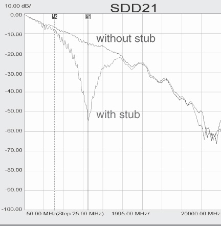
Figure 12-35 Measured differential return loss of two backplane channels, one with a 0.25-inch-long via stub and one with the via stub backdrilled. Measured with an Agilent N5230 VNA and displayed with Agilent’s PLTS. Data courtesy of Molex Corporation.
The sharp resonant dip at about 6 GHz is due to the quarter wave stub resonance and is a prime factor limiting the usable bandwidth of high-speed serial links.
The origin of the resonance is very easy to understand by referring to the illustration in Figure 12-36. In this illustration, the return path is not included but is present as planes on adjacent layers.
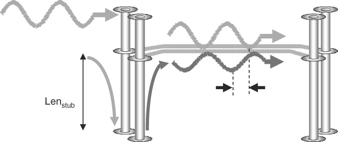
Figure 12-36 The insertion loss is due to the combination of the incident wave and reflected wave from the bottom of the via stub. When the stub length is one-quarter a wavelength, the two waves arriving at the receiver are 180 degrees out of phase and cancel out.
When the signal flows down the via to the connected signal layer, it splits. Part of the signal continues on the signal layer, and another part of the signal heads down to the end of the via stub, which is open.
When the signal hits the end of the via, it reflects and again splits at the layer transition. Some of the signal goes back to the source, while the rest of it continues in the same direction as the initial signal but with a phase shift.
The phase shift of the reflected wave is the round-trip path length going down to the stub and back up to the signal layer. When this round-trip path length is half a wave, the two components—the initial signal and the reflected signal—heading to port 2 will be 180 degrees out of phase and offer the most cancellation. The condition for maximum cancellation, the dip in the differential insertion loss, is that the round-trip time delay for the stub is half a cycle, or:
Or, for the case of Dk = 4:
Lenstub = length of the stub, in inches
v = speed of the signal, in inches/nsec
fres = resonant frequency for the stub, in GHz
Dk = dielectric constant of the laminate around the stub = 4
For example, if the stub is 0.25 inches long, the resonant frequency is 1.5 GHz/0.25 inches = 6 GHz, which is very close to what is observed.
The condition for maximum cancellation and the minimum differential insertion loss is that the round-trip length of a via stub be one-half a wavelength or that the one-way length be one-quarter of a wavelength. This is why this resonance is often called a quarter-wave stub resonance.
As a rough guideline, for the large resonant absorption in the stub to not affect the high-speed signal, the resonant frequency should be engineered to be a frequency that is at least twice the bandwidth of the signal. In the worst case, when the channel is low loss and short, the bandwidth of the signal would be roughly the fifth harmonic of the Nyquist. The Nyquist frequency is one-half the bit rate, so the signal bandwidth is:
where:
BW = bandwidth of the signal, in GHz
BR = bit rate, in Gbps
The condition for an acceptable via stub length is:
or:
where:
Lenstub = maximum acceptable stub length, in mils
BR = bit rate, in Gbps
TIP
For example, to engineer the stub resonant frequency to be far above the Nyquist frequency of a 5-Gbps signal so that no signal frequency components would see the resonant dip, the maximum length of any via stub in the channel should be shorter than 300/5 = 60 mils. This defines the design space for acceptable via stubs for 5-Gbps signals.
The via stub length can be engineered by restricting layer transitions between the top few layers and the bottom few layers, using thinner boards, backdrilling the long stubs, or using alternative via technologies such as blind and buried vias or microvias.
12.15 The Mode Conversion Terms
The off-diagonal quadrants of the differential S-parameter matrix are the most confusing, as they have information about how the differential pair interconnect converts differential signals into common signals and vice versa. They are also very important when it comes to hacking into the interconnect to determine possible root causes of behavior.
Even though it is incorrect to call the signal entering a port the differential mode signal, the industry has adopted a convention that is very confusing. These two off-diagonal quadrants are called the mode conversion quadrants, as they describe how one signal mode is converted into another signal mode.
The SCD quadrant describes how a differential signal enters the differential pair but comes out as a common signal. It can enter at one port and can come out that port or can be transmitted to the other port.
Only asymmetry between one line and the other line in a differential pair will convert some differential signal into common signal or vice versa. In a perfectly symmetrical differential pair, there is never any mode conversion. As long as what is done to one line is done to the other line, no matter how large the discontinuity, there will be no mode conversion, and the SCD terms will be zero.
Any asymmetry between the two lines that make up the differential pair will cause mode conversion. This can be a length difference, a local variation in the dielectric constant between the two lines, a test pad on one line but not the other, a difference in the rise time of the drivers, a skew between the drivers of the two channels, a variation in the clearance holes in a via field, or a line width difference. How much signal appears in the SCD11 term compared to the SCD21 term depends on how much common impedance discontinuity the common signal encounters to reflect some of the common signal back to the originating port.
The same asymmetry that converts a differential signal into a common signal will convert a common signal into a differential signal. Mode conversion creates three possible problems for differential pairs used in high-speed serial link applications.
The first problem is that if there is significant mode conversion of the differential signal, the differential signal amplitude can drop. This drop might increase the bit error rate. An example of the impact on the differential signal from a small length difference between the two lines in a differential pair is shown in Figure 12-37.
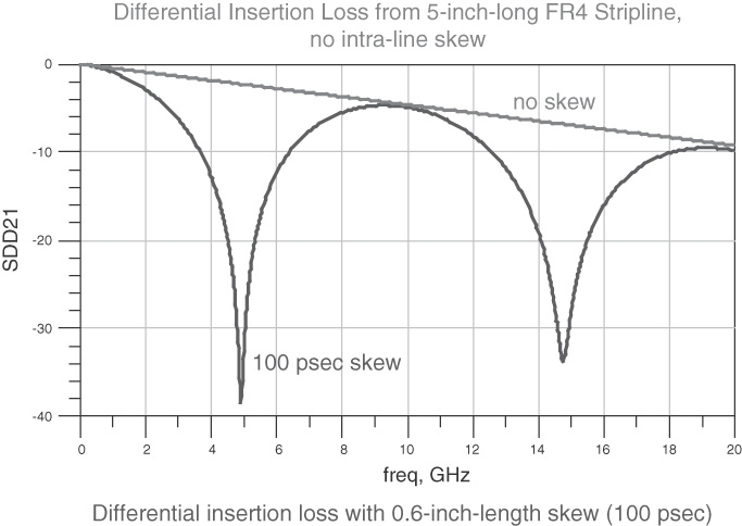
Figure 12-37 Differential insertion loss through a uniform differential pair, with no intra-line skew and with 100 psec of skew between the two lines. The skew causes a dip in the differential signal when the skew is one-half of a cycle. Simulated with Agilent’s ADS.
The second problem with mode conversion is that the common signal created might reflect from the unterminated ends of the differential pair, and each time it passes through the asymmetry, some of it might convert back into a differential signal, but asynchronous with the data stream, and distort the original differential signal. This would also increase the bit error rate by collapsing the eye.
The third problem with the common signal generated by mode conversion arises if the common signal gets out of the box and on an unshielded twisted-pair cable. A pure differential signal on a twisted-pair cable does not radiate EMI and has no problem passing an FCC or similar EMC certification test. However, if more than 3 microAmps of common signal at 100 MHz or higher frequency is created and gets out on 1 meter of twisted-pair cable, it will radiate and cause a failure in an FCC test.
If the common impedance is 300 Ohms, it takes only about 1 mV of common signal generated from mode conversion driving an unshielded, external twisted-pair cable to cause an FCC failure. Depending on the differential signal swing, this might be on the order of 1% mode conversion.
Figure 12-38 shows an example of the measured mode conversion in three different, differential channels routed adjacent to each other in a backplane. In each case, the converted common signal would exceed 1 mV. If any of this escaped onto external, unshielded twisted-pair cable, it could cause an FCC failure. However, if this common signal stays inside the box, it will not contribute to EMI. It may still cause a problem in distorting the differential signal, though.

Figure 12-38 Measured-mode conversion in the transmitted signal, SCD21, for three different channels in a backplane. The peak mode conversion is about −35 dB, which is slightly above 1%. If the differential signal were 100 mV, the common signal would be above 1 mV, and if this appeared on unshielded twisted pair, it would probably fail an FCC test. Measured with an Agilent N5230 VNA and displayed with Agilent’s PLTS.
12.16 Converting to Mixed-Mode S-Parameters
Virtually all instruments measure only the single-ended S-parameters. To display the mixed-mode S-parameters, the single-ended S-parameters are mathematically transformed into the mixed-mode S-parameters. For all linear, passive interconnects, the mixed-mode S-parameters are just a linear combination of the single-ended S-parameters.
Exactly how the 10 unique, single-ended S-parameters are transformed into the 10 unique differential S-parameters requires some complicated matrix math but is very straightforward to implement. The matrix math is summarized in a simple matrix equation:
Sd = mixed-mode or differential S-parameter matrix
M = transform matrix
Ss = single-ended S-parameter matrix that is typically measured
The transform matrix relates how single-ended matrix elements combine to create the mixed-mode matrix. When the port assignments are as described in this chapter, 1 → 2 and 3 → 4, the transform matrix is:

For example, the SDD11 element is given by:
and the SDD21 element is given by:
This matrix manipulation allows us to take any single-ended S-parameter matrix of measured or simulated S-parameters and routinely transform it into the differential or mixed-mode elements. This is another reason it is so important to use the correct port assignment because otherwise the transform matrix will change.
12.17 Time and Frequency Domains
For linear, passive interconnects, the same information contained in an individual S-parameter element can be displayed either in the frequency domain or in the time domain. After all, the frequency-domain S-parameters describe how any sine wave voltage waveform is treated by the interconnect. We can synthesize any time-domain waveform by combinations of different frequency components.
A linear system will have no interaction between the frequency components. If we know how each frequency component interacts with the interconnect, we can literally add up the right combinations of frequency components and evaluate any time-domain waveform. This is essentially the inverse Fourier transform process.
There are two commonly used synthesized time-domain waveforms that provide immediately useful information about an interconnect: a step edge and an impulse response. The reflected and transmitted behavior is interpreted slightly differently.
A step response is the same waveform used in a TDR and is often referred to as the TDR response. S11, when viewed in the time domain as a step response, is identical to a TDR response and has information about the single-ended impedance profile of an interconnect. The S21 term, when viewed in the time domain as a step edge, has information about how the leading or falling edge of a signal is distorted by the interconnect. This is usually dominated by losses in the interconnect.
When there are multiple responses to evaluate in the time domain, we usually use the S-parameter notation for each matrix element to signify which ports are involved, but instead of using the letter S, we use the letter T. For example, T11 is the TDR response, and T21 is the TDT response.
TIP
Each domain has the same information but displayed in a different format. They obviously look different visually, and each term has a different sensitivity to interconnect properties. Depending on the question being asked, one or the other format might be the right one to use to get to the answer faster.
For example, if the question is what is the characteristic impedance of the line, the T11 element would get us the answer the fastest. If the question is what are the losses in the line, the S21 element would get us the answer the fastest.
This is illustrated in Figure 12-39, where the same measured insertion and return loss of a line in a microstrip pair is displayed in the frequency and time domains. Included are examples of two microstrip lines: one in a tightly coupled pair and one in a weakly coupled pair.

Figure 12-39 Measured single-ended return and insertion loss for a single line in a microstrip pair. One pair is tightly coupled, and the other pair is loosely coupled. Exactly the same measured response is shown in the frequency domain and the time domain. Measured with an Agilent N5230 VNA and displayed with Agilent PLTS.
TIP
Even though the information content in the time domain and the frequency domain is exactly the same, the information that is immediately available from the front screen is different. To get to the answer the fastest, it is important to have flexibility in converting the S-parameters between the time and frequency domains and between single-ended and differential domains.
It is much easier to interpret the impedance profile of an interconnect from the step edge time-domain form of S11 than from the frequency-domain form. Likewise, the frequency-domain form of S21 is a more sensitive measure of the interconnect losses than the step time-domain response. Depending on the question being asked, one element in a particular domain might get you to the answer more quickly than another. This is why having flexibility in data mining all the S-parameters is valuable.
The impulse time-domain response is particularly useful when using the S-parameters as a behavioral model in circuit simulators or to emulate the interconnect’s response to any arbitrary waveform.
The impulse response is also sometimes called Green’s function of the interconnect. It describes how any tiny incident voltage is treated by the interconnect. If we know how the interconnect treats an impulse response, we can take any waveform in the time domain and describe it as a combination of successive impulse responses. Using a convolution integral, we can combine how each of the successive, scaled impulse responses is treated by the interconnect to get the output waveform.
This technique allows us to synthesize any arbitrary time-domain waveform, convolve it with the impulse response, and simulate the output waveform. One application is to emulate eye diagrams of interconnects, as diagrammed in Figure 12-40.

Figure 12-40 Process of simulating an eye diagram for an interconnect by convolving the impulse response with a synthesized pseudorandom bit sequence and overlaying each bit synchronously with the clock. Measured with an Agilent N5230 VNA and simulated and displayed with Agilent’s PLTS.
The SDD21 frequency-domain waveform is converted into the time-domain impulse-response waveform. A pseudorandom bit sequence (PRBS) is synthesized using an ideal square wave with some rise time. This time-domain waveform is convolved with the impulse response of the interconnect. Essentially, the impulse response says how each voltage point will be treated by the interconnect. The convolution integration takes each voltage point, multiplies it by the interconnect’s response, and adds up all the time-domain responses, walking along the time-domain waveform.
The result is how the interconnect would treat the synthesized waveform. It is the simulation of the output real-time waveform. This is an example of using the S-parameters as a behavioral model of the interconnect. Its measured performance in the frequency domain is used to simulate the expected performance in the time domain without knowing anything about the internal workings of the interconnect. Many commercially available tools do this simulation automatically.
The simulated real-time, differential responses from the single-ended measurements can be used to generate eye diagrams. The clock waveform is used to slice out one, two, or three consecutive bits, and all the bits in the real-time response are superimposed with infinite persistence. The resulting superposition of all possible bit signals looks like an eye and is called an eye diagram. Figure 12-41 shows an example of two eye diagrams for a 3.125-Gbps and a 6.25-Gbps serial signal as they would appear through the same backplane channel based on S-parameter measurements of the channel.

Figure 12-41 Emulated eye diagrams for a backplane channel at two different bit rates, based on the measured S-parameters. Measured with an Agilent N5230 VNA and simulated and displayed with Agilent’s PLTS.
Two important features of an eye diagram can often predict bit error rates: the vertical opening and the horizontal opening. The vertical opening is often called the collapse of the eye, and the horizontal opening is related to the bit period minus the deterministic jitter.
The center-to-center spacing of the crossovers is always the unit interval bit time. The width of the crossovers is a measure of the jitter. In the measured SDD21 response of an interconnect, the random jitter is related to the quality of the measurement instrument and is almost always negligible. All the jitter in a simulated eye diagram is deterministic in the sense that it is nonrandom and predictable from just the interconnect behavior. It arises from losses, impedance discontinuities, and other factors.
By synthesizing PRBS waveforms with different bit rates, a family of eye diagrams can be simulated to indicate the performance limits of an interconnect.
12.18 The Bottom Line
1. As a universal description of any interconnect, even though they are new to the signal-integrity field, S-parameters are quickly becoming an industry standard.
2. Each S-parameter is the ratio of an output sine wave to an input sine wave. It represents the behavior of the interconnect to sine waves across a defined frequency range.
3. The reflected S-parameters, S11 and S22, have information about impedance discontinuities of the interconnect.
4. The transmitted S-parameters, S21 and S43, have information about losses, discontinuities, and couplings to other lines.
5. Other terms may describe the cross talk between interconnects.
6. While the port impedance is generally 50 Ohms, the same S-parameter response can be transformed to any port impedance. If there is no compelling reason to use something else, 50 Ohms should always be used.
7. The single-ended S-parameters obtained in the frequency domain can be transformed into differential S-parameters or into the time domain.
8. S-parameters in the frequency domain are a measure of the overall integrated, steady-state response of the interconnect; while transformed in the time domain, S-parameters can provide spatial information about the properties of an interconnect.
9. Narrow dips in the return or insertion loss are indictors of coupling to high-Q resonating structures.
10. The differential insertion loss describes the most important property of a differential channel.
11. Mode conversion is described by two of the differential S-parameter matrix elements, SCD11 and SCD21. They are useful in debugging the root cause of drops in the insertion loss.
12. Everything you ever wanted to know about the behavior of an interconnect is contained in the S-parameters, obtained either through measurement or by simulation.
End-of-Chapter Review Questions
12.1 Fundamentally, what do S-parameters really measure?
12.2 What is another name for an S-parameter model of an interconnect structure?
12.3 In the frequency domain, what do S-parameters describe about the properties of an interconnect?
12.4 What is different about the S-parameter model of an interconnect when displayed in the time domain?
12.5 List four properties of an interconnect that could be data mined from their S-parameter model.
12.6 What is the significance of using a 50-Ohm port impedance?
12.7 Why is a there a factor of 20 instead of 10 when converting an S-parameter, as a fraction, into a dB value?
12.8 Which S-parameter term is the impedance of an interconnect most sensitive to?
12.9 Which S-parameter term is the attenuation in an interconnect most sensitive to?
12.10 What are the S-parameters of an ideal transparent interconnect?
12.11 What is the recommended port labeling scheme for a pair of transmission lines?
12.12 Which S-parameter term contains information about near-end cross talk between two transmission lines?
12.13 Which S-parameter term contains information about far-end cross talk between two transmission lines?
12.14 How many individual numbers are contained in the S-parameter model of a 4-port interconnect, measured from 10 MHz to 40 GHz at 10-MHz steps?
12.15 Using the historically correct definition of return loss, if the return loss increases, what happens to the reflection coefficient? Is this in the direction of a more transparent or less transparent interconnect?
12.16 Using the modern, conventional definition of insertion loss, if the insertion loss increases, what does the transmission coefficient do? Is this in the direction of a more or less transparent interconnect?
12.17 Suppose the reflection coefficient of a cable with 50-Ohm port impedances has a peak value of −35 dB. What would you estimate its characteristic impedance to be? Suppose the port impedance were changed to 75 Ohms. Would the peak reflection coefficient increase or decrease?
12.18 As two of the most important consistency tests for the S-parameter of a through interconnect, what should the return and insertion loss be at low frequency? How will this change if the impedance of the interconnect is increased?
12.19 What causes ripples in the reflection coefficient?
12.20 Above what magnitude of reflection coefficient will the return loss ripples begin to appear in the transmission coefficient?
12.21 Why does the phase of S21 increase in the negative direction?
12.22 Why does the polar plot of the S21 spiral inward with increasing frequency?
12.23 As a consistency test, what insertion loss would you expect for an FR4 interconnect at 10 GHz that is 20 inches long?
12.24 Why does S21 of one line in a microstrip show a deep dip at some frequency? What would be an important consistency test to test your explanation?
12.25 What is the most common source of sharp, narrow dips in the insertion loss of through connections?
12.26 What are the two types of signal that can appear on a differential pair?
12.27 What is the only feature that causes mode conversion in a differential pair? Which two S-parameter terms are strong indicators of mode conversion?
12.28 In an uncoupled differential pair, how would the differential insertion loss compare with the single-ended insertion loss of either line?
12.29 When displaying the TDR response of an interconnect, which S-parameter is displayed, and how do you interpret the display?
12.30 What information will be in the TDT response of a through interconnect?