
5
Design Options for Basic Building Blocks
5.1 Introduction
A detailed description of system-level design of signal processing algorithms and their representation as dataflow graphs (DFGs) is given in Chapter 4. A natural sequel is to discuss design options for the fundamental operations that are the building blocks for hardware mapping of an algorithm. These blocks constitute the data path of the design that primarily implements the number-crunching. They perform addition, subtraction, multiplication and arithmetic and logic shifts.
This chapter covers design options for parallel adders, multipliers and barrel shifters. Almost all vendors of field-programmable gate arrays (FPGAs) are now also embedding hundreds of basic building blocks. The incorporation of fast adders and multipliers along with hard and soft micros of microcontrollers has given a new dimension to the subject of digital design. The hardware can run in close proximity to the software running on embedded processors. The hardware can be designed either as an extension to the instruction set or as an accelerator to execute computationally intensive parts of the application while the code-intensive part executes on the embedded processor.
This trend of embedding basic computational units on an FPGA has also encouraged designers to think at a higher level of abstraction while mapping signal processing algorithms in HW. There are still instances where a designer may find it more optimal to explore all the design options to further optimize the design by exercising the architecture alternatives of the basic building blocks. This chapter gives a detailed account of using these already embedded building blocks in the design. The chapter then describes architectural design options for basic computational blocks.
5.2 Embedded Processors and Arithmetic Units in FPGAs
FPGAs have emerged as exciting devices for mapping high-throughput signal processing applications. For these applications the FPGAs outperform their traditional competing technology of digital signal processors (DSPs). No matter how many MACs the DSP vendor can place on a chip, still it cannot compete with the availability of hundreds of these units on a high-end FPGA device. The modern day FPGAs come with embedded processors, standard interfaces and signal processing building blocks consisting of multipliers, adders, registers and multiplexers. Different devices in a family come with varying numbers of these embedded units, and it is expected that the number and type of these building blocks on FPGAs will see an upward trend.
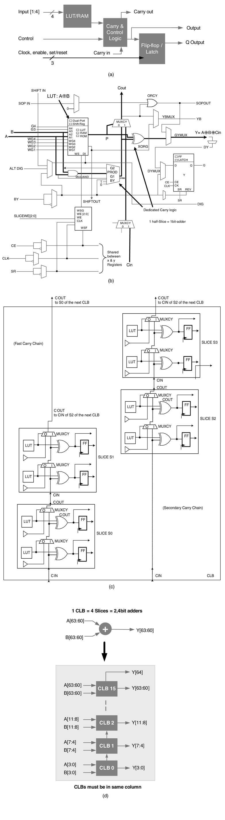
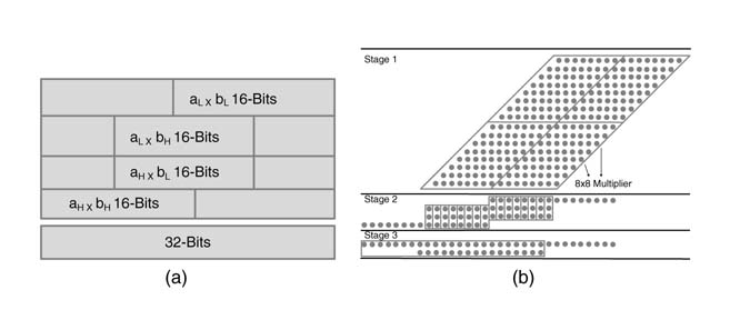
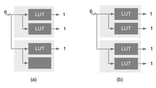
For example, the Xilinx Virtex™-4 and Virtex™-5 devices come with DSP48 and DSP48e blocks, respectively [1,2]. The DSP48 block has one 18 × 18-bit two’s complement multiplier followed by three 48-bit multiplexers, one 3-input 48-bit adder/subtractor and a number of registers. This block is shown in Figure 5.1(a). The registers in the block can be effectively used to add pipeline stages to the multiplier and adder. Each DSP48 block is independently configurable and has 40 different modes of operation. These modes are dynamically reconfigurable and can be changed in every clock cycle.
Similarly the Virtex™-II, Virtex™-II Pro, Spartan™ 3 and Spartan™ 3E devices are embedded with a number of two’s complement 18 × 18-bit multipliers as shown in Figure 5.1(d). Figure 5.1(b) and Figure 5.1(c) show arithmetic blocks in Altera and QuickLogic FPGAs.
Figure 5.1 Dedicated computational blocks. (a) DSP48 in Virtex™-4 FPGA (derived from Xilinx documentation). (b) 18 × 18 multiplier and adder in Altera FPGA. (c)8 × 8 multiplier and 16-bit adder in Quick Logic FPGA. (d) 18 × 18 multiplier in Virtex-II, Virtex-II pro and Spartan™-3 FPGA
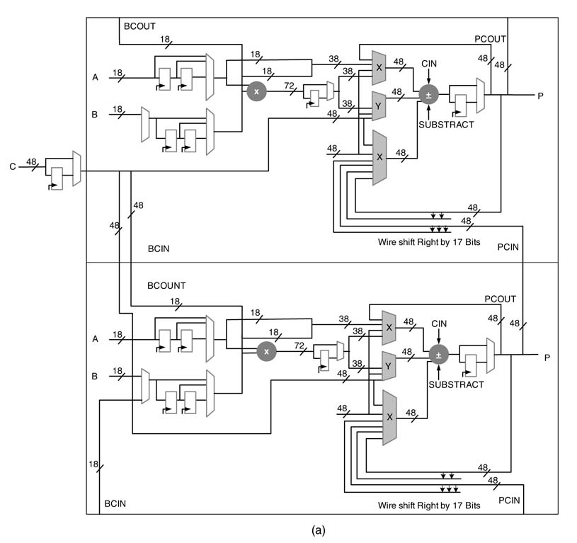
Figure 5.2 FPGA with PowerPC, MicroBlaze, Ethernet MAC and other embedded interfaces
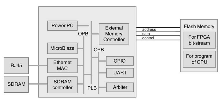
The FPGA vendors are also incorporating cores of programmable processors and numerous high speed interfaces. High-end devices in Xilinx FPGAs are embedded with Hard IP core of PowerPC or Soft IP core of Microblaze, along with standard interfaces like PCI Express and Gigabit Ethernet. A representative configuration of a Xilinx FPGA is shown in Figure 5.2. Similarly the Altera FPGA offers ARM Soft IP cores.
As this chapter deals with basic building blocks, it focuses primarily on embedded blocks and their use in hardware design. Most of the available synthesis tools automatically instantiate the relevant embedded blocks while synthesizing HDL (hardware description language) code that contains related mathematical operators.
The user may need to set synthesis options for directing the tool to automatically use these components in the design. For example, in the Xilinx integrated software environment (ISE) there is an option in the synthesis menu to select auto or manual use of the basic building blocks. In cases where higher order operations are used in the register transfer level (RTL) code, the tool puts multiple copies of these blocks together to get the desired functionality. For example, if the design requires a 32 x 32-bit multiplier, the synthesis tool puts four 18x18 multipliers to infer the desired functionality.
The user can also make an explicit instantiation to one of these blocks if required. For the target devices, the templates for such instantiation are provided by the vendors. Once the tool finds out that the device has run out of embedded HW resources of multipliers and adders, it then generates these building blocks using generic logic components on these devices. These generated blocks obviously perform less efficiently than the embedded blocks. The embedded resources indeed improve performance of an implementation by a quantum.
5.3 Instantiation of Embedded Blocks
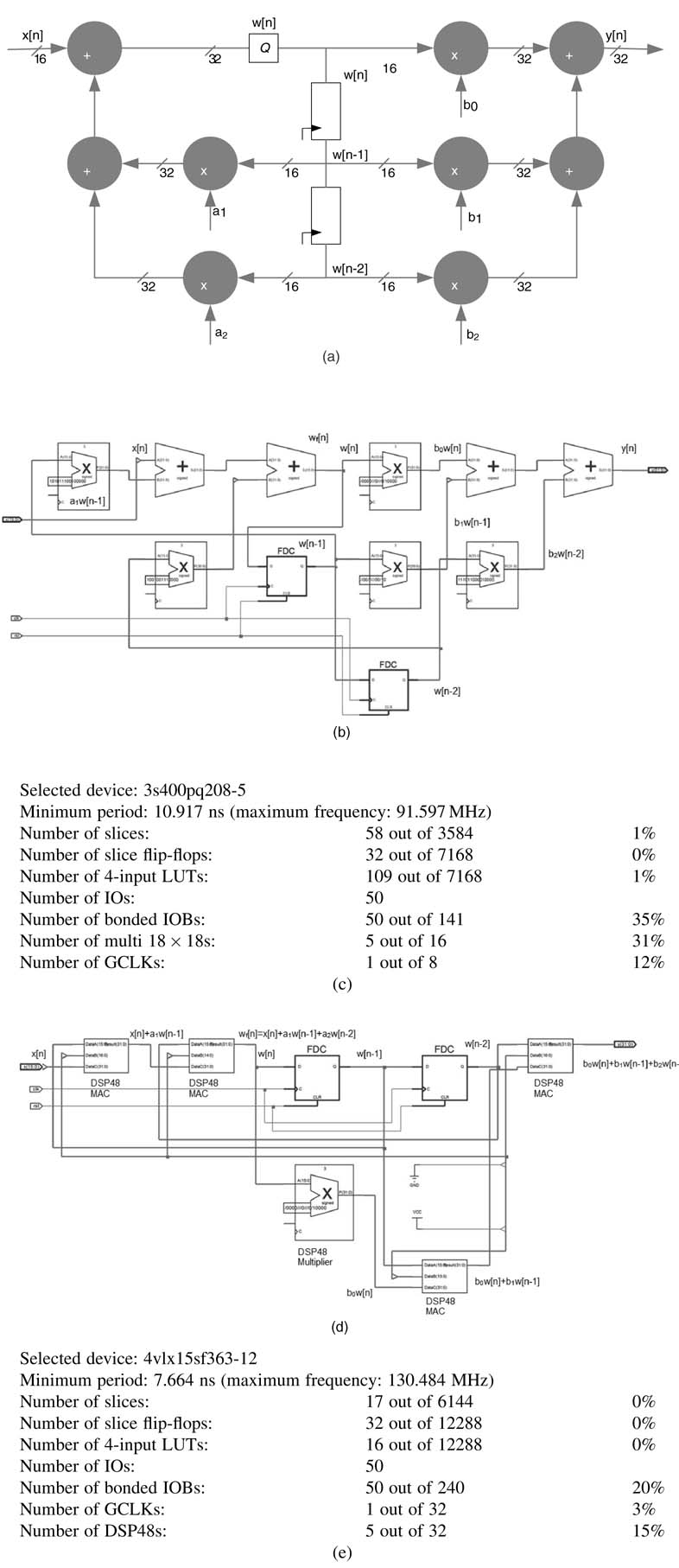
To demonstrate the effectiveness of embedded blocks in HW design, an example codes a second-order infinite impulse response (IIR) filter in Direct Form (DF)-II realization. The block diagram of
Figure 5.3 Hardware implementation of a second-order IIR filter on FPGA. (a) Block diagram of a second-order IIR filter in Direct Form-II realization. (b) RTL schematic generated by Xilinx’s Integrated Software Environment (ISE). Each multiplication operation is mapped on an embedded 18x18 multiplier block of Xiliinx Spartan™ 3 FPGA. (c) Synthesis summary report of the design on Spartan™-3 FPGA. (d) RTL schematic generated by Xilinx ISE for Virtex™ 4 target device. The multiplication and addition operations are mapped on DSP48 multiply accumulate (MAC) embedded blocks. (e) Synthesis summary report for the RTL schematic of (d)
the filter is shown in Figure 5.3, to implement the difference equations:
RTL Verilog code of a fixed-point implementation of the design is listed here:
module iir(xn, clk, rst, yn);
// x[n] is in Q1.15 format
input signed [15:0] xn;
input clk, rst;
output reg signed [31:0] yn; // y[n] is in Q2.30 format
wire signed [31:0] wfn; // Full precision w[n] in Q2.30 format
wire signed [15:0] wn; // Quantized w[n] in Q1.15 format
reg signed [15:0] wn_1, wn_2; // w[N -1]and w[N -2] in Q1.15 format
// all the coefficients are in Q1.15 format
wire signed [15:0] b0 = 16’h0008;
wire signed [15:0] b1=16’h0010;
wire signed [15:0] b2 = 16’h0008;
wire signed [15:0] a1=16’h8000;
wire signed [15:0] a2 = 16’h7a70;
assign wfn = wn_1*a1+wn_2*a2; // w[n] inQ2.30 format with one redundant
 sign bit
/* through away redundant sign bit and keeping
 16 MSB and adding x[n] to get w[n] in Q1.15 format */
assign wn = wfn[30:16]+xn;
//assign yn = b0*wn + b1*wn_1 + b2*wn_2; // computing y[n] inQ2.30 format
 with one redundant sign bit
always @(posedge clk or posedge rst)
begin
 if(rst)
 begin
 wn_1 <= #10;
 wn_2 <= #10;
 yn <= #10;
 end
 else
 begin
 wn_1 <= #1 wn;
 wn_2 <= #1 wn_1;
 yn <= #1 b0*wn + b1*wn_1 + b2*wn_2; // computing y[n] in Q2.30
 format with one redundant
 sign bit
 end
 end
end module
The design assumes that x[n] and all the coefficients of the filter are in Q1.15 format. To demonstrate the usability of embedded blocks on FPGA, the code is synthesized for one of the Spartan™-3 family of devices. These devices come with embedded 18x18 multiplier blocks. In the synthesis option, the Xilinx ISE tool is directed to use the embedded multiplier blocks. The post-synthesis report shows the design is realized using five MULT 18x18 blocks. As there is no embedded adder in the Spartan™-3 family of devices, the tool creates a 32-bit adder using the fast carry chain logic provided in the LUT. A summary of the synthesis report listed in Figure 5.3(c) and schematic diagram given in (b) provide details of the Spartan™-3 resources being used by the design.
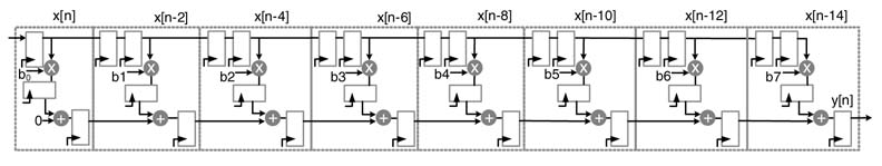
Figure 5.4 An 8-tap direct form (DF-I) FIR filter
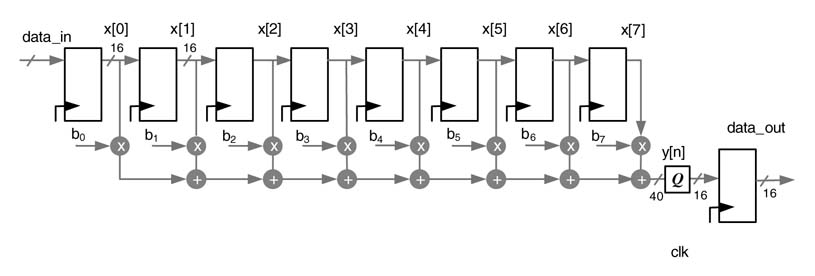
To observe the effectiveness of DSP48 blocks in Virtex™-4 FPGAs, the design is synthesized again after changing the device selection. As the tool is still directed to use DSP48 blocks, the synthesis result shows the use of five DSP48 blocks in the design, as is obvious from Figures Figure 5.3(d) and Figure 5.3(e) showing the schematic and a summary of the synthesis report of the design. Both the schematic diagrams are labeled with the actual variables and operators to demonstrate their relevance with the original block diagram. Virtex™-4 is clearly a superior technology and gives better timing for the same design. It is pertinent to point out that the synthesis timings given in this chapter are post-synthesis; although they give a good estimate, the true timings come after placement and routing of the design.
5.3.1 Example of Optimized Mapping
The Spartan™-3 family of FPGAs embeds dedicated 18 × 18-bit two’s complement multipliers to speed up computation. The family offers different numbers of multipliers ranging from 4 to 104 in a single device. These dedicated multipliers help in fast and power-efficient implementation of DSP algorithms. Here a simple example illustrates the simplicity of embedding dedicated blocks in a design. The 8-tap FIR filter of Figure 5.4 is implemented in Verilog. The RTL code is listed below:
// Module: fir_filter
// Discrete-Time FIR Filter
// Filter Structure: Direct-Form FIR
// Filter Order: 7
// Input Format: Q1.15
// Output Format: Q1.15
module fir_filter (
input clk,
input signed [15:0] data_in, //Q1.15
output reg signed [15:0] data_out //Q1.15
);
// Constants, filter is designed using Matlab FDATool, all coefficients are in
// Q1.15 format
parameter signed [15:0] b0 = 16’b1101110110111011;
parameter signed [15:0] b1 = 16’b1110101010001110;
parameter signed [15:0] b2 = 16’b0011001111011011;
parameter signed [15:0] b3 = 16’b0110100000001000;
parameter signed [15:0] b4 = 16’b0110100000001000;
parameter signed [15:0] b5 = 16’b0011001111011011;
parameter signed [15:0] b6 = 16’b1110101010001110;
parameter signed [15:0] b7 = 16’b1101110110111011;
reg signed [15:0] xn [0:7]; // input sample delay line
wire signed [39:0] yn; //Q8.32
// Block Statements
 always @(posedge clk)
 begin
 xn[0] <= data_in;
 xn[1] <= xn[0];
 xn[2] <= xn[1];
 xn[3] <= xn[2];
 xn[4] <= xn[3];
 xn[5] <= xn[4];
 xn[6] <= xn[5];
 xn[7] <= xn[6];
 data_out <= yn[30:15]; // bring the output back in Q1.15
 //format
 end
 assign yn = xn[0] *b0+xn[1] *b1+xn[2] *b2+xn[3] *b3 + xn[4] * b4 + xn[5] *b5+xn[6] *b6 + xn[7] *b7;
end module
The tool automatically infers eight of the embedded 18 × 18-bit multipliers. The synthesis report of Table 5.1(a) and schematic of Figure 5.5 clearly show the use of embedded multipliers in the design. The developer can also use an explicit instantiation of the multiplier by appropriately selecting the correct instance in the Device Primitive Instantiation option of the Language Template icon
Table 5.1 Synthesis reports: (a) Eight 18 × 18-bit embedded multipliers and seven adders from generic logic blocks are used on a Spartan™-3 family of FPGA. (b) Eight DSP48 embedded blocks are used once mapped on a Vertix™-4 family of FPGA
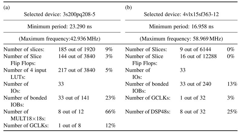
Figure 5.5 Schematic displaying the use of eight 18x18 embedded multiplier of Spartan™-3 FPGA provided in the ISE toolbar. The code for the instance from the ISE-provided template is given here:
// MULT18X18: 18x18 signed asynchronous multiplier
// Virtex™-II/II-Pro, Spartan™-3
// Xilinx HDL Language Template, version 9.1i
MULT18X18 MULT18X18_inst (
 .P(P), // 36-bit multiplier output
 .A(A), // 18-bit multiplier input
 .B(B) // 18-bit multiplier input
);
// End of MULT18X18_inst instantiation
As there is no embedded adder in the Spartan™-3 family of FPGAs, the tool crafts an adder using general-purpose logic. If in the device options we select a device in the Vierter™-4 family of FPGAs, which has several DSP48 blocks, then the tool uses MACs in the design and that obviously outperforms the Spartan™ design. The synthesis report of this design option is given in Table 5.1(b).
5.3.2 Design Optimization for the Target Technology
Although a digital design and its subsequent RTL Verilog implementation should be independent of technology, in many cases it is imperative to understand the target technology - especially when the device embeds dedicated arithmetic blocks. A design can effectively use the dedicated resources to their full potential and can improve performance many-fold without any additional HW cost.
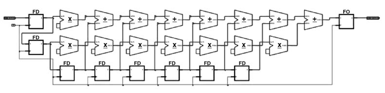
To substantiate this statement, the FIR filter implementation of Figure 5.4 is redesigned for optimized mapping on devices with embedded DSP48 blocks. The objective is to use the potential of the DSP48 blocks. Each can add two stages of pipelining in the MAC operation. If the code does not require any pipelining in the MAC operation, these registers are bypassed. The design in Figure 5.4 works without pipelining the MAC and registers in the DSP48 blocks are not used. A pipeline implementation for FIR filter is shown in Figure 5.6. This effectively uses the pipeline registers in the embedded blocks. The RTL Verilog code is listed below:
Figure 5.6 Pipeline implementation of 8-tap FIR filter optimized for mapping on FPGAs with DSP48 embedded blocks
module fir_filter_pipeline (
 input clk;
 input signed [15:0] data_in; //Q1.15
 output signed [15:0] data_out; //Q1.15
// Constants, filter is designed using Matlab FDATool, all coefficients are in
//Q1.15 format
parameter signed [15:0] b0 = 16’b1101110110111011;
parameter signed [15:0] b1 = 16’b1110101010001110;
parameter signed [15:0] b2 = 16b0011001111011011;
parameter signed [15:0] b3 = 16b0110100000001000;
parameter signed [15:0] b4 = 16b0110100000001000;
parameter signed [15:0] b5 = 16b0011001111011011;
parameter signed [15:0] b6 = 16b1110101010001110;
parameter signed [15:0] b7 = 16b1101110110111011;
reg signed [15:0] xn [0:14]; //one stage pipelined input sample delay line
reg signed [32:0] prod [0:7]; // pipeline product registers in Q2.30 format
wire signed [39:0] yn; //Q10.30
reg signed [39:0] mac [0:7]; // pipelined MAC registers in Q10.30 format
integer i;
always @(posedge clk)
begin
xn[0] <= data_in;
for (i=0; i<14; i=i+1)
xn[i+1] = xn[i];
data_out <= yn[30:15]; //bring the output back in Q1.15 format
end
always @(posedge clk)
begin
prod[0] <=xn[0] *b0;
prod[1] <=xn[2] *b1;
prod[2] <=xn[4] *b2;
prod[3] <=xn[6] *b3;
prod[4] <=xn[8] *b4;
prod[5] <=xn[10] * b5;
prod[6] <=xn[12] * b6;
prod[7] <=xn[14] *b7;
end
always @(posedge clk)
begin
mac[0] <=prod[0];
for (i=0; i<7; i=i+1)
mac[i+1] <= mac[i]+prod[i+1];
end
assign yn = mac[7];
end module
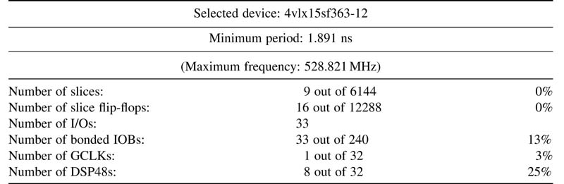
The design is synthesized and the synthesis report in Table 5.2 reveals that, athough the design uses exactly the same amount of resources, it results in a ~9-fold improvement in timing. This design can run at 528.82 MHz, compared to its DF-I counterpart that compiles for 58.96 MHz of best timing.
Table 5.2 Synthesis report of mapping pipelined 8-tap FIR filter on Virtex™-4 family of FPGA
It is important to point out that the timing for the DF-I realization increases linearly with the length of the filter, whereas the timing for the pipeline implementation is independent of the length of the filter.
Several other effective techniques and structures for implementing FIR filters are covered in Chapter 6.
5.4 Basic Building Blocks: Introduction
After the foregoing discussion of the use of dedicated multipliers and MAC blocks, it is pertinent to look at the architectures for the basic building blocks. This should help the designer to appreciate the different options for some of the very basic mathematical operations, and elucidate the tradeoffs in the design space exploration. This should encourage the reader to always explore design alternatives, no matter how simple the design. It is also important to understand that a designer should always prefer to use the dedicated blocks.
Several architectural options are available for selecting an appropriate HW block for operations like addition, multiplication and shifting. The following sections discuss some of these design options.
5.5 Adders
5.5.1 Overview
Adders are used in addition, subtraction, multiplication and division. The speed of any digital design of a signal processing or communication system depends heavily on these functional units. The ripple carry adder (RCA) is the slowest in adder family. It implements the traditional way of adding numbers, where two bits and a carry of addition from the previous bit position are added and a sum and a carry-out is computed. This carry is propagated to the next bit position for sequential addition of the rest of the significant bits in the numbers. Although the carry propagation makes it the slowest adder, its simplicity gives it the minimum gate count.
To cater for the slow carry propagation, fast adders are designed. These make the process of carry generation and its propagation faster. For example, in a carry look-ahead adder the carry-in for all the bit positions are generated simultaneously by a carry look-ahead generator logic [3, 4].This helps in the computation of a sum in parallel with the generation of carries without waiting for their propagation. This results in a constant addition time independent of the length of the adder. As the word length increases, the hardware organization of the carry generation logic gets complicated. Hence adders with a large number of elements are implemented in two or three levels of carry look-ahead stages.
Another fast devive is the carry select adder (CSA) [5]. This partitions the addition in K groups; to gain speed the logic is replicated and for each group addition is performed assuming carry-in 0 and 1. The correct sum and carry-out from each group is selected by carry-out from the previous group. The selected carry-out is used to select sum and carry-out of the next adjacent group. For adding large numbers a hierarchical CSA is used; this divides the addition into multiple levels.
A conditional sum adder can be regarded as a CSA with maximum possible levels. The carry select operation in the first level is performed on 1-bit groups. In the next level two adjacent groups are merged to give the result of a 2-bit carry select operation. Merging of two adjacent groups is repeated until the last two groups are merged to generate the final sum and carry-out. The conditional sum adder is the fastest in adder family [6]. It is a log-time adder and the size of the adder can be doubled by the addition of one 2:1 multiplexer delay.
This chapter presents architectural details and lists RTL Verilog code for a few designs. It is importanttohighlightthatmappinganadderonanFPGAmaynotyieldexpectedperformanceresults. This is due primarily to the fact that FPGAs are embedded with blocks that favor certain designs over others. For example, a fast carry chain in many FPGA families of devices greatly helps an RCA; soon these FPGAs, an RCA to a certain bit width is the best design option for area and time.
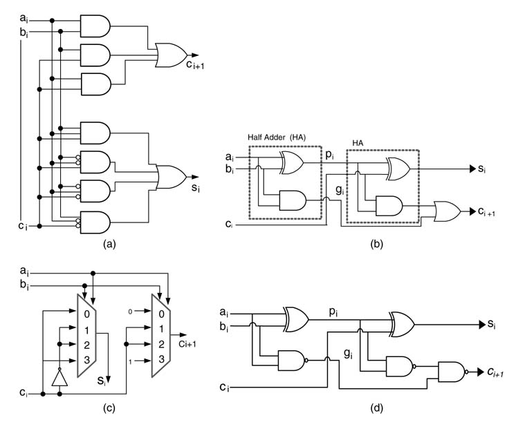
5.5.2 Half Adders and Full Adders
A half adder (HA) is a combinational circuit used for adding two bits, ai and bi , without a carry-in. The sum si and carry output ci are given by:
The critical path delay is one gate delay, and it corresponds to the length of any one of the two paths.
A full adder (FA) adds three bits. A 3-bit adder is also called a 3:2 compressor. One way to implement a full adder is to use the following equations:
There are several gate-level designs to implement a full adder, some of which are shown in Figure 5.7. These options to implement a simple mathematical operation of adding three bits also emphasize our initial assertion that the designer must avoid gate-level modeling and dataflow modeling using bitwise operators. It is not possible for an RTL designer to know the optimal design without knowing the target libraries. In many instances it is preferred that the design should be at RTL and is technology-independent. In design instances where the target technology is known a priori , then the designer can craft an optimal design by effectively using the optimized components from the technology library. The earlier example of Section 5.3.2 provides a better comprehension of this design rule where DSP48 blocks in the Virtex™-4 family of devices are effectively used to gain a nine times better performance without adding any additional resources compared to a technology-independent RTL implementation.
Figure 5.7 Gate-level design options for a full adder
5.5.3 Ripple Carry Adder
The emphasis of this text is on high-speed architecture, and an RCA is perceived to be the slowest adder. This perception can be proven wrong if the design is mapped on an FPGA with embedded carry chain logic. An RCA takes minimum area and exhibits a regular structure. The structure is very desirable especially in the case of an FPGA mapping as the adders fit easily into a 2-dimensional layout. An RCA can also be pipelined for improved speed.
A ripple adder that adds two N -bit operands requires N full adders. The speed varies linearly with the word length. The RCA implements the conventional way of adding two numbers. In this architecture the operands are added bitwise from the least significant bits (LSBs) to the most significant (MSBs), adding at each stage the carry from the previous stage. Thus the carry-out from the FA at stage i goes into the FA at stage (i +1), and in this manner carry ripples from LSB to MSB (hence the name of ripple carry adder):
Figure 5.8 A 6-bit ripple carry adder
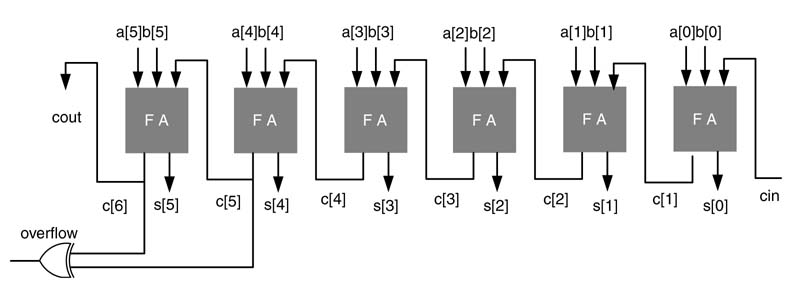
A 6-bit RCA is shown in Figure 5.8. The overflow condition is easily computed by simply performing an XOR operation on the carry-out from the last two full adders. This overflow computation is also depicted in the figure.
The critical path delay of a ripple carry adder is:
where TRCA is the delay of an N -bit ripple carry adder, while TFA and Tm are delays of an FA and the carry generation logic of the FA, respectively.
It is evident from (5.5) that the performance of an RCA is constrained by the rippling of carries from the first FA to the last. To speed the propagation of the carry, most FPGAs are supported with fast carry propagation and sum generation logic. The carry propagation logic provides fast paths for the carry to go from one block to another. This helps the designer to implement fast RCA on the FPGA. The user can still implement parallel adders discussed in this chapter, but their mapping on FGPA logic may not generate adequate speed-ups as expected by the user when compared with the simplest RCA performance. In many design instances the designer may find an RCA as the fastest adder compared to other parallel adders discussed here.
Verilog implementation of a 16-bit RCA through dataflow modeling is given below. This implementation, besides using registers for input and output signals, simply uses addition operators, and most synthesis tools will (if not directed otherwise) infer an RCA from this statement:
module ripple_carry_adder #(parameter W=16)
( input clk,
 input [W-1:0] a, b,
 input cin,
 output reg [W-1:0] s_r,
 output reg cout_r);
wire [W-1:0] s;
wire cout;
reg [W-1:0] a_r, b_r;
reg c in_r;
assign {coot’s} = a_r + b_r + c in_r;
always@(posedge clk)
begin
 a_r<=a;
 b_r<=b;
 c in_r<=cin;
 s_r<=s;
cout_r<= cout;
 end
end module
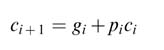
If the code is synthesized for an FPGA that supports fast carry chain logic, like Vertix™-II pro, then the synthesis tool will infer this logic for fast propagation of the carry signal across the adder.
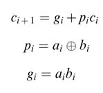
A Vertix™-II pro FPGA consists of a number of configurable logic blocks (CLBs), and each CLB has four ‘slices’. Each slice further has two look-up tables (LUTs) and dedicated logic to compute generate (g) and propagate (p ) functions. These functions are used by the synthesis tool to infer carry logic for implementing a fast RCA. The equations of gi and pi and logic it uses for generating fast carry-out c i+1 in a chain across an RCA are:
This is shown in Figure 5.9(a) and Figure 5.9(b). When the Verilog code of this section is synthesized on the device, the synthesized design uses fast carry logic in cascade to tie four CLBs in a column to implement a 16-bit RCA. The logic of 16-bit and 64-bit adders is shown in Figure 5.10(c) and Figure 5.10(d), respectively.
5.5.4 Fast Adders
If not mapped on an FPGA with fast carry chain logic, an RCA usually is the slowest adder as each full adder requires carry-out from the previous one for its sum and carry-out computation. Several alternative architectures have been pro This design can be easily pipelined by placing registers after any number of multiplexers and appropriately delaying the respective selection bit for coherent operation. A fully pipelined design of a barrel shifter is given in Figure 5.23(b), and the code for RTLVerilog implementation of the design is listed here:posed in the literature. All these architectures somehow accelerate the generation of carries for each stage. This acceleration results in additional logic. For FGPA implementation the designer needs to carefully select a fast adder because some have carry acceleration techniques well suited for FPGA architectures while others do not. As already discussed, an RCA makes the most optimal use of carry chains, although all the full adders need to fit in a column for effective use of this logic. This usually is easily achieved. ACSA also replicates RCA blocks, so each block still makes an effective use of fast carry chain logic with some additional logic for the selection of one sum out of two sums computed in parallel.
5.5.5 Carry Look-ahead Adder
A closer inspection of the carry generation process reveals that a carry does not have to depend explicitly on the preceding carries. In a carry look-ahead adder the carries entering all the bit positions of the adder are generated simultaneously by a carry look-ahead (CLA) generator; that is, computation of carries takes place in parallel with sum calculation. This results in a constant addition time independent of the length of the adder. As the word length increases, the hardware organization of the addition technique gets complicated. Hence adders with a large number of elements may require two or three levels of carry look-ahead stages.
Figure 5.9 (a) Fast-carry logic blocks. (b) Fast-carry logic in Vertix™-II pro FPGA slice. (c) One CLB of Vertix™-II pro inferring two 4-bit adders, thus requiring four CLBs to implement a 16-bit adder. (d) A 64-bit RCA using fast-carry chain logic (derived from Xilinx documentation)
A simple consideration of full adder logic identifies that a carry c i+1 is generated if ai =bi =1, and a carry is propagated if either ai or bi is 1. This can be written as:
Thus a given stage generates a carry if gi is TRUE and propagates a carry-into the next stage if pi is TRUE. Using these relationships, the carries can be generated in parallel as:
Figure 5.10 CLA logic for computing carries in two-gate delay time
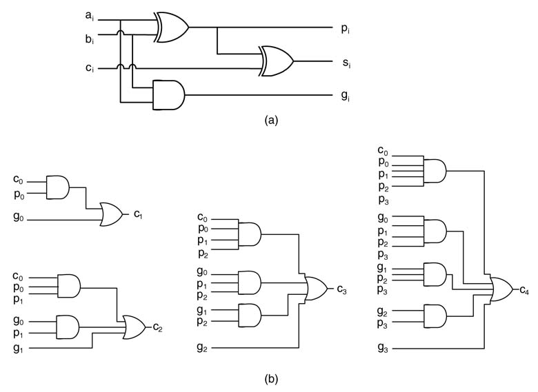
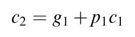
Figure 5.10 shows that all carries can be computed in a time of two gate delays. The block in carry look-ahead architecture can be of any size, but the number of inputs to the logic gates increases with the size. In closed form, we can write the carry at position i as:
This requires i + 1 gates with a faN -in of i +1. Thus each additional position will increase the faN -in of the logic gates.
Industrial practice is to use 4-bit wide blocks. This limits the computation of carries until c3, and c4 is not computed. The first four terms in c4 are grouped as G0 and the product p 3p 2p 1p 0 in the last term is tagged as P0 as given here:
Let:
Now the group G0 and P0 are used in the second level of the CLA to produce c4 as:
Similarly, bits 4 to7are also grouped together and c5 ,c6 and c7 are computed in the first level of the CLA block using c4 from the second level of CLA logic. The first-level CLA block for these bits also generates G1 and P1 .
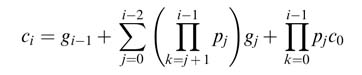
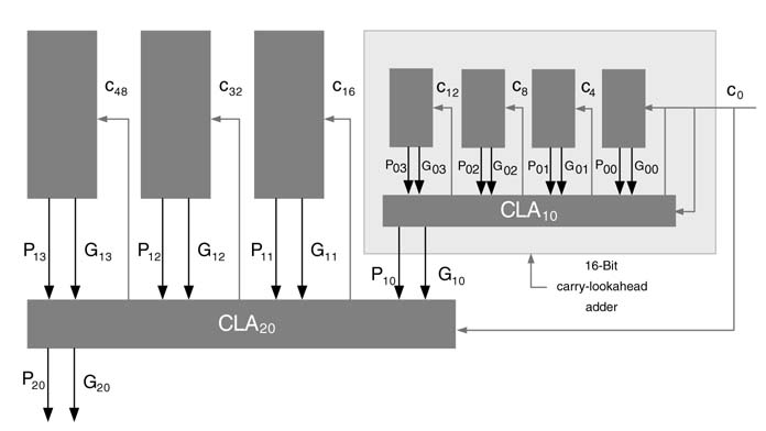
Figure 5.11 shows a 16-bit adder using four carry look-ahead 4-bit wide blocks in the first level. Each block also computes its G and P using the same CLA as used in the first level. Thus the second level generates all the carries c 4, c 8 and c 12 required by the first-level CLAs. In this way the design is hierarchically broken down for efficient implementation. The same strategy is further extended to build higher order adders. Figure 5.12 shows a 64-bit carry look-ahead adder using three levels of CLA logic hierarchy.
5.5.6 Hybrid Ripple Carry and Carry Look-ahead Adder
Instead of hierarchically building a larger carry look-ahead adder using multiple levels of CLA logic, the carry can simply be rippled between blocks. This hybrid adder is a good compromise as it yields an adder that is faster than RCA and takes less area than a hierarchical carry look-ahead adder. A 12-bit hybrid ripple carry and carry look-ahead adder is shown in Figure 5.13.
5.5.7 Binary Carry Look-ahead Adder
The BCLA works in a group of two adjacent bits, and then from LSB to MSB successively combines two groups to formulate a new group and its corresponding carry. The logic for the carry generation of an N -bit adder is:
The problem can be solved recursively as:
for i = 1 to N – 1
end
Figure 5.11 A 16-bit carry look-ahead adder using two levels of CLA logic
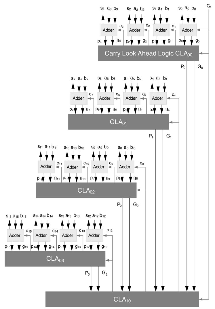
Figure 5.12 A 64-bit carry look-ahead adder using three levels of CLA logic
where the dot operator · is given as:
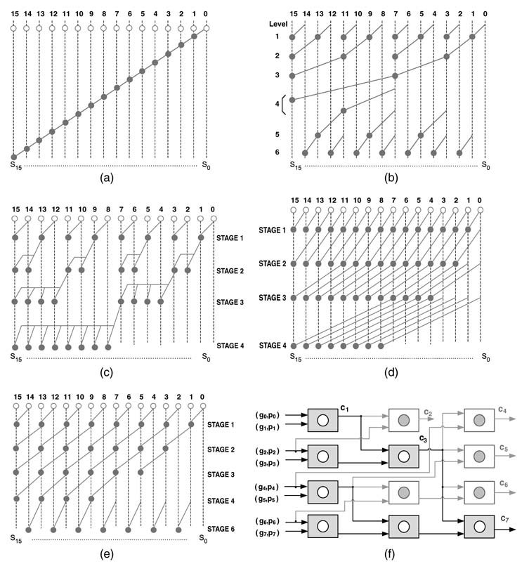
There are several ways to logarithmically break the recursion into stages. The objective is to implement (5.9) for each bit position. Moving from LSB to MSB, this requires successive application of the · operator on two adjacent bit positions. For an N -bit adder, a serial implementation will require N – 1 stages of operator implementation, as shown in Figure 5.14(a). Several optimized implementations are reported in the literature that improve on the serial realization [7, 8]. These are shown in Figure 5.14(b)-Figure 5.14(e). That in (b) is referred to as a Brent-Kung Adder and results in a regular layout, shown in (f) where the tree depicted in black color is forward tree and calculates carry-out to the adder in minimum time. The RTL Verilog code and stimulus of a 16-bit linear BCLA is given here:
module Binary Carry Look a head Adder
# (parameter N = 16)(
input [N -1:0] a,b,
input c_in,
output reg [N -1:0] sum,
output reg c_out);
reg [N -1:0] p, g, P, G;
reg [N:0] c;
integer i;

always@(*)
 begin
 for (i=0;i<N;i=i+1)
 begin
 // Generate all ps and gs
 p[i]= a[i] ^ b[i];
 g[i]=a[i] & b[i];
 end
 end
Figure 5.13 A 12-bit hybrid ripple carry and carry look-ahead adder
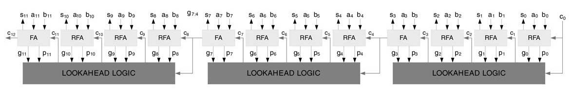
Figure 5.14 Binary carry look-ahead adder logic for generating all the carries in a tree of logic moving from LSB to MSB. (a) Serial implementation. (b) Brent–Kung adder. (c) Ladner–Fischer parallel prefix adder. (d) Kogge–Stone parallel prefix adder. (e) Han–Carlson parallel prefix adder. (f) Regular layout of an 8-bit Brent–Kung adder
always@(*)
begin
 // Linearly apply dot operators
 P[0] = p[0];
 G[0] = g[0];
 for (i=1; i<N; i=i+1)
 begin
 P[i]= p[i] &
 P[i-1]; G[i]= g[i] | (p[i] & G[i-1]);
 end
end
always@(*)
begin
 //Generate all carries and sum
 c[0]=c_in;
 for(i=0;i<N;i=i+1)
 begin
 c[i+1] = G[i] | (P[i] & c[0]);
 sum[i] = p[i] ^ c[i];
 end
 c_out = c[N];
end
end module

module stimulus;
reg [15:0] A, B;
reg CIN;
wire COUT;
wire [15:0] SUM;
integer i, j, k;
Binary Carry Look a head Adder #16 BCLA(A, B, CIN, SUM, COUT);
initial
begin
 A = 0;
 B = 0;
 CIN = 0;
 #5 A= 1;
 for (k=0; k<2; k=k+1)
 begin
 for (i=0; i<5; i=i+1)
 begin
 #5 A = A + 1;
 for (j=0; j<6; j=j+1)
 begin
 #5 B = B+1;
 end
 end
 CIN=CIN+1;
 end
 #10 A = 16’hFFFF; B=0; CIN = 1;
end
initial
 $monitor ($time, " A=%d, B=%d, CIN=%b, SUM=%h, Error=%h,
 COUT=%b
", A, B, CIN, SUM, SUM-(A+B+CIN), COUT);
end module
5.5.8 Carry Skip Adder
In an N -bit carry skip adder, N bits are divided into groups of k bits. The adder propagates all the carries simultaneously through the groups [9]. Each group i computes group Pi using the following relationship:
where pi is computed for each bit location i as:
The strategy is that, if any group generates a carry, it passes it to the next group; but if the group does not generate its own carry owing to the arrangements of individual bits in the block, then it simply bypasses the carry from the previous block to its next block. This bypassing of a carry is handled by Pi . The carry skip adder can also be designed to work on unequal groups. A carry skip adder is shown in Figure 5.15.
For a 16-bit adder divided into groups of 4-bits each, the worst case is when the first group generates its carry-out and the next two subsequent groups due to the arrangements of bits do not generate their own carries but simply skip the carry from the first group to the last group. The last group makes use of this carry and then generates its own carry. The worst-case carry delay of a carry skip adder is less than the corresponding carry delay of an equal-width RCA.
5.5.9 Conditional Sum Adder
A conditional sum adder is implemented in multiple levels. At level 1, sum and carry bits for the input carry bits 0 and 1 are computed for each bit position:
Figure 5.15 A 16-bit equal-group carry skip adder
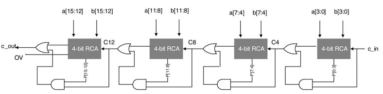
Figure 5.16 Conditional cell (CC)
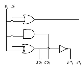
Here, ai and bi are the ith bits of operands a and b, s0i and c0i are the sum and carry-out bits at location i calculated by assuming 0 as carry-in, and similarly s1i and c1i are the sum and carry-out bits at location i that are computed by taking carry-in as 1. These equations are implemented by a logic cell called a condition cell (CC). A representative implementation of a CC is shown in Figure 5.16.
At level 2, the results from level 1 are merged together. This merging is done by pairing up consecutive columns at level 1. For an N -bit adder, the columns are paired as (i, i + 1) for i = 0, 1,...,N– 2. The least significant carry (LSC) bits at bit location i(i.e c0i and c1i ) in each pair selects the sum and carry bits at bit location i + 1 for the next level of processing. If the LSC bit is 0, then the bits computed for carry 0 are selected, otherwise the bits computed for carry 1 are selected for the next level. This level generates results as if a group of two bits are added assuming carry-in 0 and 1, as done in a carry select adder.
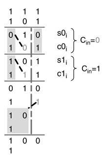
The example of Figure 5.17 illustrates the CSA by adding 3-bit numbers. In the first level each group consists of one bit each. The level adds bits at location i assuming carry-in of 0 and 1. In the next level, the three columns are divided into two groups. The column at bit location 0 forms the first group with the carry-in to the adder, and the rest of the two columns at bit location 1 and 2 form the second group. These two groups are separated with a dotted line in the figure. The selection of the appropriate bits in each group by the LSC is shown with a diagonal line. The LSC from each group determines which one of the two bits in the next column will be brought down to the next level of processing. If the LSC is 0, the upper two bits of the next column are selected, otherwise the lower two bits are selected for the next level. For the second group, the sum bit of the first column is also dropped down to the next level. The LSCs in the first level are shown with bold fonts. Finally in the next level the two groups formed in the previous level are merged and the LSC selects one of the two 3-bit group to the next level. In this example, as the LSC is one, it selects the lower group.
Figure 5.17 Addition of three bit numbers using a conditional sum adder
Example: The conditional sum adder technique will be further illustrated using a 16-bit addition. Figure 5.18 shows all the steps in computing the sum of two 16-bit numbers. Figure 5.19 lays out the architecture of the adder. At level 0, 16 CCs compute sum and carry bits assuming carry-in 0 and 1.
Figure 5.18 Example of a 16-bit conditional sum adder
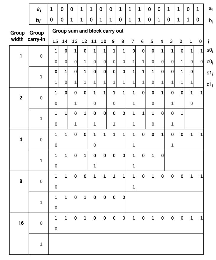
Figure 5.19 A 16-bit conditional sum adder
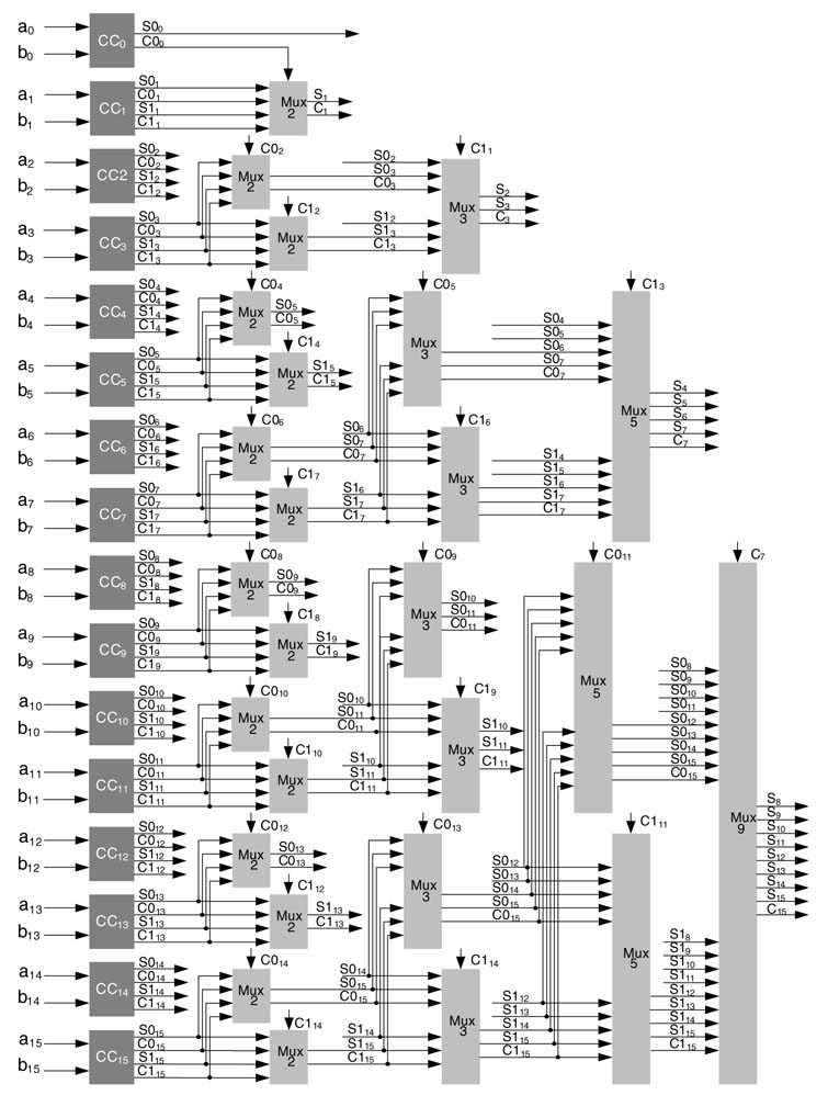
For this example the design assumes carry-in to the adder is 0, so CC0 is just a half adder that takes LSBs of the inputs, a0 and b0 and only computes sum and carry bits s00 and c00 for carry-in 0.The rest of the bits require addition for both carry-in 0and 1. CC1 takes a1 and b1 as inputs and computes sum and carry bits for both carry-in 0 (s01, c01) and 1 (s11, c11). Similarly, for each bit location i (= 1,..., 15), CCi computes sum and carry for both carry-in 0 (s0i, c0i) and 1 (s1i, c1i). For the next level, two adjacent groups of bit locations i and i + 1 are merged to form a new group. The LSC in each group is used to select one of the pairs of its significant bits for the next level. The process of merging the groups and selecting bits in each group based on LSC is repeated log2(16) = 4 times to get the final answer.
Verilog code for an 8-bit conditional sum adder is given here:
// Module for 8-bit conditional sum adder
module conditional_sum_adder
#(parameter W = 8)
// Inputs declarations
(input [W-1:0] a, b, // Two inputs a and b with a carry in cin
 input cin,
// Outputs declarations
output reg [W-1:0] sum, // Sum and carry cout output reg cout);
// Intermediate wires
wire s1_0, c2_0, s2_0, c3_0, s3_0, c4_0, s4_0, c5_0, s5_0, c6_0, s6_0,
 c7_0, s7_0, c8_0;
wire s1_1, c2_1, s2_1, c3_1, s3_1, c4_1, s4_1, c5_1, s5_1, c6_1, s6_1, c7_1,
 s7_1, c8_1;
// Intermediate registers
reg fcout;
reg s3_level_1_0, s3_level_1_1, s5_level_1_0, s5_level_1_1, s7_level_1_0,
 s7_level_1_1;
reg c4_level_1_0, c4_level_1_1, c6_level_1_0, c6_level_1_1, c8_level_1_0,
 c8_level_1_1;
reg c2_level_1;
reg c4_level_2;
reg s6_level_2_0, s6_level_2_1, s7_level_2_0, s7_level_2_1, c8_level_2_0,
 c8_level_2_1;
// Level 0
always @*
{fcout,sum[0]} = a[0] + b[0] + cin;
// Conditional cells instantiation
conditional_cell c1(a[1], b[1], s1_0, s1_1, c2_0, c2_1);
conditional_cell c2(a[2], b[2], s2_0, s2_1, c3_0, c3_1);
conditional_cell c3(a[3], b[3], s3_0, s3_1, c4_0, c4_1);
conditional_cell c4(a[4], b[4], s4_0, s4_1, c5_0, c5_1);
conditional_cell c5(a[5], b[5], s5_0, s5_1, c6_0, c6_1);
conditional_cell c6(a[6], b[6], s6_0, s6_1, c7_0, c7_1);
conditional_cell c7(a[7], b[7], s7_0, s7_1, c8_0, c8_1);

// Level 1 muxes
always @*
 case(fcout) // For first mux
 1’b0: {c2_level_1, sum[1]} = {c2_0, s1_0};
 1’b1: {c2_level_1, sum[1]} = {c2_1, s1_1};
 end case
always @* // For 2nd mux
case(c3_0)
 1’b0: {c4_level_1_0, s3_level_1_0} = {c4_0, s3_0};
 1’b1: {c4_level_1_0, s3_level_1_0} = {c4_1, s3_1};
 end case
always @* // For 3rd mux
case(c3_1)
 1’b0: {c4_level_1_1, s3_level_1_1} = {c4_0, s3_0};
 1’b1: {c4_level_1_1, s3_level_1_1} = {c4_1, s3_1};
 end case
always @* // For 4th mux
case(c5_0)
 1’b0: {c6_level_1_0, s5_level_1_0} = {c6_0, s5_0};
 1’b1: {c6_level_1_0, s5_level_1_0} = {c6_1, s5_1};
 end case
always @* // For 5th mux case(c5_1)
 1’b0: {c6_level_1_1, s5_level_1_1} = {c6_0, s5_0};
 1’b1: {c6_level_1_1, s5_level_1_1} = {c6_1, s5_1};
 end case
always @* // For 6th mux case(c7_0)
 1’b0: {c8_level_1_0, s7_level_1_0} = {c8_0, s7_0};
 1’b1: {c8_level_1_0, s7_level_1_0} = {c8_1, s7_1};
 end case
always @* // For 7th mux
case(c7_1)
 1’b0: {c8_level_1_1, s7_level_1_1} = {c8_0, s7_0};
 1’b1: {c8_level_1_1, s7_level_1_1} = {c8_1, s7_1};
 end case
// Level 2 muxes
always @* // First mux of level2
 case(c2_level_1)
 1’b0: {c4_level_2, sum[3], sum[2]} = {c4_level_1_0,
 s3_level_1_0, s2_0};
 1’b1: {c4_level_2, sum[3], sum[2]} = {c4_level_1_1,
 s3_level_1_1, s2_1};
 end case
 always @* // 2nd mux of level2
 case(c6_level_1_0)
 1’b0: {c8_level_2_0, s7_level_2_0, s6_level_2_0}
 = {c8_level_1_0, s7_level_1_0, s6_0};
 1’b1: {c8_level_2_0, s7_level_2_0, s6_level_2_0}
 ={c8_level_1_1, s7_level_1_1, s6_1};
 end case
always @*// 3rd mux of level2
 case(c6_level_1_1)
 1’b0: {c8_level_2_1, s7_level_2_1, s6_level_2_1}
 ={c8_level_1_0, s7_level_1_0, s6_0};
 1’b1: {c8_level_2_1, s7_level_2_1, s6_level_2_1}
 ={c8_level_1_1, s7_level_1_1, s6_1};
 end case
// Level 3 mux
always @*
 case(c4_level_2)
 1’b0: {cout,sum[7:4]} = {c8_level_2_0, s7_level_2_0,
 s6_level_2_0, s5_level_1_0, s4_0};
 1’b1: {cout,sum[7:4]} = {c8_level_2_1, s7_level_2_1,
 s6_level_2_1, s5_level_1_1, s4_1};
 end case
end module

// Module for conditional cell
module conditional_cell (a, b, s_0, s_1, c_0, c_1);
input a,b;
output s_0, c_0, s_1, c_1;
assign s_0 = a^b; // sum with carry in 0
assign c_0 = a&b; // carry with carry in 0
assign s_1 = ~s_0; // sum with carry in 1
assign c_1 =a|b; // carry with carry in 1
end module
5.5.10 Carry Select Adder
The carry select adder (CSA) is not as fast as the carry look-ahead adder and requires considerably more hardware if mapped on custom ASICs, but it has a favorable design for mapping on an FPGA with fast carry chain logic. Te CSA partitions an N -bit adder into K groups, where:
where N k represents the number of bits in group k. The basic idea is to place two N k-bit adders at each stage k. One set of adders computes the sum by assuming a carry-in 1, and the other a carry-in 0. The actual sum and carry are selected using a 2-to-1 MUX (multiplexer) based on the carry from the previous group.
Figure 5.20 shows a 16-bit carry select adder. The adder is divided into four groups of 4-bits each. As each block is of equal width, their outputs will be ready simultaneously. In an unequal-width CSA the block size at any stage in the adder is set larger than the block size at its less significant stage. This helps in reducing delay further as the carry-outs in less significant stages are ready to select the sum and carry of their respective next stages.
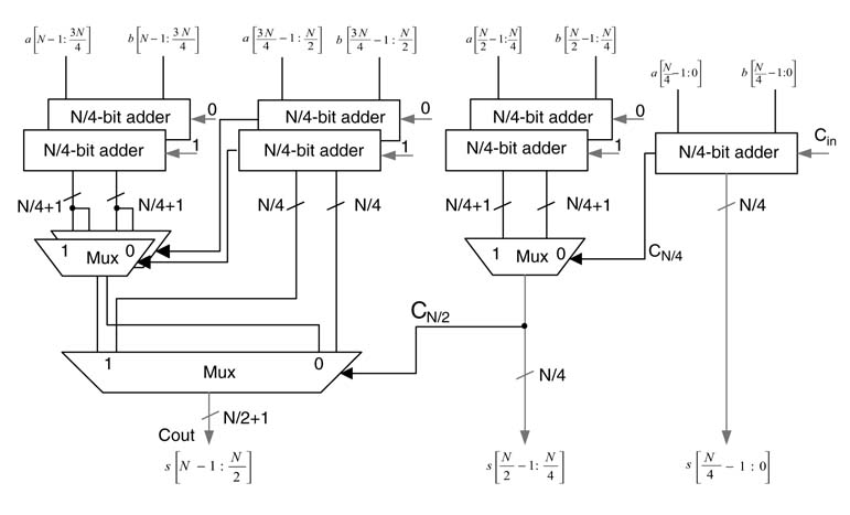
The CSA can be broken down into more than one stage. Figure 5.21 shows a two-stage CSA. The N -bit adder is divided into two groups of size N/2 bits. Each stage is further divided into two subgroups of N/4 bits. In the first stage each subgroup computes sums and carries for carry-in 0 and 1 and two subgroups are merged inside a group. Then, in the second stage, two groups are merged and final sums and carry-out are generated. Interestingly if we keep breaking the groups into more levels until each group contains one bit each, the adder architecture will be the same as for a conditional sum adder. This reveals that a conditional sum adder is a special case of a hierarchical CSA. The RTL Verilog code for a 16-bit hierarchical CSA is given here:
module HierarchicalCSA(a, b, cin, sum, c_out);
input [15:0] a,b;
input cin;
output c_out;
output [15:0] sum;
wire c4, c8, c8_0, c8_1, c12_0, c12_1, c16_0, c16_1, c16L2_0, c16L2_1;
wire [15:4] sumL1_0, sumL1_1;
wire [15:12] sumL2_0, sumL2_1;

// Level one of hierarchical CSA assign {c4,sum[3:0]} = a[3:0] + b[3:0] + cin;
assign {c8_0, sumL1_0[7:4]}= a[7:4] + b[7:4] + 1’b0;
assign {c8_1, sumL1_1[7:4]}= a[7:4] + b[7:4] + 1’b1;
assign {c12_0,sumL1_0[11:8]}= a[11:8] + b[11:8] + 1’b0;
assign {c12_1,sumL1_1[11:8]}= a[11:8] + b[11:8] + 1’b1;
assign {c16_0, sumL1_0[15:12]}= a[15:12] + b[15:12] + 1’b0;
assign {c16_1, sumL1_1[15:12]}= a[15:12] + b[15:12] + 1’b1;

// Level two of hierarchical CSA
assign c8 = c4 ? c8_1: c8_0;
assign sum[7:4] = c4 ? sumL1_1[7:4]: sumL1_0[7:4];

// Selecting sum and carry within a group
assign c16L2_0 = c12_0 ? c16_1: c16_0;
assign sumL2_0 [15:12] = c12_0? sumL1_1[15:12]: sumL1_0[15:12];
assign c16L2_1 = c12_1 ? c16_1: c16_0;
assign sumL2_1 [15:12] = c12_1? sumL1_1[15:12]: sumL1_0[15:12];

// Level three selecting the final outputs
assign c_out = c8 ? c16L2_1: c16L2_0;
assign sum[15:8] = c8 ? {sumL2_1[15:12], sumL1_1[11:8]}:
 {sumL2_0[15:12], sumL1_0[11:8]};
end module
Figure 5.20 A 16-bit uniform-groups carry select adder
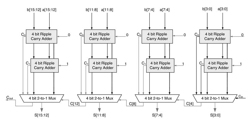
Figure 5.21 Hierarchical CSA
5.5.11 Using Hybrid Adders
A digital designer is always confronted with finding the best design option in area-power-time tradeoffs. A good account of these tradeoffs is given in [10]. The designer may find it appropriate to divide the adder into multiple groups and use different adder architecture for each group. This may help the designer to devise an optimal adder architecture for the design. This design methodology is discussed in [10] and [11].
5.6 Barrel Shifter
A single-cycle N -bit logic shifter implementing x≫s , where s is a signed integer number, can be implemented by hardwiring all the possible shift results as input to a multiplexer and then using s to select the appropriate option at the output. The shifter performs a shift left operation for negative values of s. For example, x ≫–2 implies a shift left by 2.
The design of the shifter is shown in Figure 5.22(a), where x is the input operand and all possible shifts are pre-performed as input to the MUX and s is used as a select line to the MUX. The figure clearly shows that, for negative values of s, its equivalent positive number will be used by the MUX for selecting appropriate output to perform a shift left operation.
The design can be trivially extended to take care of arithmetic along with the logic shifts. This requires first selecting either the sign bit or 0 for appropriately appending to the left of the operand for shift right operation. For shift left operation, the design for both arithmetic and logic shift is same. When there are not enough redundant sign bits, the shift left operation results in overflow. The design of an arithmetic and logic shifter is given in Figure 5.22(b).
Instead of using one MUX with multiple inputs, a barrel shifter can also be hierarchically constructed. This design can also be easily pipelined. The technique can work for right as well as for left shift operations. For x ≫s , the technique works by considering s as a two’s complement signed number where the sign bit has negative weight and the rest of the bits carry positive weights. Moving from MSB to LSB, each stage of the barrel shifter only caters for one bit and performs the requisite shift equal to the weight of the bit.
Figure 5.22 Design of Barrel Shifters (a) An arithmetic shifter for an 8-bit signed operand. (b) A logic and arithmetic shifter for an 8-bit operand
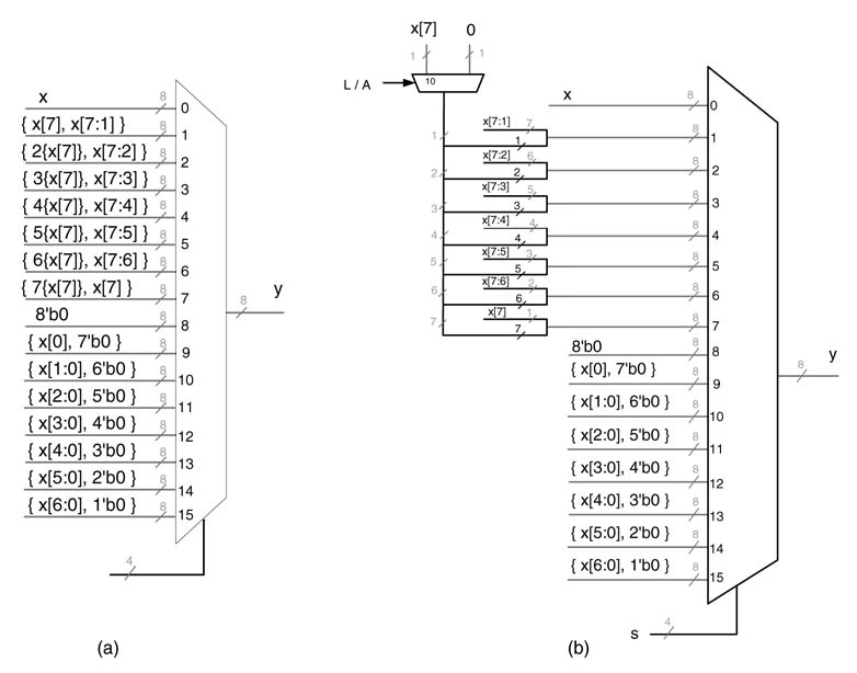
Figure 5.23 shows a barrel shifter for shifting a 16-bit number x by a 5-bit signed number s . Thus the barrel shifter can perform shifts from 0 to 15 to the right and 1 to 16 to the left in five stages or levels. First the shifter checks whether the logic or arithmetic shift is required and appropriately selects 0 or the sign bit of the operand for further appending for shift right operation. The barrel shifter then checks the MSB of s , as this bit has negative weight. Therefore, if s [4] = 1, the shifter performs a shift left by 16 and keeps the result as a 31-bit number; otherwise, for s [4]=0,the number is appropriately extended to a 31-bit number for the next levels to perform appropriate shifts. For the rest of thes the logic performs a shift right operation equal to the weight of the bit under consideration, and the design keeps reducing the number of bits to the width required at the output of each stage. The design of this hierarchical barrel shifter is shown in Figure 5.23(a) and its RTL Verilog code is given here:
module Barrel Shifter(
input [15:0] x,
input signed [4:0] s,
input A_L, output reg [15:0]y);
reg [30:0] y0;
reg [22:0] y1;
reg [18:0] y2;
reg [16:0] y3;
reg [14:0] sgn;
always @(*)
begin
// A_L =1 for Arithmetic and 0 for Logical shift
 sgn = (A_L) ? {15{x[15]}} : 15’b0;
 y0 = (s [4]) ? {x[14:0],16’b0} : {sgn[14:0], x[15:0]};
 y1 = (s[3]) ? y0[30:8] : y0[22:0];
 y2 = (s[2]) ? y1[22:4] : y1[18:0];
 y3 = (s[1]) ? y2[18:2] : y2[16:0];
 y = (s[0]) ? y3[16:1] : y3[15:0];
end
endmodule
This design can be easily pipelined by placing registers after any number of multiplexers and appropriately delaying the respective selection bit for coherent operation.Afully pipelined design of a barrel shifter is given in Figure 5.23(b), and the code for RTLVerilog implementation of the design is listed here:
Figure 5.23 Design of a barrel shifter performing shifts in multiple stages. (a) Single-cycle design. (b) Pipelined design
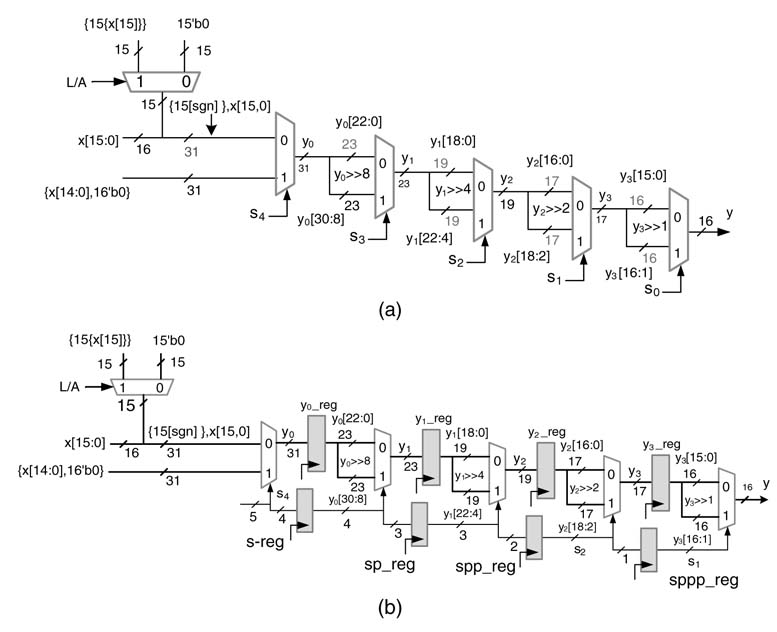
module BarrelShifterPipelined(
input clk,
input [15:0] x,
input signed [4:0] s,
input A_L,
outputreg [15:0]y);
reg [30:0] y0, y0_reg;
reg [22:0] y1, y1_reg;
reg [18:0] y2, y2_reg;
reg [16:0] y3, y3_reg;
reg [14:0] sgn;
reg [3:0] s_reg;
reg [2:0] sp_reg;
reg [1:0] spp_reg;
reg sppp_reg;

always @(*)
begin
// A_L =1 for arithmetic and 0 for logical shift
 sgn = (A_L) ? {15{x[15]}}: 15’b0;
 y0= (s [4]) ? {x[14:0],16’b0}: {sgn[14:0], x[15:0]};
 y1= (s_reg[3]) ? y0_reg[30:8]: y0_reg[22:0];
 y2 = (sp_reg[2]) ? y1_reg[22:4]: y1_reg[18:0];
 y3 = (spp_reg[1]) ? y2_reg[18:2]: y2_reg[16:0];
 y= (sppp_reg) ? y3_reg[16:1]: y3_reg[15:0];
end
always @ (posedge clk)
begin
 y0_reg <= y0;
 y1_reg <= y1;
 y2_reg <= y2;
 y3_reg <= y3;
 s_reg <= s[3:0];
 sp_reg <= s_reg [2:0];
 spp_reg <= sp_reg [1:0];
 sppp_reg <= spp_reg [0];
end
end module
A barrel shifter can also be implemented using a dedicated multiplier in FPGAs. A shift by s to the left is multiplication by 2s, and similarly a shift to the right by s is multiplication by 2-s. To accomplish the shift operation, the number can be multiplied by an appropriate power of 2 to get the desired shift.
Example: Assume x is a signed operand in Q1.7 format. Let:
x ≫3 can be performed by multiplying x by y = 2-3, which in Q1.7 format is equivalent to y = 8’b0001_0000. The fractional multiplication of x by y results in a Q2.14 format number:
14’b1111_1001_0101_0000. On dropping the redundant sign bit and 7 LSBs, as is done in fractional signed multiplication, the shift results in an 8-bit number:
Following the same rationale, both arithmetic and logic shifts can be performed by appropriately assigning the operands to a dedicated multiplier embedded in FPGAs.
5.7 Carry Save Adders and Compressors
5.7.1 Carry Save Adders
This chapter has discussed various architectures for adding numbers. These adders, while adding two operands, propagate carries from one bit position to the next in computing the final sum and are collectively known as carry propagate adders (CPAs). Although three numbers can be added in a single cycle by using two CPAs, a better option is to use a carry save adder (CSA) that first reduces the three numbers to two and then any CPA adds the two numbers to compute the final sum. From the timing and area perspective, the CSA is one of the most efficiently and widely used techniques for speeding up digital designs of signal processing systems dealing with multiple operands for addition and multiplication. Several dataflow transformations are reported that extract and transform algorithms to use CSAs in their architectures for optimal performance [13].
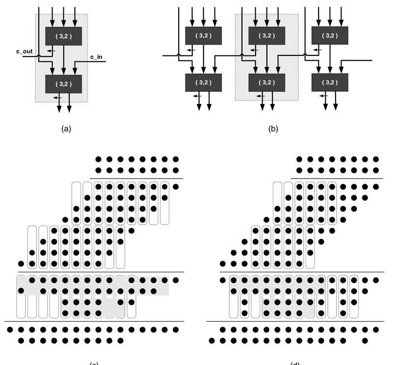
A CSA, while reducing three operands to two, does not propagate carries; rather, a carry is saved to the next significant bit position. Thus this addition reduces three operands to two without carry propagation delay. Figure 5.24 illustrates addition of three numbers. As this addition reduces three numbers to two numbers, the CSA is also called a 3:2 compressor.
5.7.2 Compression Trees
There are a host of techniques that effectively use CSAs to add more than three operands. These techniques are especially attractive for reducing the partial products in multiplier design. Section 5.8 covers the use of these techniques in multiplier architectures, and then mentions their use in optimizing many signal processing architectures and applications.
5.7.3 Dot Notation
Dot notation is used to explain different reduction techniques. In this notation each bit in a multi-bit operands addition is represented by a dot. Figure 5.25 shows four dots to represent four bits of PP[0] in a 4 x 4-bit multiplier. The dots appearing in a column are to be added for computing the final product. A reduction technique based on a 3:2 compressor reduces three layers of PPs to two. The technique considers the number of dots in each column. If an isolated dot appears in a column, it is simply dropped down to the next level of logic. When there are two dots in a column, then they are added using a half adder, where the dot for the sum is simply dropped down in the same column and the dot for the carry is placed in the next significant column. Use of a half adder in this reduction is also known as a 2:2 compressor. The three dots in a column are reduced to two using a full adder. The dot for the sum is placed at the same bit location and the dot for the carry is moved to the next significant bit location. Figure 5.26 shows these three cases of dot processing.
Figure 5.24 Carry save addition saves the carry at the next bit location
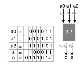
Figure 5.25 Dots are used to represent each bit of the partial product
5.8 Parallel Multipliers
5.8.1 Introduction
Most of the fundamental signal processing algorithms use multipliers extensively. Keeping in perspective their importance, the FPGAvendors are embedding many dedicated multipliers. It is still very important to understand the techniques that are practised for optimizing the implementation of these multipliers. Although a sequential multiplier can be designed that takes multiple cycles to compute its product, multiplier architectures that compute the product in one clock cycle are of interest to designers for high-throughput systems. This section discusses parallel multipliers.
A CSA is one of the fundamental building blocks of most parallel multiplier architectures. The partial products are first reduced to two numbers using a CSA tree. These two numbers are then added to get the final product. Many FPGAs have many dedicated summers. The summer can add three operands. The reduction trees can reduce the number of partial products to three instead of two to make full use of this block.
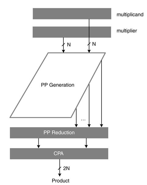
Any parallel multiplier architecture consists of three basic operations: partial product generation, partial product reduction, and computation of the final sum using a CPA, as depicted in Figure 5.27. For each of these operations, several techniques are used to optimize the HW of a multiplier.
Figure 5.26 Reducing the number of dots in a column
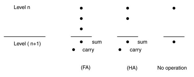
Figure 5.27 Three components of a multiplier
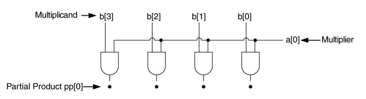
5.8.2 Partial Product Generation
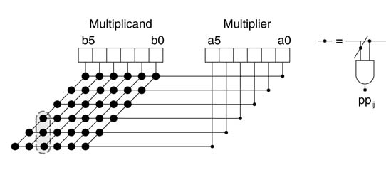
While multiplying two N -bit unsigned numbers a and b, the partial products (PPs) are generated either by using an ANDing method or by implementing a modified Booth recoding algorithm. The first method generates partial product PP[i] by ANDing each bit ai of the multiplier with all the bits of the multiplicand b. Figure 5.28 shows the generation of partial products for a 6 x 6 multiplier. Each PP[i] is shifted to the left by i bit positions before the partial products are added columN -wise to produce the final product.
Figure 5.28 Partial-product generation for a 6 x 6 multiplier
Verilog code for a 6 x 6 unsigned multiplier is given below. The implementation only highlights the partial product generation and does not use any PP reduction techniques. These PPs are appropriately shifted by using a concatenation operator in Verilog and then added to complete the functionality of the multiplier module. The second technique of partial product generation, called modified Booth recoding, is discussed in Section 5.9.4.
module multiplier
(
input [5:0] a,b,
output [11:0] prod);
integer i;
reg [5:0] pp [0:5];//6 partial products
always@*
begin
 for(i=0; i<6; i=i+1)
 begin
 pp[i] = b & {6{a[i]}};
 end
end
 assign prod = pp[0]+{pp[1],1’b0}+{pp[2],2’b0} +
 {pp[3],3’b0}+{pp[4],4’b0}+{pp[5],5’b0};
endmodule
5.8.3 Partial Product Reduction
While multiplying an N 1 -bit multiplier a with an N 2-bit multiplicand b, N1 PPs are produced by ANDing each bit a[i] of the multiplier with all the bits of the multiplicand and shifting the partial product PP[i] to the left by i bit positions. Using dot notations to represent bits, all the partial products form a parallelogram array of dots. These dots in each column are to be added to compute the final product. For a general N 1 x N 2 multiplier, the following four techniques are generally used to reduce N 1 layers of the partial products to two layers for their final addition using any CPA:
- carry save reduction
- dual carry save reduction
- Wallace tree reduction
- Dadda tree reduction.
Although the techniques are described here for 3:2 compressors, the same can be easily extended for other compressors and counters.
5.8.3.1 Carry Save Reduction
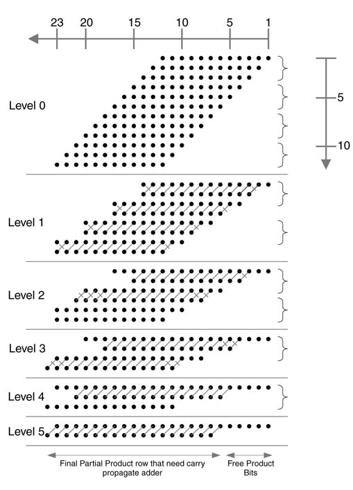
The first three layers of the PPs are reduced to two layers using carry save addition (CSA). In this reduction process, while generating the next level of logic, isolated bits in a column, in the selected three layers, are simply dropped down to the same column, columns with two bits are reduced to two bits using half adders and the columns with three bits are reduced to two bits using full adders. While adding bits using HAs or FAs, the dot representing the sum bit is dropped down in the same column whereas the dot representing the carry bit is placed in the next significant bit column. Once the first three partial products are reduced to two layers, the fourth partial product in the original composition is grouped with them to make a new group of three layers. These three layers are again reduced to two layers using the CSA technique. The process is repeated until the entire array is reduced to two layers of numbers. This scheme results in a few least significant product bits (called free product bits), and the rest of the bits appear in two layers, which are then added using any CPA to get the rest of the product bits.
Figure 5.29 shows carry save reduction scheme for reducing twelve PPs resulting from multiplication of two 12-bit numbers to two layers. At level 0, the first three PPs are selected. The first and the last columns in this group contain only 1 bit each. These bits are simply dropped down to level 1 without performing any operation. The two bits of the second and the second last columns are reduced using HAs. As the rest of the columns contain three bits each, FAs are used to reduce these bits to 2 bits each, where sum bits are placed in the same columns and carry bits are placed in the next columns of level 1. This placement of carries in the next columns is shown by diagonal lines. The use of an HA is shown by across line. In level1,two least significant final product bits are produced (free product bits). In level 1 the two layers produced by reduction of level 0 are further grouped with the fourth PP and the process of reduction is repeated. For 12 layers of PPs, it requires 10 levels to reduce the PPs to two layers.
Figure 5.29 PP reduction for a 12 x 12 multiplier using a carry save reduction scheme
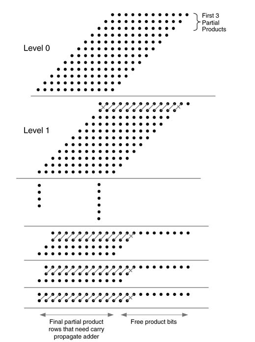
Figure 5.30 Carry save reduction scheme layout for a 6 x 6 multiplier
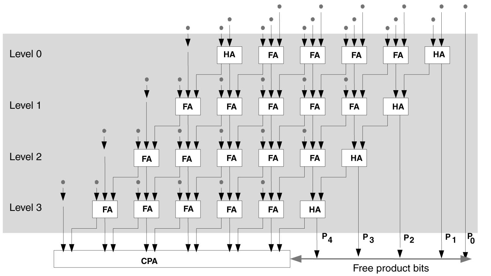
Figure 5.30 shows a layout of carry save reduction for reducing PPs of a 6 x 6 multiplier. The layout clearly shows use of HAs and FAs and production of free bits. There are four levels of logic and each level reduces three layers to two.
5.8.3.2 Dual Carry Save Reduction
The partial products are divided into two equal-size sub-groups. The carry save reduction scheme is applied on both the sub-groups simultaneously. This results in two sets of partial product layers in each sub-group. The technique finally results in four layers of PPs. These layers are then reduced as one group into three, and then into two layers.
5.8.3.3 Wallace Tree Reduction
Partial products are divided into groups of three PPs each. Unlike the linear time array reduction of the carry save and dual carry save schemes, these groups of partial products are reduced simultaneously using CSAs. Each layer of CSAs compresses three layers to two layers. These two layers from each group are re-grouped into a set of three layers. The next level of logic again reduces three-layer groups into two layers. This process continues until only two rows are left. At this stage any CPA can be used to compute the final product.
Figure 5.31 shows the implementation of Wallace tree reduction of 12 partial products. The PPs are divided into four groups of three PPs each. In level 0, carry save reduction is applied on each group simultaneously. Each group reduces its three layers to two layers, and as a result eight layers are produced. These eight layers are further grouped into three PPs each; this forms two groups of three layers each, and two layers are left as they are. In level 1, these two groups of three layers are further reduced using carry save addition, and this produces four layers. These four layers are combined with the two layers that are not processed in the previous level. Now in level 2 there are six layers; they form two groups of three layers and are reduced to four layers. Only one group is formed at this stage. Repeating the reduction process twice will reduce the number of layers to three and then two. The final two layers can then be added using any CPA to produce the final product.
Figure 5.31 Wallace reduction tree applied on 12 PPs
Wallace reduction is one of the most commonly used schemes in multiplier architecture. It falls into the category of log time array multiplier as the reduction is performed in parallel in groups of threes and this results only in a logarithmic increase in the number of adder levels as the number of PPs increases (i.e. the size of the multiplier increases). The number of adder levels accounts for the critical path delay of the combinational cloud. Each adder level incurs one FA delay in the path. Table 5.3 shows the logarithmic increase in the adder levels as the number of partial products increases. As the Wallace reduction works on groups of three PPs, the adder levels are the same for a range of number of PPs. For example, if the number of PPs is five or six, it will require three adder levels to reduce the PPs to two layers for final addition.
Example: Figure 5.32 shows the layout of the Wallace reduction scheme on PP layers for a 6 x 6 multiplier of the reduction logic. In level 0, the six PPs are divided into two groups of three PPs each.
Table 5.3 Logarithmic increase in adder levels with increasing number of partial products
| Number of PPs | Number of full-adder delays |
| 3 | 1 |
| 4 | 2 |
| 5 ≤ n ≤ 6 | 3 |
| 7 ≤ n ≤ 9 | 4 |
| 10 ≤ n ≤ 13 | 5 |
| 14 ≤ n ≤ 19 | 6 |
| 20 ≤ n ≤ 28 | 7 |
| 29 ≤ n ≤ 42 | 8 |
| 43 ≤ n ≤ 63 | 9 |
The Wallace reduction reduces these two groups into two layers of PPs each. These four layers are reduced to two layers in two levels of CSA by further grouping and processing them through carry save addition twice.
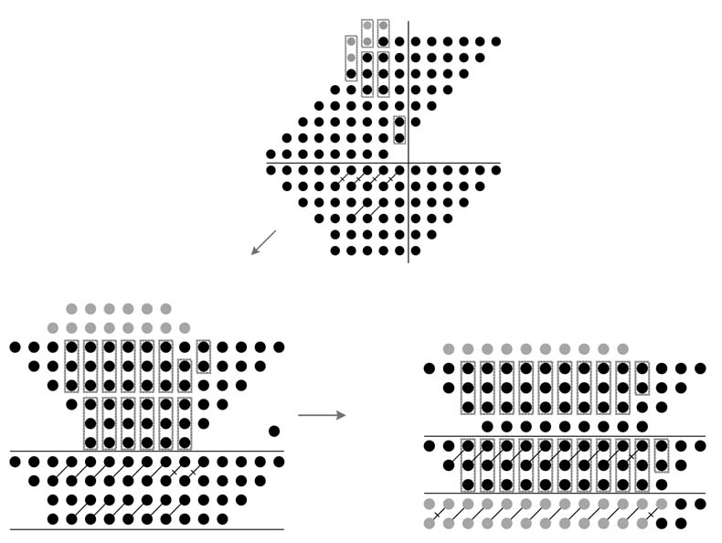
5.8.3.4 Dadda Tree Reduction
The Dadda tree requires the same number of adder levels as the Wallace tree, so the critical path delay of the logic is the same. The technique is useful as it minimizes the number of HAs and FAs at each level of the logic.
Figure 5.32 Wallace reduction tree layout for a 6 x 6 array of PPs
Consider the following sequence from a Wallace tree reduction scheme given as the upper limit of column 1 in Table 5.3:
Each number represents the maximum number of partial products at each level that requires a fixed number of adder levels. The sequence also depicts that two partial products can be obtained from at most three partial products, three can be obtained from four, four from six, and so on.
The Dadda tree reduction considers each column separately and reduces the number of logic levels in a column to the maximum number of layers in the next level. For example, reducing PPs in a 12 x 12-bit multiplier, Wallace reduction reduces 12 partial products to eight whereas the Dadda scheme first reduces them to the maximum range in next the group, and this is nine as reducing twelve layers to eight will require the same number of logic levels as eight but results in less hardware.
In the Dadda tree each column is observed for the number of dots. If the number of dots in a column is less than the maximum number of PPs required to be reduced in the current level, they are simply dropped down to the next level of logic without any processing. Those columns that have more dots than the required dots for the next level are reduced to take the maximum layers in the next level.
Example: Figure 5.33 shows Dadda reduction on an 8 x 8 partial-product array. From Table 5.3 it is evident that eight PPs should be reduced to six PPs. In level 0, this reduction scheme leaves the columns that have less than or equal to six dots and only apply reduction on columns with more than six dots. The columns having more than six dots are reduced to six. Thus the first six columns are dropped down to the next level without any reduction. Column 7 has seven dots; they are reduced to six by placing a HA. This operation generates a carry in column 8, which is shown in gray in the figure. Column 8 will then have nine dots. An HA and an FA reduce these nine dots to six and generate two carries in column 9. Column 9 will have nine dots, which are again reduced to six using an HA and an FA. (HAs and FAs are shown in the figure with diagonal crossed and uncrossed lines, respectively.) Finally, column 10 will reduce eight dots to six using an FA. The maximum number of dots in any column in the next level is six. For the next level, Table 5.3 shows that six PPs should be reduced to four. Each column is again observed for potential reduction. The reduction is only applied if the total number of dots, including dots coming from the previous column, is four or more, and these dots are reduced to three. The process is repeated to reduce three dots to two. This process is shown in Figure 5.33.
Figure 5.33 Dadda reduction levels for reducing eight PPs to two
5.8.4 A Decomposed Multiplier
A multiplication can be decomposed into a number of smaller multiplication operations. For example, 16 x 16-bit multiplication can be performed by considering the two 16-bit operands a and b as four 8-bit operands, where aH and aL are eight MSBs and LSBs of a, and bH and bL are eight MSBs and LSBs of b. Mathematical decomposition of the operation is given here:
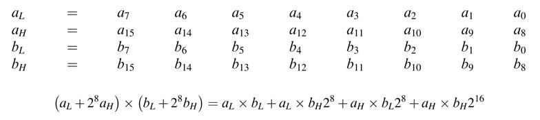
A 16 x 16-bit multiplier can be constructed to perform these four 8 x 8-bit multiplications in parallel. The results of these are then combined to compute the product of the multiplier.
Figure 5.34(a) shows the decomposition of a 16 x 16-bit multiplier into four 8 x 8-bit multipliers. The results of these four multipliers are appropriately added. Figure 5.34(b) shows the reduction of the four products using a reduction technique for final addition. This decomposition technique is very useful in designs where either four 8 x 8 or one 16 x 16 multiplication is performed.
Figure 5.34 (a) A 16 x 16-bit multiplier decomposed into four 8 x 8 multipliers. (b) The results of these multipliers are appropriately added to get the final product
5.8.5 Optimized Compressors
Based on the concept of CSA, several other compressor blocks can be developed. For example a 4:2 compressor takes four operands and 1 bit for the carry-in and reduces them to 2 bits in addition to a carry-out bit. A candidate implementation of the compressor is shown in Figure 5.35(a). While compressing multiple operands the compressor works in cascade and creates an extended tile, as shown in Figure 5.35(b).
The use of this compressor in Wallace and Dadda reduction trees for an 8 x 8-bit multiplier is shown in Figure 5.35(c) and Figure 5.35(d). This compressor, by using carry-chain logic, is reported to exhibit better timing and area performance compared with a CSA-based compression on a Virtex FGPA [14]. Similarly, a 5:3 bit counter reduces 5 bits to 3 bits with a carry-in and carry-out bit and is used in designing multiplier architectures in [15].
Figure 5.35 (a) Candidate implementation of a 4:2 compressor. (b) Concatenation of 4:2 compression to create wider tiles. (c) Use of a 4:2 compressor in Wallace tree reduction of an 8 x 8 multiplier. (d) Use of a 4:2 compressor in an 8 x 8 multiplier in Dadda reduction
5.8.6 Single- and Multiple-column Counters
Multi-operand additions on ASIC are traditionally implemented using CSA-based Wallace and Dadda reduction trees. With LUTs and carry chaiN -based FPGA architecture in mind, the counter-based implementation offers a better alternative to CSA-based multi-operand addition on FPGAs [16]. These counters add all bits in single or multiple columns to best utilize FGPA resources.
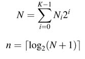
A single-column N:n counter adds all N bits in a column and returns an N -bit number, where n = log2(N + 1). Early FPGA architectures were 4-input LUT-based designs. Recently, 6-input LUTs with fast carry-chain logic have appeared in the Vertix™-4 and Virtex™-5 families. A design that effectively uses these features is more efficient than the others. A 6:3 counter fully utilizing three 6-input LUTs and carry-chain logic has been shown to outperform other types of compressors for the Virtex™-5 family of FPGAs [17]. A 6:3 counter compressing six layers of multi operands to three layers is shown in Figure 5.36(a). The design uses three 6-input LUTs while compressing six layers to three, as shown in Figure 5.36(b). Each LUT computes respective sum, carry0 and carry1 bits of the compressor.
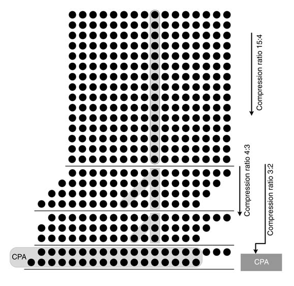
Counters of different dimensions can also be built, and a mixture of these can be used to reduce multiple operands to two. Figure 5.37 shows 15:4, 4:3 and 3:2 counters working in cascade to compress a 15 x 15 matrix.
In a multi-operand addition operation, a generalized parallel counter (GPC) adds number of bits in multiple adjacent columns. A K -column GPC adds N 0, N1,… , N K-1 bits in least significant 0 to most significant column K–1, respectively, and produces an n -bit number, where:
The example of Figure 5.38 shows a (3,4,5:5) counter. The counter compresses 3,4 and 5 bits in columns 0, 1and 2, respectively, and produces one bit each in bit locations 0, 1, 2, 3 and 4. Similarly, Figure 5.39 shows a compression of two columns of 5 bits each into a 4-bits (5,5:4) counter.
Figure 5.36 Single column counter (a) A 6:3 counter reducing six layers of multiple operands to three. (b) A 6:3 counter is mapped on three 6-input LUTs for generating sum, carry 0 and carry 1 output
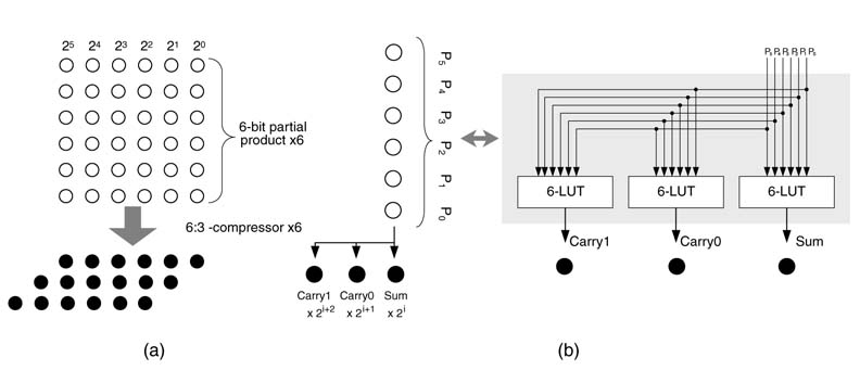
Figure 5.37 Counters compressing a 15 x 15 matrix
GPC offers flexibility once mapped onto a FPGA. The problem of configuring dimensions of GPC for mapping on FPGA for multi-operand addition is an NP-complete problem. The problem is solved using ‘integer programming’, and the method is reported to outperform adder tree-based implementation from the area and timing perspectives [18].
As stated earlier, FGPAs are best suited for counters and GPC-based compression trees. To fully utilize 6-LUT-based FPGAs, it is better that each counter or GPC should have six input bits and three (or preferably four) output bits, as shown in Figure 5.40 and Figure 5.41. The four output bits are favored as the LUTs in many FPGAs come in groups of two with shared 6-bit input, and a 6:3 GPC would waste one LUT in every compressor, as shown in Figure 5.41(a).
Figure 5.38 A (3,4,5:5) GPC compressing three columns with 3, 4 and 5 bits to 5 bits in different columns
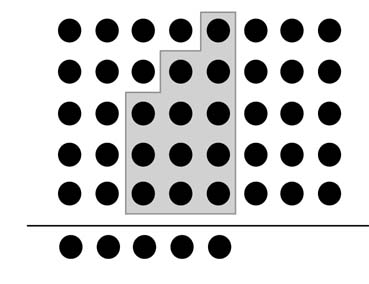
Figure 5.39 Compressor tree synthesis using compression of two columns of 5 bits each into 4-bit (5,5;4) GPCs
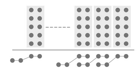
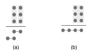
Figure 5.40 Compressor tree mapping by (a) 3:2 counters, and (b) a (3,3;4) GPC
5.9 Two’s Complement Signed Multiplier
5.9.1 Basics
This section covers architectures that implement signed number multiplications. Recollecting the discussion in Chapter 3 on two’s complement numbers, an N -bit signed number x is expressed as:
Figure 5.41 (a) The Altera FPGA adaptive logic module (ALM) contains two 6-LUTs with shared inputs; 6-input 3-output GPC has 3/4 logic utilization (b) A 6-input 4-output GPC has full logic utilization
where xn -1 is the MSB that carries negative weight. When we multiply an N 1-bit signed multiplier a with an N 2-bit signed multiplicand b, we get N 1 partial products. For the first N 1-1 partial products, the PP[i] is obtained by ANDing bit ai of a with b and shifting the result by i positions to the left, This implements multiplication of b with ai2i:
The PP[i] in the above expression is just the signed multiplicand that is shifted by i to the left, so MSBs of all the partial products have negative weights. Furthermore, owing to the shift by i, all these PPs are unequal-width signed numbers. All these numbers are needed to be left-aligned by sign extension logic before they are added to compute the final product.
Now we need to deal with the last PP. As the MSB of a has negative weight, the multiplication of this bit results in a PP that is two’s complement of the multiplicand. PP[N 1- i] is computed as
All these N 1 partial products are appropriately sign extended and added to get the final product.
Example: Figure 5.42 shows 4 x 4-bit signed by signed multiplication. The sign bits of the first three PPs are extended and shown in bold. Also note that the two’s complement of the last PP is taken to cater for the negative weight of the MSB of the multiplier. As can be seen, if the signed by signed multiplier is implemented as in this example, the sign extension logic will take significant area of the compression tree. It is desired to somehow remove this logic from the multiplier.
5.9.2 Sign Extension Elimination
A simple observation in a sign extended number leads us to an effective technique for elimination of sign extension logic. An equivalent of the sign extended number is computed by flipping the sign bit and adding a 1 at the location of the sign bit and extending the number with all 1s. Figure 5.43(a) explains the computation on a positive number. The sig N -bit 0 is flipped to 1 and a 1 is added at the sig N -bit location and extended bits are replaced by all 1s. This technique equivalently working on negative numbers is shown in Figure 5.43(b). The sig N -bit 1 is flipped to 0 and a 1 is added to the sig N -bit location and the extended bits are all 1s. Thus, irrespective of the sign of the number, the technique makes all the extended bits into 1s. Now to eliminate the sign extension logic, all these 1s are added off-line to form a correction vector.
Figure 5.42 Showing 4 x 4-bit signed by signed multiplication
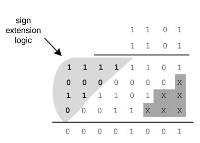
Figure 5.43 sig N -extension elimination
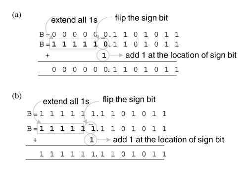
Figure 5.44 illustrates the steps involved in sig N -extension elimination logic on a 11 x 6-bit signed by signed multiplier. First the MSB of all the PPs except the last one are flipped and a 1 is added at the sig N -bit location, and the number is extended by all 1s. For the last PP, the two’s complement is computed by flipping all the bits and adding 1 to the LSB position. The MSB of the last PP is flipped again and 1 is added to this bit location for sign extension. All these 1s are added to find a correction vector (CV). Now all the 1s are removed and the CV is simply added and it takes care of the sign extension logic.
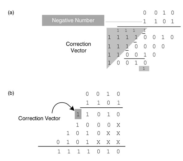
Example: Find the correction vector for a 4 x 4-bit signed multiplier and use the CV to multiply two numbers 0011 and 1101. In Figure 5.45(a), all the 1s for sign extension and two’s complement are added and CV= 0001_0000. Applying sig N -extension elimination logic and adding CV to the PPs, the multiplication is performed again and it gives the same result, as shown in Figure 5.45(b). As the correction vector has just one no N -zero bit, the bit is appended with the first PP (shown in gray).
Figure 5.44 sig N -extension elimination and CV formulation for signed by signed multiplication
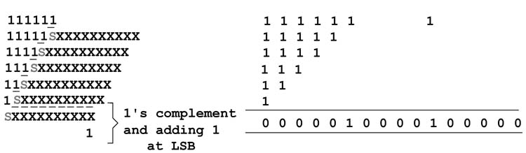
Figure 5.45 Multiplying two numbers, 0011 and 1101
Hardware implementation of a signed by signed multiplication using the sig N -extension elimination technique saves area and thus is very effective.
5.9.3 String Property
So far we have represented numbers in two’s complement form, where each bit is either a 0 or 1. There are, of course, other ways to represent numbers. A few of these are effective for hardware design for signal processing systems. Canonic signed digit (CSD) is one such format [19-21]. In CSD, a digit can be a 1, 0 or –1. The representation restricts the occurrence of two consecutive no N -zeros in the number, so it results in a unique representation with minimum number of nonzero digits.
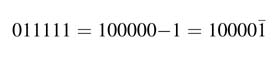
The CSD of a number can be computed using the string property of numbers. This property, while moving from LSB to MSB, successively observes strings of 1s and replaces each string with an equivalent value, using 1, 0 or –1. Consider the number 7. This can be written as 8 – 1, or in CSD representation:
The bit with a bar over has negative weight and the others have positive weights. Similarly, 31 can be written as 32 – 1, or in CSD representation:
Thus, equivalently, a string of 1s is replaced with 1 at the least significant ī of the string, and a 1 placed next to the most significant 1 of the string, while all other bits are filled with zeros.
We can trivially extend this transformation to any string of 1s in binary representation of a number. The string property can be recursively applied on binary representations of a number. The transformed number has minimum number of no N -zero bits. The representation and its use in digital design are further discussed in Chapter 6.
The example in Figure 5.46 shows how the string property can be recursively applied. The number of no N -zero digits in the example has reduced from 14 to 6.
5.9.4 Modified Booth Recoding Multiplier
The three basic building blocks of a multiplier are the generation of PPs, reduction of PPs to two layers, and addition of these layers using a CSA. Section 5.8.3 has covered optimization techniques for partial products reduction. Reducing the number of PPs is yet another optimization technique that can be exploited in many design instances. ‘Modified Booth recoding’ (MBR) is one such technique.
While multiplying two N -bit signed numbers a and b, the technique generates one PP each by pairing all bits of b in 2-bit groups. The technique, while moving from LSB to MSB of b, pairs two bits together to make a group for recoding using the MBR algorithm. The two bits in a group can possibly be 002, 012, 102 and 112. Multiplication by 002, 012 and 102 simply results in 0, a and 2a =a ≤ 1, respectively where each PP is appropriately computed as one number. The fourth possibility of 112= 3 is 2 + 1, and a simple shift would not generate the requisite PP; rather this multiplication will results in two PPs and they are a and 2a. This means in the worst case the multiplier ends up having N partial products.
This problem of 112 generating two PPs is resolved by using the Booth recoding algorithm. This algorithm still works on groups of 2 bits each but recodes each group to use one of the five equivalent values: 0, 1, 2, –1, –2. Multiplication by all these digits results in one PP each. These equivalent values are coded by indexing into a look-up table. The look-up table is computed by exploiting the string property of numbers (see Section 5.9.3). The string property is observed on each pair of two bits while moving from LSB to MSB. To check the string property, the MSB of the previous pair is also required along with the two bits of the pair under consideration. For the first pair a zero is appended to the right. Table 5.4 shows the string property working on all possible 3-bit numbers for generating a table that is then used for recoding.
Figure 5.46 Application of the string property
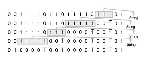
Table 5.4 Modified Booth recoding using the string property of numbers
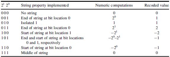
Example: This example multiplies two 8-bit signed numbers 10101101 and 10001101 using the Booth recoding algorithm. The technique first pairs the bits in the multiplier in 2-bit groups. Then, on checking the MSB of the previous group, it recodes each group using Table 5.4. A zero is assumed as MSB of the previous group for the least significant group as there is no previous group. The eight groups with the MSB of the previous group are:
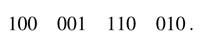
From the table the groups are recoded as –2, 1,-1 and 1, and the corresponding four PPs are generated as shown in Figure 5.47. For a 1 recoded digit in the multiplier, the multiplicand is simply copied. As each PP is generated for a pair of 2 bits of the multiplier, the i th PP is shifted by 2i places to the left. For the second recoded digit of the multiplier that is –1, the two’s complement of the multiplicand is copied. The PPs are generated for all the recoded digits; for the last digit of –2 the two’s complement of the PP is further shifted left by one bit position to cater for multiplication by 2. All the four PPs are sign extended and then added to get the final product. sig N -extension elimination logic can also be used to reduce the logic for HW implementation.
A representative HW design for implementing an 8 x 8-bit multiplier is given in Figure 5.48. The BR0, BR1, BR2 and BR3 recode by considering groups of 2 bits and the MSB of the previous group into one of the five recoded options. Based on the recoded value, one of the five PPs 2a, a,0,–a and –2a are generated. All the four PPs are then input to a compressor. The compression generates two layers of PPs that are then added using a CPA and a 16-bit product is computed.
Figure 5.47 Generation of four PPs
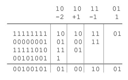
Figure 5.48 An 8 x 8-bit modified Booth recoder multiplier
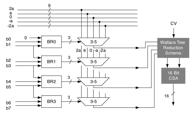
5.9.5 Modified Booth Recoded Multiplier in RTL Verilog
The example here implements a 6 x 6-bit MBR multiplier. The three components in the design are Booth recoder, CV generation and PPs accumulation. The design is implemented in Verilog and code is listed at the end of this chapter. A Verilog function RECODERfn implements the recoding part. It divides the 6 bits of the multiplier into three groups of 2 bits each. RECODERfn takes three bits as input, consisting of two bits of each group and the MSB of the previous group, and generates one of the five values 0,1, –1,2 or –2 as output. AVerilog task, GENERATE_PPtk, generates three PPs with sig N -extension elimination and a CV for the design. In cases where the recoded value is 2 or –2, the PP is generated by shifting the multiplicand or its compliment by 1 to the left, and this requires the PP to be 7 bits wide. For all other cases the seventh bit is the sign bit of the multiplicand. sig N -extension elimination logic is implemented. This requires flipping the MSB of the PP. For the cases of multiplication by – 1 or –2, two’s complement of the PP is computed by flipping all the bits and adding 1 to the LSB location. The addition of 1 is included in the CV, and the vector is appended by 2'b 01 for multiplication by –1 and 2'b 10 for multiplication by –2, as in this case the LSB is shifted by one bit position to the left. The output of the task is three PPs and six LSBs of the CV. The sig N -extension elimination logic for the three PP is precalculated. By adding all the sig N -extension elimination bits we get the five MSBs of the CV as 5'b01011 as shown in Figure 5.49.
The code below illustrates the implementation of Booth recoding and sig N -extension elimination logic in RTL Verilog. As the focus of the example is to illustrate the MBR technique, it simply adds all the PPs and the CV to compute the product. As the PPs and CV form four layers, for optimized implementation a carry save reduction tree should be used to reduce these four layers to two, and then two layers should be added using a fast CPA.
Figure 5.49 Pre-calculated part of the CV
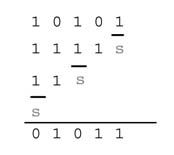
module BOOTH_MULTIPLIER (
 input [5:0] multiplier,
 input [5:0] multiplicand,
 output [10:0] product);
 parameter WIDTH = 6;

 reg [6:0] pps [0:2];
 reg [10:0] correction Vector;
 reg [2:0] recoderOut[2:0];
 wire [6:0] a, a_n;
 wire [6:0] _2a, _2a_n;
 //integer i;

 /*
 1 x multiplicand, sign extend the multiplicand, and flip the sign bit
 2 x multiplicand, shift a by 1 and flip the sign bit
 1 x multiplicand, sign extend multiplicand and then flip all bits except the
sign bit
 2 x multiplicand, shift a by 1, flip all the bits except the sign bit
 */
 assign a_n = {multiplicand[WIDTH-1], ~multiplicand};
 assign a = {~multiplicand[WIDTH-1], multiplicand};
 assign _2a_n = {multiplicand[WIDTH-1], ~multiplicand[WIDTH-2:0], 1’b0};
 assign _2a = {~multiplicand[WIDTH-1], multiplicand[WIDTH-2:0], 1’b0};
 // simply add all the PPs and CV, to complete the functionality
of the multiplier,
 // for optimized implementation, a reduction tree should be used
for compression
 assign product = pps[0] + {pps[1],2’b00} + {pps[2],4’b0000} +
correction Vector;
 always@*
 begin
 // compute booth recoded bits
 recoderOut[0] = RECODERfn ({multiplier[1:0],1’b0});
 recoderOut[1] = RECODERfn (multiplier[3:1]);
 recoderOut[2] = RECODERfn (multiplier[5:3]);
 // generate pps and correction vector
 GENERATE_PPtk (recoderOut[0], a, _2a, a_n, _2a_n, pps[0], correction Vector[1:0]);
 GENERATE_PPtk (recoderOut[1], a, _2a, a_n, _2a_n, pps[1], correction Vector[3:2]);
 GENERATE_PPtk (recoderOut[2], a, _2a, a_n, _2a_n, pps[2], correction Vector[5:4]);
 // pre-computed CV for sign extension elimination correction Vector[10:6] =5’b01011;
 //correction Vector[10:6] = 5’b00000;
end
/* ******************************************************
*task: GENERATE_PPtk
*input: multiplicand, multiplicand one’s complement
*recoderOut: output from bit-pair recoder
*output: correctionVector:addbitsfor2’scomplementcorrection
*output: ppi: ith partial product
 ******************************************************
 */
task GENERATE_PPtk;
input [2:0] recoderOut;
input [WIDTH:0] a;
input [WIDTH:0] _2a;
input [WIDTH:0] a_n;
input [WIDTH:0] _2a_n;
output [WIDTH:0] ppi;
output [1:0] correction Vector;
reg [WIDTH-1:0] zeros;
begin
 zeros = 0;
 case(recoderOut)
 3’b000:
 begin
 ppi ={1’b1,zeros};
 //ppi ={1’b0,zeros};
 correction Vector = 2’b00;
 end
 3’b001:
 begin
 ppi = a;
 correction Vector = 2’b00;
 end
 3’b010:
 begin
 ppi = _2a;
 correction Vector = 2’b00;
 end
 3’b110:
 begin
 ppi = _2a_n;
 correction Vector = 2’b10;
 //correction Vector = 2’b00;
 end
 3’b111:
 begin
 ppi = a_n;
 correction Vector = 2’b01;
 //correction Vector = 2’b00;
 end
 default:
 begin
 ppi =’bx;
 correction Vector = 2’bx;
 end
 endcase
 end
endtask
/* ******************************************************
*Function: RECODERfn
*input: one bit pair of multiplier with high order bit of previous pair, for
*first pair a zero is appended as previous bit
*output: Booth recoded output in radix-4 format, according to the following table
* ****************************************************** */
function [2:0] RECODERfn;
 input [2:0] recoderIn;
 begin
 case(recoderIn)
 3’b000: RECODERfn = 3’b000;
 3’b001: RECODERfn = 3’b001;
 3’b010: RECODERfn = 3’b001;
 3’b011: RECODERfn = 3’b010;
 3’b100: RECODERfn = 3’b110;
 3’b101: RECODERfn = 3’b111;
 3’b110: RECODERfn = 3’b111;
 3’b111: RECODERfn = 3’b000;
 default: RECODERfn = 3’bx;
 endcase
 end
 endfunction
endmodule
5.10 Compression Trees for Multi–operand Addition
Although several devices in the FPGA families offer embedded multipliers, compression trees are still critical in many applications. The compression tree is the first building block in reducing the requirement on the number of CPAs for multi-operand addition. This is explained here with the help of an example.
The example adds five signed operands in Q1.5, Q5.3, Q4.7 and Q6.6 formats. Different bits in each operand can be represented with dots and be aligned with respect to the place of the decimal in their respective Q-format. The sig N -extension logic is first constructed which is then eliminated by computing a correction vector and adding it as the sixth layer in dot representation. The placement of dots on a grid as shown in Figure 5.50 requires a compression tree to reduce the number of dots in each column to two. Any reduction technique can be used to demonstrate the effectiveness of the methodology. Here the Dadda reduction is employed. The two operands are then input to a CPA for final addition.
5.11 Algorithm Transformations for CSA
The CSA plays a key role in implementing high-throughput DSP applications in hardware. As a first step, while mapping a dataflow graph to architecture, the graph is observed to exhibit any potential use of CSAs and the graph is modified accordingly. For example, consider implementing the following equations:
Figure 5.50 Example illustrating use of a compression tree in multi-operand addition
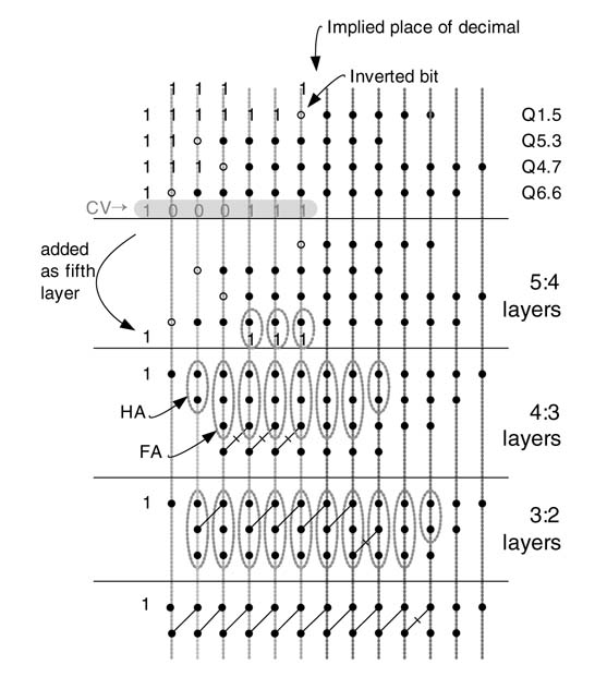
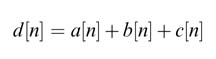
The equations are converted to the DFG of Figure 5.51(a). This is modified to use a CSA for compressing a [n] + b [n] + c [n] into two numbers, which then are added using a CPA. The transformed DFG is shown in Figure 5.51(b).
Figure 5.51 (a) FSFG with multi-operand addition. (b) Modified FSFG reducing three operands to two
This technique of extracting multi-operand addition can be extended to dataflow graphs where the graphs are observed to exhibit any potential use of CSA and compression trees. The graphs are then first transformed to optimally use the compression trees and then are mapped in HW. Such transformations are proven to significantly improve HW design of signal processing applications [13].
Multiple addition operations are the easiest of all the transformations. The compression tree can also be placed in the following add–compare–select operation:
To transform the logic for optimal use of a compression tree, the algorithm is modified as:
This compression tree transformation on the equivalent DFG is shown in Figure 5.52. Similarly the following add and multiply operation is represented with the equivalent DFG:
The DFG can be transformed to effectively use a compression tree. A direct implementation requires one CPA to perform op 2 + op 3, and the result of this operation is then multiplied by op1 . A multiplier architecture comprises a compression tree and a CPA. Thus to implement the computation two CPAs are required. A simple transformation uses the distributive property of the multiplication operator:
Figure 5.52 Compression tree replacement for an add compare and select operation
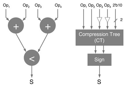
Figure 5.53 Transforming the add and multiply operation to use one CPA and a compression tree
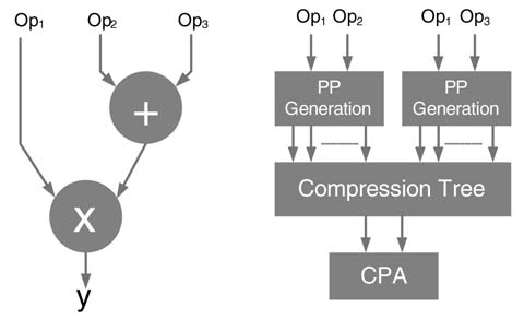
This representation of the expression now requires one compression tree that is then followed by one CPA to compute the final value. The associated DFG and the transformation are shown in Figure 5.53.
Extending the technique of generating partial sums and carries can optimize hardware implementation of a cascade of multiplications as well:
The transformation first generates PPs for op1 x op2 and reduces them to two PPs, s1 and c1:
These two PPs independently multiply with op 3, which generates two sets of PPs that are again reduced to two PPs, s 2 and c 2, using a compression tree:
These two PPs further multiply with op 4 to generate two sets of PPs that are again compressed to compute the final two PPs, s 3 and c 3. These two PPs are then added using a CPA to compute the final product:
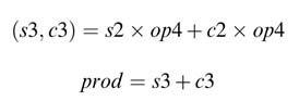
The equivalent transformation on a DFG is illustrated in Figure 5.54.
Following these examples, several transformations using basic mathematical properties can be used to accumulate several operators for effective use of compression trees for optimized hardware mapping.
Figure 5.54 Transformation to use compression trees and a single CPA to implement a cascade of multiplication operations
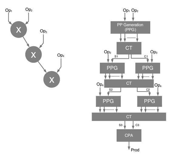
Exercises
Exercise 5.1
An eighth-order IIR filter is designed using the fdatool of MATLAB®. The four second-order parallel sections of the filter are given below. The coefficients of the first-order numerators are:
1 0.6902
1 –0.1325
1 1.7434
1 0.0852
The coefficients of the corresponding second-order denominator of the four second-order filters are:
1 –1.0375 0.7062
1 –0.6083 0.9605
1 –1.3740 0.5431
1 –0.7400 0.8610
Convert the coefficients in appropriate 16-bit fixed-point format. Code the design using FDA in RTL Verilog. Use mathematical operators for multiplication and addition in the code. Test your design for functional correctness. Synthesize your design of two families of FPGAs that support 18x18-bit multipliers and DSP48 blocks. Select the option in the synthesis tool to use these blocks. Compare your results for better timing and area.
Exercise 5.2
Design an 8-coefficient FIR filter and use a pipelined structure that optimally utilizes DSP48 blocks of Xilinx families of FPGAs. Write RTL Verilog code of the design. Synthesize the design with and without pipelining options to show the improvements.
Exercise 5.3
Perform appropriate mathematical transformation to effectively use compression trees to map the following equation:
Assume a,b,c,d and e are signed numbers in Q3.2, Q3.2, Q1.3, Q2.4 and Q1.3 formats, respectively. Use a Wallace reduction scheme for compression and draw the design logic in dot notation. Use the following numbers to verify the design:
Exercise 5.4
Design an optimal hardware to implement the following equation:
where a, b and c are in Q4.4, Q3.5 and Q2.6 format unsigned complex numbers, respectively. Verify your design for a =11.5 +j 4.23, b = 2.876 + j 1.23 and c=1.22 + j 3.32. First convert these numbers in specified Q format and then design the logic, showing compression trees as blocks in the design.
Exercise 5.5
Design a 32-bit hybrid adder that combines different adder blocks. Use 4-bit RCA, 8-bit CSA, 8-bit conditional sum adder, 8-bit Brent-Kung and 4-bit of carry look-ahead adders in cascade. Write RTL Verilog code of the design and synthesize your design on any Spartan™-3 family of FPGAs. Now design different 32-bit adders exclusively using the above techniques. Synthesize all the adders on the same FPGA and compare your results for area and timing.
Figure 5.55 Bit array for Dadda reduction
Exercise 5.6
Add the following two numbers using conditional sum addition techniques:
Exercise 5.7
Design and code in RTLVerilog a 16-bit conditional sum adder with two stages of pipeline (add one register to break the combinational cloud). Assume C_in is not known prior to addition.
Exercise 5.8
Multiply a 5-bit signed multiplicand a with a 5-bit unsigned multiplier b by applying a sig N -extension elimination technique, compute the correction vector for multiplication. Use the computed correction vector to multiply the following:
Exercise 5.9
Reduce the bit array shown in Figure 5.55 using a Dadda reduction scheme. Specify the number of FAs and HAs required to implement the scheme.
Exercise 5.10
Design and draw (using dot notation) an optimal logic to add twenty 1-bit numbers. Use a Dadda reduction tree for the compression.
Exercise 5.11
Design a single-stage pipelined 8x8 complex multiplier using modified Booth recoding for partial product generation and a (3,3:4) GPC reduction scheme for partial product reduction. Use minimum CPA in the design. Write RTL Verilog of the design and synthesize the design for a Spartan™-3 family of FPGAs. Compare your results with 3:2 and 4:2 compressor-based designs.
Exercise 5.12
Compute the correction vector for sign extension elimination for the following mathematical expression:
where x, y and z are Q1.3, Q2.3 and Q3.3 signed numbers, respectively. Use the correction vector to evaluate the expression for x = 1011, y = 11011 and z = 101111. Give equivalent floating-point values for x, y, z and w .
Exercise 5.13
Compute the correction vector for sign extension elimination for computing the following equation:
where in1, in2, in3, in4, in5 and in6 are in Q3.5, Q7.8, Q1.6, Q8.2, Q2.4 and Q3.9 formats, respectively.
Exercise 5.14
Design and draw (using dot notation) an optimal logic to implement the following code:
if (a+b+c+d+e+f > 4)
 x=4;
elseif (2a+2b+c+d+e+2f > 0)
 x=6;
else
 x=0;
a , b , c , d , e and f are 6-bit signed numbers, x is a 4-bit register. Use a Wallace compression tree and minimum number of carry propagate adders (CPAs) to implement the design.
Exercise 5.15
Reduce the following equation using Wallace reduction tree, and count how many full adders and half adders are required to compute the expression in two layers:
with
Use dot notation to represent the bits of each number, and assume all numbers are signed. Also compute the correction vector to eliminate sig N -extension logic.
Exercise 5.16
Multiply the following two signed numbers using a modified Booth recoding technique:
References
1.Xilinx.Virtex-4 multi-platform FPGAs: www.xilinx.com/products/virtex4/index.htm
2.Xilinx.User guide: Virtex-5 FPGA Xtreme DSP Design Considerations.
3.H. T. Kung and R. P. Brent, “A regular layout for parallel adders,” IEEE Transactions on Computers , 1982, vol. 31, pp. 260–264.
4.T. Han and D. A. Carlson, “Fast area-efficient VLSI adders,” in Proceedings of 8th IEEE Symposium on Computer Arithmetic , 1987, pp. 49–56.
5.O. J. Bedriji, “Carry select adder,” IRE Transactions on Electronic Computers , 1962, vol. 11, pp. 340–346.
6.J. Sklansky, “Conditional-sum addition logic,” IRE Transactions on Electronic Computers , 1960, vol. 9, pp. 226–231.
7.W. Schardein, B. Weghaus, O. Maas, B. J. Hosticka and G. TriSster, “A technology-independent module generator for CLA adders,” in Proceedings of 18th European Solid State Circuits Conference , 1992, pp. 275–278, Copenhagen, Denmark.
8.V. Kantabutra, “A recursive carry look-ahead carry-select hybrid adder,” IEEE Transactions on Computers , 1993, vol. 42, pp. 1495–1499.
9.M. Lehman and N. Burla, “Skip techniques for high-speed carry propagation in binary arithmetic circuits,” IRE Transactions on Electronic Computers , 1961, vol. 10, pp. 691–698.
10.C. Nagendra, M. J. Irwin and R. M. Owens, “Area–time tradeoffs in parallel adders,” IEEE Transactions on Circuits and Systems-11 , 1996, vol. 43, pp. 689–702.
11.J.-G. Lee, J.-A. Lee and D.-Y. Lee, “Better area–time trade offs in an expanded design space of adder architecture by parameterizing bit-width of various carry propagated sub-adder-blocks,” Proceedings of 6th IEEE International Workshop on System-oN -Chip for Real-Time Applications , 2006, pp. 10–14.
12.Xilinx. DSP: Designing for Optimal Results – High-performance DSP using Virtex-4 FPGAs, 10th edn, 2005.
13.A.K. Verma, P. Brisk and P. Ienne, “Data-flow transformationsto maximize the use of carry-save representation in arithmetic circuits,” IEEE Transactions on Computer-Aided Design of Integrated Circuits and Systems , 2008, vol. 27, pp. 1761–1774.
14.J. Poldre and K. Tammemae, “Reconfigurable multiplier for Virtex FPGA family,” in Proceedings of International Workshop on Field-programmable Logic and Applications , Glasgow, 1999, pp. 359–364, Springer-Verlag, London, UK.
15.O. Kwon, K. Nowka and E. E. Swartzlander, “A 16-bit by 16-bit MAC design using fast 5:3 compressor cells,” Journal of VLSI Signal Procsesing , 2002, vol. 31, no. 2, pp. 77–89.
16.H. Parandeh-Afshar, P. Brisk and P. Ienne, “Efficient synthesis of compressor trees on FPGAs,” in proceedings of Asia and South Pacific Design Automation Conference , 2008, pp. 138–143, IEEE Computer Society Press, USA.
17.K. Satoh, J. Tada, K. Yamaguchi and Y. Tamura, “Complex multiplier suited for FPGA structure,” in Proceedings of 23rd International Conference on Circuits/Systems, Computers and Communications , 2008, pp. 341–344, IEICE Press, Japan.
18.H. Parandeh-Afshar, P. Brisk and P. Ienne, “Improving synthesis of compressor trees on FPGAs via integer linear programming,” Design, Automation and Test in Europe , 2008, pp. 1256–1261.
19.A.Avizienis, “Signed-digit number representation for fast parallel arithmetic,” IRE Transactions on Electronic Computers , 1961, vol. 10, pp. 389–400.
20.F. Xu, C. H. Chang and C. C. Jong, “Design of low-complexity FIR filters based on signed-powers-of-two coefficients with reusable common sub expressions,” IEEE Transactions on Computer Aided Design of Integrated Circuits and Systems , 2007, vol. 26, pp. 1898–1907.
21.S.-M. Kim, J.-G.Chung and K. K. Parhi, “Low-error fixed-width CSD multiplier with efficient sign extension,” IEEE Transactions on Circuits and Systems II , 2003, vol. 50, pp. 984–993.