
13
Digital Design of Communication Systems
13.1 Introduction
This chapter covers the methodology for designing a complex digital system, and an example of a communication transmitter is considered.
Major blocks of the transmitter are the source coding block for voice or data compression, forward error correction (FEC) for enabling error correction at the receiver, encryption for data security, multiplexing for adding multiple similar channels in the transmitted bit stream, scrambling to avoid runs of zeros or ones, first stage of modulation that packs multiple bits in a symbol and performing phase, frequency, amplitude or a hybrid of these modulations, and digital up-conversion (DUC) to translate a baseb and modulated signal to an intermediate frequency (IF). This digital signal at IF is passed to a digital-to-analog (D/A) converter and then forwarded to an analog front end (AFE) for processing and onward transmission in the air.
The receiver contains the same components, cascaded together in reverse order. The receiver first digitizes the IF signal received from its AFE using an A/D converter. It then sequentially passes the digital signal to a digital down-converter (DDC), demodulator, descrambler, demultiplexer, decryption, FEC decoder and source decoder blocks. All these blocks re-do whatever transformations are performed on the signal at the transmitter.
Receiver design, in general, is the more challenging because it has to counter the noise introduced on the signalon its way from the transmitter. Also, the receiver employs components that are running at its own clock, and frequency synthesizers that are independent of the transmitter clock, so this causes frequency, timing and phase synchronization issues. Multi-path fading also affects the received signal. All these factors create issues of carrier frequency and phase synchronization, and frame and symbol timing synchronization. The multi-path also adds inter-symbol interference.
For high data-rate communication systems most of the blocks are implemented in hardware (HW). The algorithms for synchronizations in the receiver require complexnested feedback loops.
The transmitter example in this chapter uses a component-based approach. This approach is also suitable for software-defined radios (SDRs) using reconfigurable field-programmable gate arrays (FPGAs) where precompiled components can be downloaded at runtime to configure the functionality.
Using techniques explained in earlier chapters, this chapter develops time-shared, dedicated and parallel architectures for different building blocks in a communication transmitter. MATLAB® code is listed for the design. A critical analysis is usually required for making major design decisions. The communication system design gives an excellent example to illustrate how different design options should be used for different parts of the algorithm for effective design.
A crucial step in designing a high-end digital system is the top-level architecture, so this chapter first gives design options and then covers each of the building blocks in detail. For different applications these blocks implement different algorithms. For example, the source encoding may compress voice, video or data. The chapter selects one algorithm out of many options, and gives architectural design options for that algorithm for illustration.
13.2 Top-Level Design Options
The advent of software-defined radios has increased the significance of top-level design. A high data-rate communication system usually consists of hybrid components comprising ASICs, FPGAs, DSPs and GPPs. Most of these elements are either programmable or reconfigurable at runtime. A signal processing application in general, and a digital communication application in particular, requires sequential processing of a stream of data where the data input to one block is processed and sent to the next block for further processing. The algorithm that runs in each block has different processing requirements.
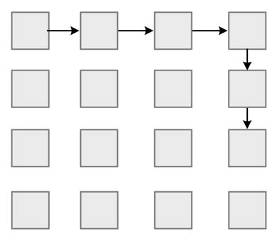
There are various design paradigms used to interconnect components. These are shown in Figure Figure 13.1.
13.2.1 Bus-based Design
In this design paradigm, all the components are connected to a shared bus. When there are many components and the design is complex, the system is mapped as a system-on-chip (SoC). These components are designed as processing elements (PEs). A shared bus-based design then connects all the PEs in an SoC to a single bus. The system usually performs poorly from the power consumption perspective. In this arrangement, each data transfer is broadcast. The long bus has a very high load
Figure 13.1 Interconnection configurations. (a) Shared bus-based design. (b) Peer-to-peer connections. (c) NoC-based design
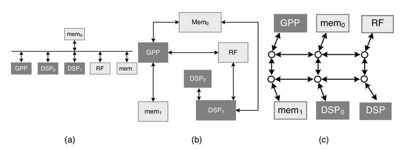
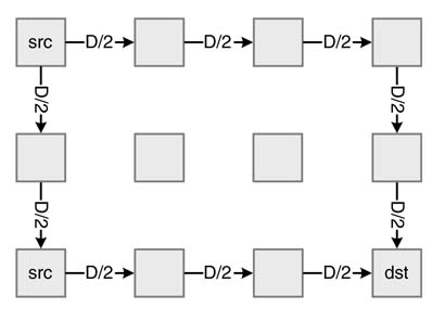
Figure 13.2 Split shared bus-based design for a complex digital system
capacitance C, and this results in high power dissipation as power is directly proportional to C as given by the formula:
where f and V are clock frequency and supply voltage, respectively.
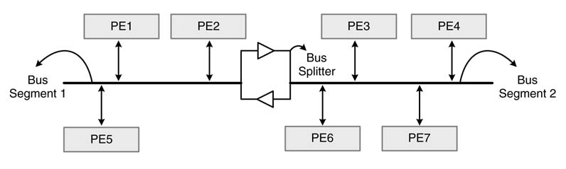
Segmenting the shared bus is commonly used to improve the performance. This segmentation also enables the bus to make parallel transfers in multiple segments. As the length of each segment is small, so is its power dissipation. A segmented bus design is shown in Figure 13.2.
Examples of on-chip shared-bus solutions are AMBA (advanced microcontroller bus architecture) by ARM [1], Silicon Backplane µNetwork by Sonics [2], Core Connect by IBM [3], and Wishbone [4].
A good example of a shared bus-based SoC is the IBM Cell processor. In this, an element interconnect bus (EIB) connects all the SPEs for internal communication. The bus provides four rings of connections for providing shared bandwidth to the attached computing resources [5].
Although designs based on a shared bus are very effective, they have an inherent limitation. Resources use the same bus, so bus accesses are granted using an arbitration mechanism. In network-on-chip (NoC) designs, parallel transfers of data among the PEs are possible. This flexibility comes at the cost of additional area and power dissipation.
13.2.2 Point-to-Point Design
In this design paradigm, all the components that need to communicate with each other are connected togetherusingdedicatedandexclusiveinterconnects.Thisobviously,for a complex design with many components, requires a large area for interconnection logic. In design instances with deterministic inter-PE communication, and especially for communication systems where data is sequentially processed and only two PEs are connected with each other, this design option is very attractive.
13.2.3 Network-based Design
Shrinking geometries reduce gate delays and their dynamic power dissipation, but the decreasing wire dimensions increase latency and long wires require repeaters. These repeaters consume more power. Power consumption is one of the issues with a shared bus-based design in SoC configuration. In a network-based architecture, all the components that need to communicate with other are connected to a network of interconnections. These interconnections require short wires, so this configuration helps in reducing the power dissipation along with other performance improvements (e.g. throughput), as multiple parallel data transfers are now possible. The network is intelligent and routes the data from any source to any destination in single or multiple hops of data transfers. This design paradigm is called network-on-chip.
An NoC-based design also easily accommodates multiple asynchronous clocked components. The solution is also scalable as the number of cores on the SoC can be added using the same NoC design.
13.2.4 Hybrid Connectivity
In a hybrid design, a mix of three architectures can be used for interconnections. A shared bus-based architecture is a good choice for applications that rely heavily on broadcast and multicast. Similarly, point-to-point architecture best suits streaming applications where the data passes through a sequence of PEs. NoC-based interconnections best suit applications where any-to-any communication among PEs is required. A good design instance for the NoC-based paradigmis a platform with multiple programmable homogenous PEs that can execute a host of applications. A multiple-processor SoC is also called an MPSoC. In MPSoC, some of the building blocks are shared memories and external interfaces. The Cisco Systems CRS-1 router is a good example; it uses 188 extensible network processors per packet processing chip.
A hybrid of these three settings can be used in a single device. The connections are made based on the application mapped on the PEs on the platform.
13.2.5 Point-to-Point KPN-based Top-level Design
A KPN-based architecture for top-level design is a good choice for mapping a digital communication system. This is discussed in detail in Chapter 4.
Figure 13.3 lays out a design. Without any loss of generality, this assumes all PEs are either microprogrammed state machine based architecture or time-shared architecture and run at asynchronous independent clocks, or a global clock where input to the system may be at the A/D converter sampling clock and the interface at the out put of the system then works at the D/A converter clock. A communication system is usually a multi-rate system. A KPN-based design synchronizes these multi-rate blocks using FIFOs between every two blocks.
13.2.6 KPN with Shared Bus and DMA Controller
A direct memory access (DMA) is used to communicate with external memory and off-chip peripheral devices. The design is augmented with components to support on chip transfers. A representative top-level design is shown in Figure 13.4.
Figure 13.3 KPN-based system for streaming applications
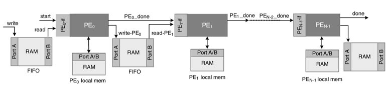
Figure 13.4 Shared-bus and KPN-based top-level design with DMA for memory transfers
All the PEs, program memories (PMs), data memories (DMs), general-purpose processor, peripherals and external memory interfaces and DMA are connected to a shared bus. The GPP acting as bus master configures the registers in the PEs and sets registers of DMA for bringing data into data memories and programs into program memories from external memory. The PEs also set DMA to bring data from the peripherals to their local DMs. Using the shared bus, the DMA also transfers data from any local DM block to any other.
All PEs have configuration and control registers that are memory mapped on GPP address space. By writing appropriate bits in the control registers, the GPP first resets and then halts all PEs. It then sets the configuration registers for desired operations. The DMA has memory access to program memory of each PE. When there are tables of constants, then they are also DMA to data memories of specific PEs before a micro-program executes.
PEi, after completing the task assigned to it, sets the PEi_done flag. When the next processing on the data is to be done by an external DSP, ASIC, or any other PE on the same chip, the done signal is also sent to the respective CCi . of the PEi . This let the CCi to set a DMA channel for requisite data transfer. The DMA when gets the access to the shared bus for this channel of DMA it makes the data transfer between on-chip and off-chip resources. A PE can also set a DMA channel to make data transfers from its local data memory to the DM of any other PE.
A representative design of a DMA is shown in Figure 13.5. The DMA has multiple channels to serve all CCs. Each CCi is connected to DMA through the config_DMA field. This has several configuration-related bits such as CCi _ req . This signal is asserted to register a request to DMA by specifying source, destination and block size to configure a DMA channel. The controller of the DMA in a round-robin fashion processes these requests by copying the source, destination and block size to an empty DMA channel. The controller also, in a round-robin arrangement, copies a filled DMA channel to executea DMA channel for actual data transfer. To make the transfer, the DMA gets accesstothe shared bus and then makes the requisite transfer.After the DMAisdonewith processing the channel, the DMA assert CCi_req _done flag and also set the DMA channel free and starts processing the next request if there is any.
Figure 13.5 Multi-channel DMA design
13.2.7 Network-on-Chip Top-level Design
The NoC paradigm provides an effective and scalable solution to inter-processor communication in MPSoC designs [6, 7].In these designs the cores of PEs are embedded in an NoC fabric. The network topology and routing algorithms are the two main aspects of NoC designs. The cores of PEs may be homogenous (arranged in a regular grid connected to a grid of routers). In many application-specific designs, the PEs may not be homogenous, so they may or may not be connected in a regular grid. To connect the PEs a number of interconnection topologies are possible.
13.2.7.1 Topologies
Topology refers to the physical structure and connections of nodes in the network. This connectivity dictates the routing abilityof the design. Figure 13.6 gives some configurations. The final selection is based on the traffic pattern, the requirements of quality of service (QoS), and budgeted area and power for interconnection logic. For example, grid [8] and torus [6] arrangements of routers are shown in Figure 13.6(a) and Figure 13-6(b). In these, a router is connected to its nearest neighbors. Each router is also connected with a PE core that implements a specified functionality. This arrangement is best for homogenous PEs with almost uniform requirements on inter-processor communication, or a generic design that can be used for different applications. It also suits run-time reconfigurable architectures. The generic and flexible nets of routers enable any type of communication among the PEs.
Figure 13.6 Network-on-chip configurations: (a) grid; (b) torus; (c) binary tree; (d) irregular connectivity; (e) mixed topology
In many designs a physically homogenous network and regular tile shape of processing elements are not always possible. The PEs, owing to their varied complexity, may be of different sizes. Application-specific SoCs require different handling of configurations and routing algorithms [9]. To select optimal topologies for these SoCs, irregular structures are usually designed.
13.2.7.2 Switching Options
There are two switching options in NoC-based design: circuit switching and packet switching. The switching primarily deals with transportation of data from a source node to a destination node in a network setting. A virtual path in NoC traverses several intermediate switches while going from source to destination node.
In circuit switching, a dedicated path from source to destination is first established [10]. This requires configuration of intermediate switches to a setting that allows the connection. The switches are shared among the connected nodes but are dedicated to make the circuit-switched transmission possible. The data is then transmitted and, at the end, the shared resource is free to make another transmission.
In contrast, packet switching breaks the data into multiple packets. These are transported from source to destination. A routing scheme determines the route of each packet from one switch to another. A packet-based network design provides several powerful features to the communication infrastructure. It uses very well established protocols and methodologies in IP networks, to enable the nodes to perform unicast, multicast and QoS-based routing. Each PE is connected with a network interface (NI)to the NoC. This interface helps in seamless integration of any PE with the others on an SoC platform. The NI provides an abstraction to the IP cores for inter-processor communications. Each PE sends a request to the NI for transferring data to the destination PE. The NI then takes the data, divides it into packets, places appropriate headers, and passes each packet to the attached routers.
Store and Forward Switching
In this setting, router A first requests its next-hop router B for transmission of a packet. After receiving a grant, A sends the complete packet to B. After receiving the complete packet, B similarly transmits the packet to the next hop, and so on.
Virtual Cut-Through Switching
In this setting, a node does not wait for reception of a complete packet. Router A, while still receiving a packet, sends a request to the next-hop router B. After receiving a grant from B, A starts transmitting the part of the packet that it has already received, while still receiving the remainder from its source. To cover for contention, each node must have enough buffer to hold an entire packet of data.
Wormhole Switching
In wormhole switching, the packet is divided into small data units called ‘flits’. The first flit is the headflit and it contains the header information for the packet and for theflitstofollow. The data itself is divided into several body flits. The last flit is the tail flit.Figure 13.7 shows division of a packet into flits and a snapshot of their distribution in a number of switches in a path from source to destination. All routers operate on these smaller data units. In this switching the buffers are allocated for flits rather than for entire packets.
Figure 13.7 Wormhole switching that divides a packet into multiple flits. (a) Packet divided into flits. (b) Wormhole switching of flits
13.2.7.3 Routing Protocols
A router implements options out of a number of routing protocols. All these protocols minimize some measure of delays and packet drops. The delay may be in terms of the number of hops or overall latency. In a router on a typical NoC, a switch takes the packet from one of the inputs to the desired output port.
The system may perform source routing, in which the entire route from source to destination is already established and the information is placed in the packet header. Alternatively the system may implement routing where only the destination and source IDs are appended in the packet header. A router based on the destination ID routes the packets to the next hop. For a more involved design where the PEs are processing voice, video and data simultaneously, a QoS based routing policy may also be implemented that looks into the QoS bits in each received packet and then prioritizes processing of packets at each router. For the simplest designs, pre-scheduled routing may also be implemented. An optimal schedule for inter-processor communication can then be established.
Based on the schedule, the NoC can be optimized for minimum area and power implementation.
13.2.7.4 Routing Algorithms
For an NOC, a routing algorithm determines a path from a set of possible paths that can virtually connect a source node to a destination node. There are three types of routing algorithm: deterministic, oblivious and adaptive.
- The deterministic algorithm implements a predefined logic without any consideration of present network conditions [11–19]. This setting for a particular source and destination always selects the same path. This may cause load imbalance and thus affects the performance of the NoC. The routing algorithm is, however, very simple to implement in hardware.
- The oblivious algorithm adds a little flexibility to the routing options. A subset of all possible paths from source to destination is selected. The hardware selects a path from this subset in a way that it equally distributes the selection among all the paths. These algorithms do not take network conditions into account.
- The adaptive algorithm , while making a routing decision, takes into account the current network condition. The network condition includes the status of links and buffers and channel load condition. A routing decision at every hop can be made using a look-up table. An algorithm implanted as combinational logic may also makes the decision on the next hop.
Figure 13.8 XY routing
XY Routing
This is a very simple to design logic for routing a packet to the next hop. The address of the destination router is in terms of (x,y ) coordinates. A packet first moves in the x direction and then in the y direction to reach its destination, as depicted in Figure 13.8. For cases that result in no congestion, the transfer latency of this scheme is very low, but its packet throughput decreases sharply as the packet injection rate in the NoC increases. This routing is also deadlock free but results in an unbalanced load on different links.
Toggled XY Routing
This is from the class of oblivious schemes. It splits packets uniformly between XY and YX. If a packet is routed using YX, it first moves in the y direction and then in the xdirection. It is also very simple to implement and results in balanced loads for symmetric traffic. Figure 13.9 shows an NoC performing toggled XY routing by switching D/2 packetsin XYand the othersin YXwhile routing a uniform load of D packets.
Figure 13.9 Toggled XY routing
Weighted Toggled XY Routing
The weighted version of toggled XY routing works on a priori knowledge of traffic patterns among nodes of the NoC. The ratios of XY and YXare assigned to perform load balancing. Each router has a field that is set to assign the ratios. To handle out-of-sequence packet delivery, the packets for one set of source and destination are constrained to use the same path.
Source-Toggled XY Routing
In this routing arrangement, the nodes are alternately assigned XYand YXfor load balancing. Thescheme results in balance loads for symmetric traffic. This is shown in Figure 13.10
Deflection Routing
In this routing scheme, packets are normally delivered using predefined shortest-path logic. In cases where there is contention, with two packets arriving at a router needing to use the same path, the packet with the higher assigned priority gets the allocation and the other packet is deflected to a non-optimal path. Deflection routing helps in removing buffer requirements on the routers [20].
13.2.7.5 Flow Control
Each router in an NoC is equipped with buffers. These buffers have finite capacity and the flow control has to be defined in a way that minimizes the size of the buffers while achieving the required performance. Each router has a defined throughput that specifies the number of bits of data per second a link on the router transfers to its next hop. The throughput depends on the width of the link and clock rate on each wire. To minimize buffer sizes, each packet to be transferred is divided into a number of flits of fixed size.
The transfer can be implemented as circuit switching, as described in Section 13.2.7.2. This arrangement does not require any buffers in the routers, but the technique results in an overhead for allocation and de-allocation of links for each transfer.
Figure 13.10 Source-toggled XY routing
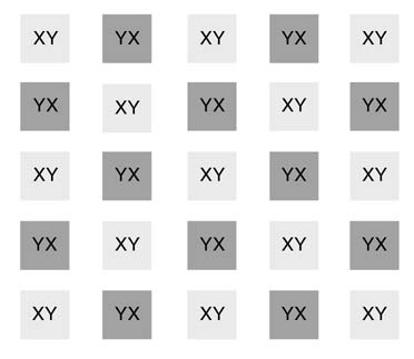
Figure 13.11 Flow control. (a) One channel per link. (b) Multiple virtual channels per link
Packet switching is a more effective for flow control. This requires a buffer on each outgoing or incoming link of each router. For routers supporting wormhole switching, the unit of transfer is a flit. Flits that are competing for the same link are stored in a buffer and wait for their turn for transfer to the next hop.
13.2.7.6 Virtual Channels
For buffer-based flow control, each link of a router is equipped with one buffer to hold a number of flits of the current transfer. A link with one buffer is shown in Figure 13.11.(a) If the packet is blocked at some node, its associated flits remain in buffers at different nodes. This results in blockage of all the links in the path for other transfers. To mitigate this blocking, each link can be equipped with multiple parallel buffers, and these are called ‘virtual channels’ (VCs). A link with three virtual channels is shown in Figure 13.11(b).
The addition of virtual channels in NoC architecture provides flexibility but also adds complexity and additional area. Switching schemes have been proposed that use VCs for better throughput and performance [21–23].
13.2.8 Design of a Router for NoC
A representative design of a router in an NoC infrastructure is given in Figure 13.12 [24]. The router assumes connectivity with its four neighbors and with the PE through a network interface. This connectivity consists of five physical channels (PCs) of each router. To provide more flexibility and better performance, a PC is further equipped with four virtual channels (VCs). A packet of data is written in the FIFO queue of the NI. The packet is broken into a number of flits. The packet transmission undergoes VC allocation, flit scheduling and switch arbitration. A packet is broken into a head flit followed by a number of data flits and ends with a tail flit. The header flit has the source and destination information. The fliterizing and VC assignment is performed at the source PE, and reassembly of all the flits into the original packet is done at the destination PE. An association is also established with all the routers from source to destination to ensure the availability of the same VC on them. This one-to-one association eases the routing of the body flits through the route. Only when this VC to VC association is established is the packet assigned a VC identification (VCid). The process of breaking a packet into flits and assigning a VCid to each flit is given in Figure 13.13.
Figure 13.12 Design of a router with multiple VCs for each physical channel
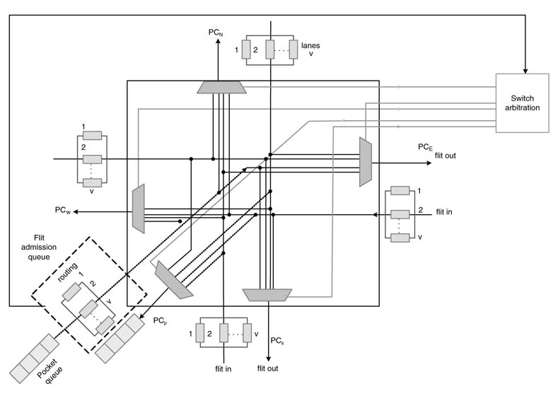
At the arrival of a header flit, the router runs a routing algorithm to determine the output PC on which the switch needs to route this packet for final destination. Then the VC allocator allocates the assigned VC for the flit on the input PC of the router.
Figure 13.13 Process of breaking a packet into a number of flits and assigning a VCid to each
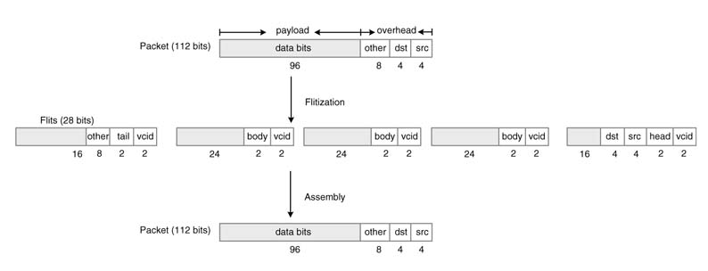
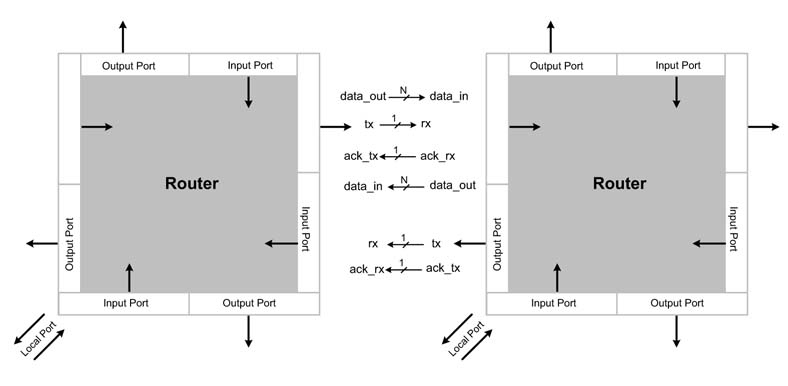
Figure 13.14 Design of an interface between two adjacent routers
Credit-based flow control is used for coordinating packet delivery between switches. The credits are passed across switches to keep track of the status of VCs. There are two levels of arbitration. First, out of many VCs on an input PC, only one is selected to use the physical link. At the second level, out of multiple sets of VCs from multiple input VCs connected to the output PC, one is selected to use the shared physical resource. A flit selected after these two arbitrations is switched out on the VC to the next router. Each body flit passes through the same set of VCs in each router. After the tail flit is switched out from a router, the VC allocated for the packet is released for further use.
A simple handshaking mechanism can be used for transmitting a flit of data on the PC [25]. The transmit-router places the flit on the data-out bus and a t x signal is asserted. The receive-router latches the flit in a buffer and asserts the ack-t x signal to acknowledge the transfer. Several of these interfaces are provided on each router to provide parallel bidirectional transfers on all the links. Figure 13.14 shows interfacing details of the links between two adjacent routers.
13.2.9 Run-time Reconfiguration
Many modern digital communication applications need reconfigurability at protocol level. This requires the same device to perform run-time reconfiguration of the logic to implement an altogether different wireless communication standard. The device may need to support run-time reconfigurability to implement standards for a universal mobile telecommunications system (UMTS) or a wireless local area network (WLAN). The device switches to the most suitable technology if more than one of these wireless signals are present at one location. If a mobile wireless terminal moves to a region where the selected technology fades away, it seamlessly switches to the second best available technology.
Although one design option is to support all technologies in one device, that makes the cost of the system prohibitively high. The system may also dissipate more power. In these circumstances it is better to design a low-power and flexible enough run-time reconfigurable hardware that can adapt to implement different standards. The design needs to be a hybrid to support all types of computing requirements. The design should have digital signal processors (DSPs), general-purpose processors (GPPs) and reconfigurable cores, accelerators and PEs. All the computing devices need to be embedded in the NoC grid for flexible inter-processor communication.
13.2.10 NoC for Software-defined Radio
An SDR involves multiple waveforms. A waveform is an executable application that implements one of the standards or proprietary wireless protocols. Each waveform consists of a number of components. These components are connected through interfaces with other components. There are standards to provide the requisite abstraction to SDR development. Software communication architecture (SCA) is a standard that uses an ‘object request broker’ (ORB) feature of common object request broker architecture (CORBA) to provide the abstraction for inter-component communication [26]. The components in the design may be mapped on different types of hardware resources running different operating systems. The development of ORB functionality in HW is ongoing, the idea being to provide a level of abstraction in the middleware that relieves the developer from low-evel issues of inter-component communication. This requires coding the interfaces in an interface definition language (IDL). The interfaces are then compiled for the specific platform.
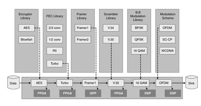
Figure 13.15(a) shows a library of components developed for waveform creation. Most of them have been developed for mapping in HW or SW platforms. The interfaces of these components are written in an IDL. While crafting a waveform, the user needs to specify the hardware resource on which a component is to be mapped. The HW resource may be a GPP, a DSP, an ASIC or an IP core. This hardware mapping of components on target technologies is shown in Figure 13.15.(b)
The component library lists several developed components for source encoding, FEC, encryption, scrambling, framing and modulation. The designer is provided with a platform to select resources from the library of components and connect them with other components to create a waveform. The designer also specifies the target technologies. In the example, the 16-QAM OFDM modulation is mapped on the DSP, whereas encryption and FEC are mapped on FPGA. The framer is mapped on a GPP.
Figure 13.15 Component-based SDR design. (a) Component library. (b) Waveform creaction and mapping on different target technologies in the system
The FPGA for many streaming applications implements MPSoC-based architecture. The components that are mapped on FPGA are already developed. An ideal SDR framework generates all the interfaces and makes an executable waveform mapped on a hybrid platform.
In the case of an SCA (software communications architecture) there may be CORBA-compliant and non-CORBA-compliant components in the design. ACORBA-compliant resource runs ORB as a middleware and provides an abstraction for inter-component communication among CORBA-compliant resources.
13.3 Typical Digital Communication System
A digital communication system is shown in Figure 13.16. A digital transmitter primarily consists of a cascade of sub-systems. Each sub-system performs a different set of computations on an input stream of data. Most of the blocks in the system are optional. Depending on the application, a transmitter may not source encode or encrypt data. Similarly the system may not multiplexdata from different users in a single stream for onward transmission. The system at the receiver usually has the same set of blocks but in reverse order. As the receiver needs to correct impairment introduced by the environment and electronic components, its design is more complex. In mobile/ cellular applications a base station or an access point may be simultaneously communicating with more than one end terminal, so it does a lot more processing than individual mobile end terminals.
13.3.1 Source Encoding
The input stream consists of digital data or a real-time digitized voice, image or video. The raw data is usually compressed to remove redundancy. The data, image and video processing algorithms are regular in structure and can be implemented in hardware, whereas the voice compression algorithms are irregular and are usually performed on a DSP.
For lossless data compression, LZW or LZ77 standard techniques are used for source encoding. These algorithms for high data rates are ideally mapped in HW. The images are compressed using the JPEG-2000 algorithm. This is also an ideal candidate for HW mapping for high-resolution and high speed applications. Similarly for video, a MPEG-4 type algorithm is used. Here, motion estimation is computationally the most intensive part of the algorithm and can be accelerated using digital techniques. Low bit rate voice compression, on the other hand, uses CELP-type algorithms. These have to compute LPC coefficients followed by vector quantization. The quantization uses an adaptive and fixed code book for encoding. These algorithms are computation- and code-intensive and are better mapped in software on DSPs.
13.3.2 Data Compression
As a representative component for source encoding, lossless data compression algorithms and representative architectures are discussed in this section.
LZ77 is a standard data compression algorithm that is widely used in many applications [27]. The compression technique is used also to preserve bandwidth while transmitting data on wireless or wired channels. An interesting application is in computer networks where, before data for each session is ported to the network, it is compressed at the source and then decompressed at the destination.
Figure 13.16 Representative communication system based on digital technologies
Figure 13.17 Sliding window for data compression algorithm
The algorithm works by identifying the longest repeated string in a buffer of data in a window. The string is coded with its earlier location in the window. The algorithm works on a sliding window. The window has two parts, a history buffer and a search buffer, with sizes N and M characters, respectively (Figure 13.17.)
The encoder finds the longest match of a string of character in a search buffer into the entire sliding window and codes the string by appending the last unmatched character with the backward pointer to the matched string and its length. The decoder then can easily decode by looking at the pointer and the last unmatched character. Figure 13.18 and the following code explain the working of the algorithm.
while (search buffer not empty)
 {
  find_longest_match() ! (position, length);
  code_match() ! (position, length, next unmatched character);
  shift left the window by length +1 characters;
}
Figure 13.18 Looking for the longest match
Figure 13.19 Parallel comparisons of characters listed in the first row with the three characters in the search buffer
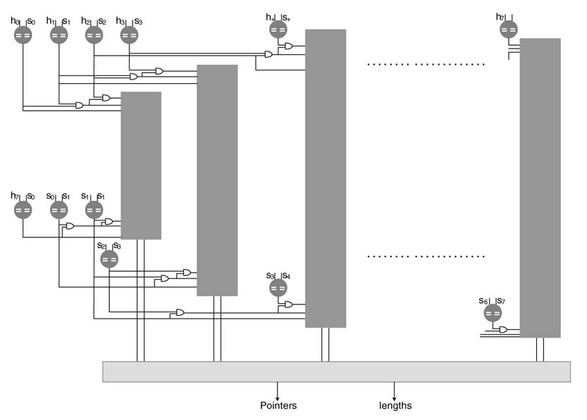
The compression algorithm is sequential, so an iteration depends on the result of the previous iteration. It might appear that a single iteration of the algorithm can be parallelized, but multiple iterations are difficult to parallelize. A technique can be used where the architecture computes all possible results for the subsequent iterations and then finally makes the selection. This technique is effective to design high-speed architectures for applications that have dependencies across iterations. An implementation of the technique to design a massively parallel architecture to perform LZ77 compression at a multi-gigabit rate is presented in [28–30]. A representative architecture is given in this section.
Here the example assumes a history buffer h of size 8 and maximum match of 3 characters that requires a search buffer s of size 3. The architecture performs all the matches in parallel. These matches are shown in the grid of Figure 13.19. The first row shows the values of the history and search buffers that are compared in parallel with the three characters in the search buffer.
The architecture computes the longest match of the search buffer [s0 s1 s2] to the string of characters listed in the first row. When it finds a match it computes the length of the match and also identifies its location. The size of history and the search buffers offer a tradeoff between area and achievable compression ratio, because the larger the buffer the larger the area.
Figure 13.20(a) computes the best match for one iteration of the algorithm. Each row computes a comparison listed in arrow of the grid of Figure 13.19. Each comparator compares the two characters and generates 1 if there is a match. A cascaded AND operation in each row carries forward the 1 for successive matches. The output of the AND operation is also used in each column to select the row that results in a successful match. The serial logic is a column is shown in Figure 13.21(a). The logic ORs the results of all rows in each column, and the last row of multiplexers selects the length of the maximum match and the multiplexer pointer_muxselects the pointer.
Beside serial realization of the column logic, the logic can be optimized for logarithmic time. The optimized logic groups the serial logic to work in pairs and is depicted in Figure 13.21(b). This results in that identifies the location of the match logarithmic rather than serial complexity.
Architecture can be designed that computes multiple iterations of the algorithm. The architecture is optimized as computations are shared across multiple iterations. Figure 13.22 displays a table showing all the possible comparisons required for performing multiple iterations of the algorithm, highlighting the sharing of comparisons in the first three columns.
The first column of the table shows the first iteration. The second column computes the result if no match is established in the first iteration, and s0 is moved from the search buffer to the history buffer with coding (0 0 s0). Similarly the third, fourth and fifth columns show if the first iteration results in match length of 1, 2 and 3, respectively. If the first iteration matches two characters, than columns 4, 5 and 6 are considered for the next iteration. If all three characters are matched, then columns 5 and 6 are considered for the next iteration. If no match is found, the architecture implements sixiterations of the algorithm in parallel. The table also highlights the sharing that is performed across iterations.
Figure 13.20 Digital design for computing iteration of the LZ77 algorithm in parallel. (a) Identifying logic in each column. (b) A block representing the logic of three columns and pointer and length calculation
Figure 13.23 shows the architecture that implements these multiple iterations. The selection block finally selects the appropriate answer based on the results of the multiple iterations.
13.3.3 Encryption
The encryption block takes source encoded data as clear text and ciphers the text using a pre-stored key. AES is the algorithm of choice for most digital communication applications. The algorithm is very regular and designed for hardware mapping. A representative architecture for moderate data rate applications is described below.
13.3.3.1 AES Algorithm
An AES algorithm encrypts a 128-bit block of plain text using one of three sizes of key, 128, 192 or 256 [31]. The encryption is performed in multiple rounds. For the three key sizes the number of rounds for data encryption are n= 10, 12 and 14. In the key scheduling stage, the key is expanded to (4n + 4) number of 32-bit words. This operation is done once for an established key and can be performed offline to support multiple rounds of operation. The plain text is arranged into four 32-bit words in a state matrix. Most of the operations in the algorithm are performed on 32-bit data. These operations are ‘add round key’ (ARK), ‘byte substitution’ (BS), ‘shift rows’ (SR) and ‘mixcolumn’ (MC). A block diagram is shown in Figure 13.24.(a)
Figure 13.21 Pointer calculation logic for each column: (a) with serial complexity, and (b) with logarithmic complexity
Figure 13.22 Multiple iteration of the algorithm with shared comparisons
The flow of the algorithm is given in Figure 13.24.(b) The first step is filling of the state matrixwith 128 bits of plain text. The arrangement is shown in Figure 13.25, where the data is stored column wise. The first byte takes the first element of the first column.
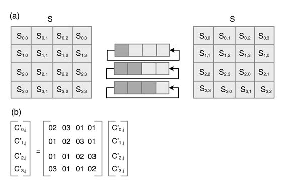
In the first operation of ARK, 128 bits of states are XO Red with 128 bits of the round key. The key is derived from the cipher key in the key scheduling stage. In the next operation of ARK, the 8-bit element of the state matrixis indexed in a pre-stored 256-entry table of S-boxand the entry is replaced by the entry in S-box. The substitution is followed by a shift row operation where the rows 0, 1, 2 and 3 are circularly rotated to the left by 0, 1, 2 and 3, respectively. The operation is shown in Figure 13.26(a). After shifting rows, the state matrixis trans formed in an MC operation. In this, each column of the state matrixin multiplied in GF (28) to the matrixgiven in Figure 13.26(b). The MC operation is performed in all rounds except the final round of the algorithm. Pseudo-code of the AES Implementation is given here:
Figure 13.23 Digital design implementing multiple iterations of the LZ77 algorithm
// Nb = 4
// Nr = 10, 12, 14 for 128, 192 and 256 bit AES
// Hard parameter, Nk=4,6,8 for 128, 192, 256 AES
// UWord8 and UWord32 are 8-bit and 32-bit unsigned numbers
UWord32 key[Nk];
UWord32 w[Nb*(Nr-1)]; /* Expended Key */
AES_encryption (
UWord8 plain_text[4*Nb],
UWord8 cipher_text[4*Nb],
UWord32 w[Nb*(Nr-1)]);
begin
  UWord8 state [4*Nb];
  state = Plain_text;
   ARK(state, w[0, Nb-1]);
for(round=1, round<=Nr-1, round++)
begin
  SB(state);
  SR(state);
  MC(state);
  ARK(state, w[round*Nb, (round+1)*Nb-1)]);
end
SB(state);
SR(state);
ARK(state, w[Nr*Nb, (Nr+1)*Nb-1)]);
end
Figure 13.24 AES algorithm. (a) Block diagram of encryption. (b) Flow of a lgorithm for encryption and decryption
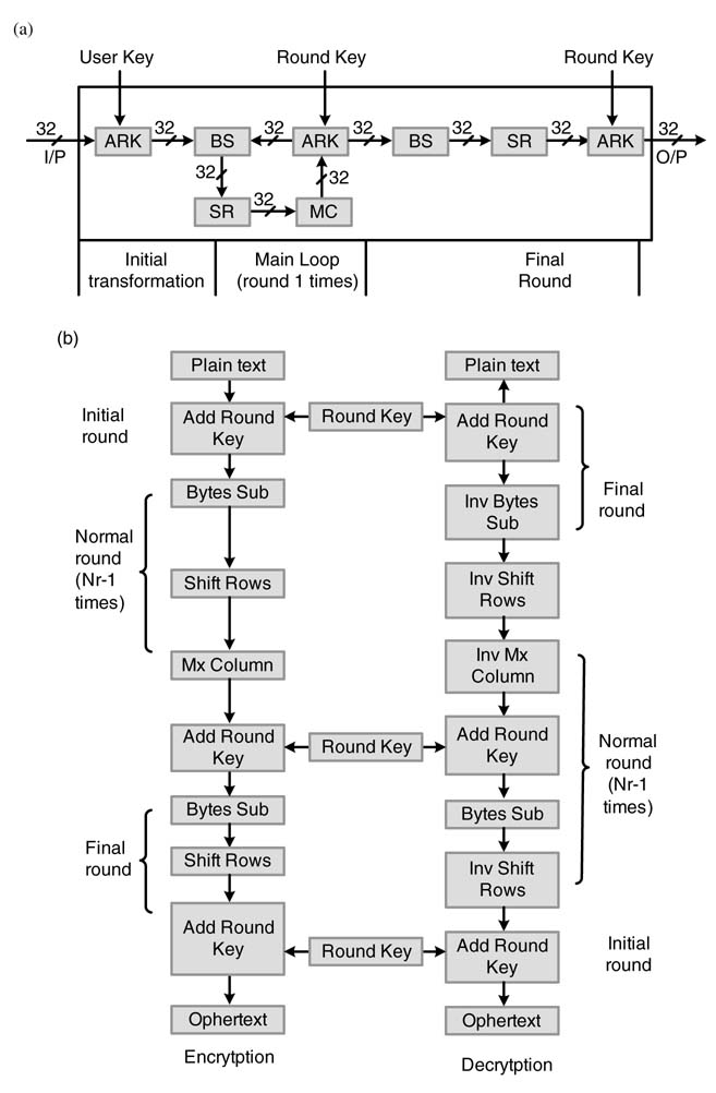
Figure 13.25 Filling of plain text in a state matrix
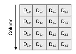
Figure 13.26 (a) Shift row operation of AES algorithm. (b) Matrixmultiplication of mixed column operation
13.3.3.2 AES Architectures
There are a number of architectures proposed in the literature. Selection of a particular implementation of the AES algorithm primarily depends on the input data rate. A pipelined fully parallel architecture implements all the iterations in parallel [35]. The design supports very high throughput rate and is shown in Figure 13.27(a). Similarly a design that uses time-shared architecture implements one round at a time. A representative layout is given in Figure 13.27(b).
There are many applications where the architecture is needed to support moderately high data rates in a small area, as is the case with most of the wireless communication standards. An optimal design may require further folding the AES algorithm from the one given in Figure 13.27(b). The design. though. is originally defined for 32-bit data units but can be broken into 8- or 16-bit data units [32, 33]. The HW mapping then reduces the requirement on buses, registers and memories from 32-bit to 8- or 16-bit while supporting the specified throughput. For an 8-bit design this amounts to almost four-fold reduction in hardware.
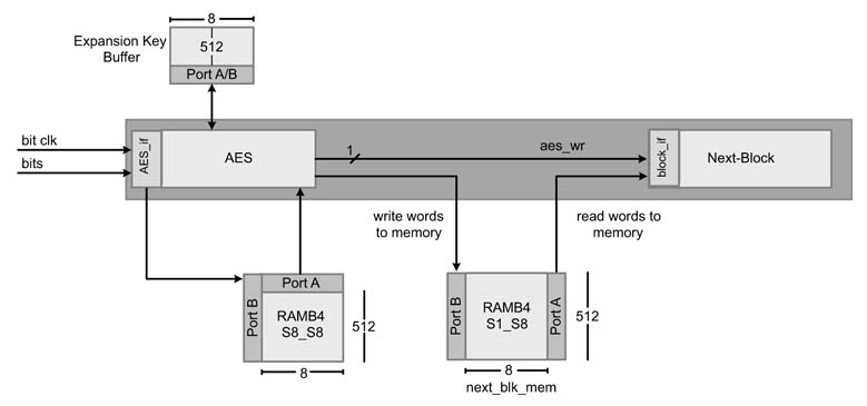
An example of an implementation of AES in a KPN network framework is shown in Figure 13.28. The AES processor reads plain text data from an input FIFO. The processor has an internal RAM that is used for local storage of temporary results. The cipher data is then stored into a FIFO and a done flag is set for the next block to start using the cipher data. The key once expended is stored in an internal RAM.
Figure 13.27 AES architectures. (a) Pipelined fully parallel design of AES. (b) Time-shared design
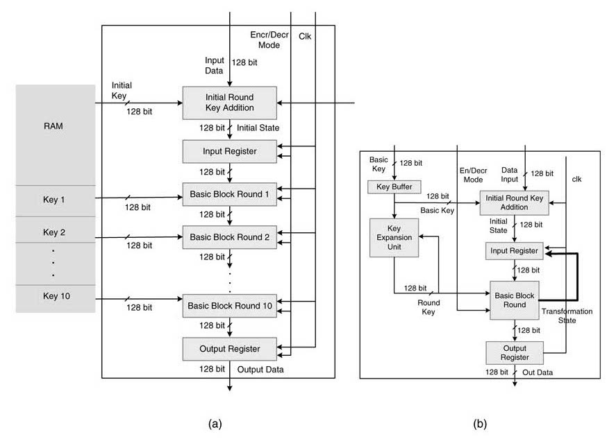
Figure 13.28 KPN-based top-level design incorporating an AES processor
The block diagram of the top-level design of the AES engine is given in Figure 13.29. Serial data is received to the engine at serial clock rate. The AES interface unit of the block accumulates the bits to make a 128-bit block and writes it to the AES input FIFO and generates a signal to the AES engine to start processing the data. The engine encrypts data and writes the result to the FIFO to the next block for onward processing.
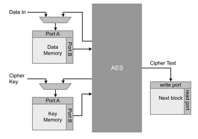
In a typical KPN configuration, an AES engine uses two instances of block RAM. One block also acts as a FIFO and data memory, the AES engine uses port B to read the data and port A to write the data back after each round in to the RAM. This port is also shared by the AES interfacetowriteanew128-bit of plain text into the RAM. The second RAM stores the cipher and the round keys. Although the design of AES can also perform key expansion with a little modification [32,33], only the ciphering is covered in this design. The engine writes the cipher text into the next block FIFO that is then read by the next processing block in the architecture. This memory configuration is given in Figure 13.30.
Figure 13.29 Top-level design of AES engine
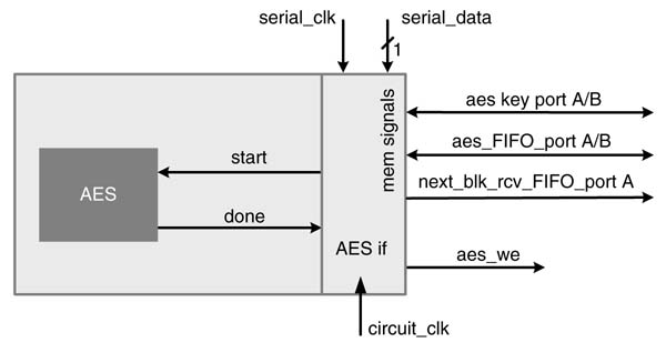
Figure 13.30 Memory configuration of AES engine in KPN settings
There are two types of memory in most of the FPGAs: distributed RAM and block RAM. The LUTs can be configured as distributed RAM whereas block RAM is a dedicated dual-port memory. An FPGA contains several of these blocks. For example, XC3S5000 in the Spartan-3 family of devices has 104 blocks of RAM totaling 1872 kilobits of memory. Similarly the LUT of a CLB in the Spartan-3 family can be optionally used as 16-deep ×1-bit synchronous RAM. These memories can be cascaded to form deeper and wider units. The distributed RAM should be used only for small memories as it consumes LUTs that are primarily meant for implementing digital logic. The block RAM should be used for large memories. Each block RAM is wrapped with a synchronous interface. The details on instantiating these two types of memory can be found from the user manual of a specific device [36, 37]. The memories and FIFOs are generated using the Xilinxcore generation tool. The top-level design using generated modules are given here.
module aes_top(
input clk,
input reset,
// Input interface
input [7:0]  wr_data_i,
input [3:0]  wr_data_addr_i,
input     wr_data_en_i,
input [7:0]  wr_key_i,
input [4:0]  wr_key_addr_i,
input     wr_key_en_i,
input     start_i,
input     rd_ff_data_en_i,
// Output interface
output [7:0]   rd_ff_data_empty,
// Use to indicate 128-bit in FIFO
output ff_data_avail_o//FIFO done
);
// Internal wires and regs
wire [7:0]  wr_data_int;
wire [3:0]  wr_data_addr_int;
wire      wr_data_en_int;
wire [7:0]  data_mux;
wire [3:0]   data_addr_mux ;
wire     data_wr_en_mux;
wire [7:0]   rd_data_int;
wire [3:0]  rd_data_addr_int;
wire [7:0]  rd_key_addr_int;
wire [3:0]  wr_ff_data_int;
wire [7:0]  wr_ff_data_e n_int;
wire      wr_ff_data_e n_int;
wire     wr_ff_data_full_int;
// Module instantiations
// Bus assignment
/* Initially the data is written in the data_mem from the
  external controller. When signal start_i is asserted
  the in-place AES encryption starts processing /
assign data_mux= (start_i) ? wr_data_int: wr_data_i;
assign data_addr_mux= (start_i) ? wr_data_addr_int: wr_data_addr_i;
assign data_wr_en_mux= (start_i) ? wr_data_en_int: wr_data_en_i;
// Input data memory: for holding 16 bytes, memory width of 8-bit
 input_data_mem input_data_mem_inst(
.clka   (clk),
.clkb   (clk),
.wea    (data_wr_en_mux), // Write interface
.addra   (data_addr_mux),
.dina   (data_mux),
.addrb   (rd_data_addr_int), // Read interface to AES
.doutb   (rd_data_int)
);
// Key sets
key_mem key_mem_inst(
.clka   (clk),
.clkb   (clk),
.wea    (wr_key_en_i), // Write interface
.addra   (wr_key_addr_i),
.dina   (wr_key_i),
.addrb   (rd_key_addr_int), // Read interface to AES engine
.doutb   (rd_key_int)
);
// AES engine
aes aes_inst(
.clk    (clk),
.reset  (reset),
// Write interface to input data memory for in-place computation
.wr_data_o   (wr_data_int),
.wr_data_addr_o   (wr_data_addr_int),
.wr_data_en_o   (wr_data_en_int),
// Read interface to input data memory
.rd_data_i      (rd_data_int),
.rd_data_addr_o   (rd_data_addr_int),
.rd_key_i      (rd_key_int), // Read interface to keys
.rd_key_addr_o    (rd_key_addr_int),
// Start signal from the external controller
.start_i ( start_i ),
// Write interface to data FIFO
.wr_ff_data_o    (wr_ff_data_int),
.wr_ff_data_en_o   (wr_ff_data_en_int),
.wr_ff_data_full   (wr_ff_data_full_int),
// Done and output written in FIFO
.ff_data_avail_o (ff_data_avail_o)
);
// Output data FIFO
output_ff output_ff_inst(
.rst    (reset),
.wr_clk  (clk),
.rd_clk  (clk),
.din    (wr_ff_data_int ), // Write interface
.wr_en   (wr_ff_data_en_int),
.full   (wr_ff_data_full_int),
// Read interface for extranl controller
.dout   (rd_ff_data_o),
.rd_en   (rd_ff_data_en_i),
.empty   (rd_ff_data_empty)
);
endmodule
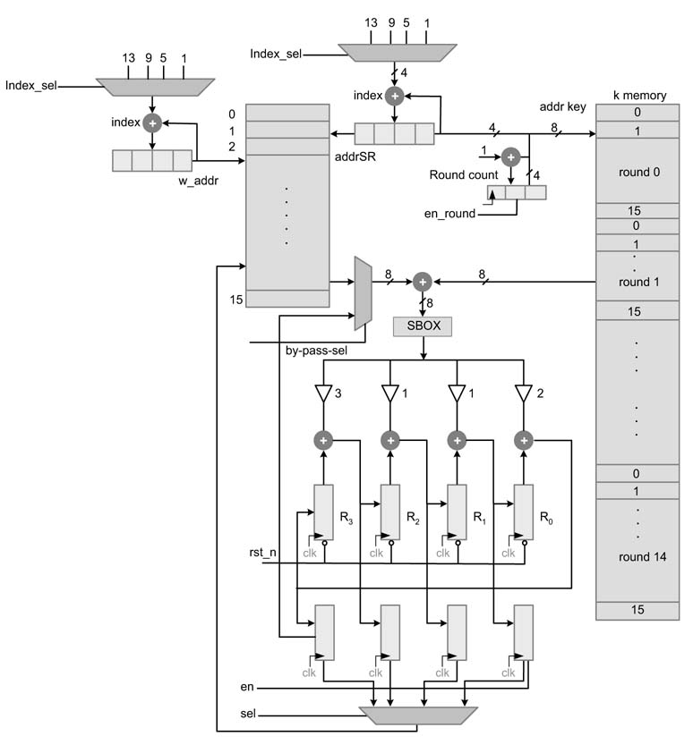
13.3.3.3 Time-Shared 8-bit Folding Architecture
There is no straightforward method of further folding AES architecture as the algorithm is iterative and nonlinear while it performs computation for a round. The standard folding techniques covered in Chapter 8 cannot be directly applied. A trace scheduling technique is used in [32, 33, 38]. In this technique all the flow of parallel computations in the algorithm are traced. The interdependencies across these traces are established. All these traces are then folded while taking account of their interdependencies and then are mapped in hardware.
The processor is designed to use 8-bit data. The architecture implements a 256 AES that requires 14 rounds. The processor uses an 8 ×240-bit memory for storing cipher and round key. The memory is managed as i=0, 1, 2,…, 14 sections for 15 ARK operations of the algorithm. Each section i stores 16 bytes (128-bit) of key for the i th iteration of the algorithm. The ARK block reads corresponding bytes of the key and the state in each cycle and XORs them. The data is read from memories in shift-row format, so logic for the SR operation is not required. The block BS is performed as reading from SBOXROM.
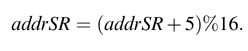
Figure 13.31 State indexing for shift-row operation: (a) original indexing, and (b) shift-row indexing
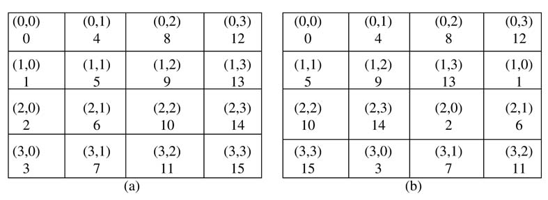
The technique maps the algorithm on to a byte-systolic architecture. Each iteration of the implementation reads an 8-bit state directly in row-shifted order. The original indexing of the states is shown in Figure 13.31(a) and the row-shifted indices are shown in Figure 13.31(b). To access the values of the states shown column-wise, a simple circular addressing mode is used.
The incremented SR indexis generated by implementing a modulo accumulator:
The %16 is implemented by a 4-bit free-running accumulator that ignores overflows. The same address is used to indexthe round key from key memory. A 4-bit counter roundCount is appended to the address to identify the round:
where addrKey is the address to the key memory. The design works on reading 8-bit data from the memory and ciphering the plain text in multiple iterations. Each round of AES requires 16 cycles of 8-bit operations. The design of ARK, SR and BS for 8-bit architecture is shown in Figure 13.32.
The 8-bit result computed from BS is then passed to the mix-column block. The 8-bit design works on a byte by byte input value from the BS block. The design multiplies each byte with four constant values in GF(28) as defined in the standard. The values in the constant matrixare such that each row has the same values just shifted by one to the right. This multiplication for the first column is shown here:
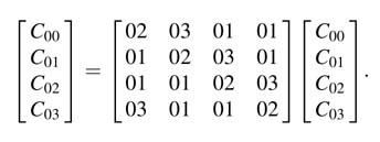
Figure 13.32 Eight-bit time-shared AES architecture
This arrangement helps in implementing the mix-column operation in byte-systolic manner. The architecture of the MC block is shown in Figure 13.33. The results of multiplication and addition are saved in registers shifted to the right by one. In the first cycle, C00 is input to the MC module and the output values of the computation are in the registers and the four registers have the
Figure 13.33 Mix-column design for byte systolic operation
following values:
In the next cycle the second byte of states C01 is used to compute the next term in the partial sums. At the end of the second cycle the registers have the following values:
Similarly in third cycle the following values are computed and stored in the registers:
And finally the fourth cycle computes a complete column and the values are latched in shadow registers:
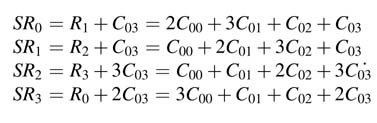
For in-place computation, these values from the shadow registers are moved into the locations of byte-addressable memory that are used to calculate these values. This requires generating indexvalues in a particular pattern. The logic that generates addressing patterns for in-place computation is explained in the next section. The MC module multiplies all the columns and saves the values in the data memory.
The first row of registers are also reset every fourth cycle for computing the multiplication of the next column. An enable signal latches the values of the final result in the second row of shadow registers. These values are then saved in the data memory by in-place addressing. As the same HW block is time-shared for performing the next round of the AES algorithm, the SR requires reading the fifteenth value in the fourth cycle for the MC computation in the next round. The value is still in the register of MC in this clock cycle. The value is directly passed for ARK computation. The timing diagram of Figure 13.34 illustrates the generation of different signals.
It is important to appreciate that in many applications no established technique can be applied to design an effective architecture. The 8-bit AES architecture described in this section is a good example that demonstrates this assertion. The algorithm is explored by expending all the computations in an iteration. Then, intelligently, all dependencies are resolved by tracing out single-byte operations to make the algorithm work on a single byte of input.
13.3.3.4 Byte-Systolic Fully Parallel Architecture
This section presents a novel byte-systolic fully parallel AES architecture [38]. The architecture works on byte in-place indexing. A byte of plain text is input to the architecture and a byte of cipher text is output in every clock cycle after an initial latency of 16 ×15 cycles. All the rounds of encryption are implemented by cascading all the stages with pipeline logic. The data is input to the first stage in byte-serial fashion. When the 16 bytes have been written in the first data RAM block, the stage starts executing the first round of the algorithm. At the same time the input data for the second frame is written in the RAM block by employing byte in-place addressing. This scheme writes the input data at locations that are already used in the current cycle of the design. For example, the first stage reads the RAM in row-shifted order reading indices 0, 5,10 and 15 in the first four cycles. The four bytes of input data for the second frame are written at these locations in the first RAM block.
The four tables in first row of Figure 13.35 show the write addresses for the first four frames in the first RAM block for data. These address patterns repeat after every four frames. The memory locations are given column-wise. The memory location is numbered in the corner of each box, while the indices of the values written in these locations are in the center. The four tables in the second row show the sequential ordering of these indices for reading in row-shifted order. The column-wise numbers show the memory locations that are read in a sequence to input the data in the specified format.
Figure 13.36 shows the systolic architecture. Each stage has its own RAM blocks for storing data for a round and corresponding key. The addressing for reading from the RAM block and writing the data in the same location is performed using the address generation unit shown with each memory block. The addressing is done using an index. For four successive frames the value of the indexis generated by adding 4 into the previous index. For writing into all the RAM blocks, the indexis initialized to 1. So the first write in each RAM block is in sequential order.
Figure 13.34 Timing diagram for the time-shared AES architecture
Figure 13.35 Byte in-place indexing for byte systolic AES architecture. (a) Indices for writing data for first four frames. (b) Memory locations for reading data in shift-row format
Figure 13.36 Byte systolic architecture implementing AES algorithm
For reading the data written in the RAM and at the same time writing the second frame on a byte by byte basis, the address is incremented as:
It is clear from Figure 13.36 that in-place storing of data into memory as given in (a) and then reading in data in row-shifted form for the second frame requires. The indexis updated after every 16 cycles as
This pattern is repeated every four frames. The indexvalue repeats as 1, 5, 9, and 13 and can be directly selected from a 4:1 MUXas shown in Figure 13.36. The last value (i.e. the fifteenth) computed for each round is directly sent to ARK of the next block for avoiding pipeline stall. The architecture perfectly works in lock step. Once all the pipeline stages are filled, each clock cycle inputs one byte of plain text data and generates one byte of ciphered output.
13.3.4 Channel Coding
In many communication systems, the next block in a transmitter is channel coding. This is performed at the transmitter to automatically correct errors at the receiver. The transmitter performs coding of the input data using convolution, Reed-Solomon or turbo codes. In many applications more than one type of error-correction coding is also performed. All these algorithms can be mapped in HW for high-throughput applications. Description and architecture design of an encoder for block turbo code (BTC) is given in this section.
The BTC serially combines two linear block codes, C1 and C2, to form the product code P =C1×C2 [39]. A block code is represented by (n,k), where n and k stand for code word length and number of information bits, respectively. For example, consider (7,4) extended Hamming code. This code takes four information bits, computes three parity bits and appends them to the information bits to create seven bits of code word. This can be represented by IIIIPPP , where I and P represent information and parity bits. A two-dimensional turbo code is constructed by successively applying coding to a 2-D information matrixfirst for all the rows and then for all the columns.
Figure 13.37 shows application of block turbo coding (7,4) by (7,4) to produce (49,16) block turbo code. The information is arranged in a 4 × 4 matrix. Each row of the matrix is block coded and three parity bits PH are attached. This operation results in a 4 × 7 matrix. Now each column of this matrixis again coded and the resultant matrixis shown in the figure.
A configurable design of a BTC encoder can be incorporated in a communication system that supports a wide range of code rates. For example, by appropriately selecting from n1,n2= 11,26,57 the block size of information matrixcan range from 121 bits to 4096 bits. For these values a number of options are available to the user, as given in Table 13.1. The 11 × 11 block of input data is coded as a 16 × 16 block where each row and column has 4 bits of c data and 1 bit of parity.
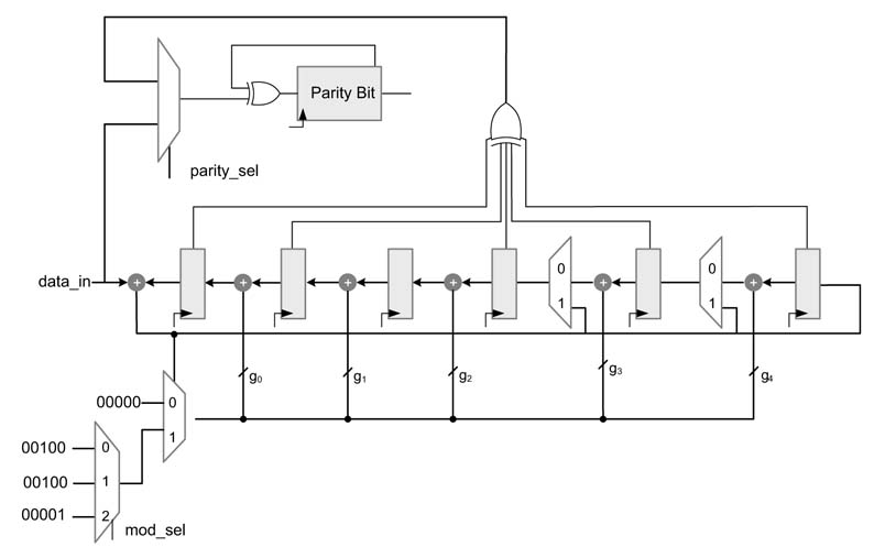
The standard Hamming encoder used for row and column operations is shown in Figure 13.38. The registers ri for i=0,…, 5 compute the redundant bits, where as rp computes the parity bit. The encoding polynomial is selected according to the code rate selected for encoding. Some of the registers are not used for low code rates. The mode-sel selects one of the modes of operation.
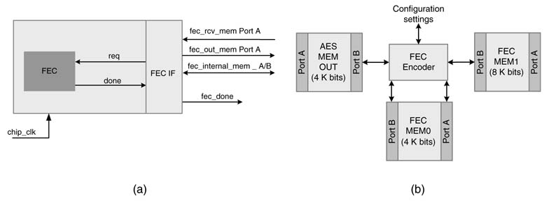
The BTC is best suited to be implemented in hardware in a typical KPN setting of Figure 13.3. This setting assumes three dual-port memories with an interface to the data path. Figure 13.39 shows the interfaces and the memory blocks. The BTC starts encoding the data once enough bits are available in AES out-memory which is filled by the AES engine of Section 13.3.3. The size is easily calculated using the read and write pointers of the FIFO controller of AES out-memory. The BTC reads the input data and keeps the intermediate results in its internal memory, and finally the output is written to BTC out-memory.
Figure 13.37 (49,16) block turbo code formulation by combining (7,4) x(7,4) codes
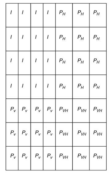
Table 13.1 Options for block turbo code for supporting different code rates
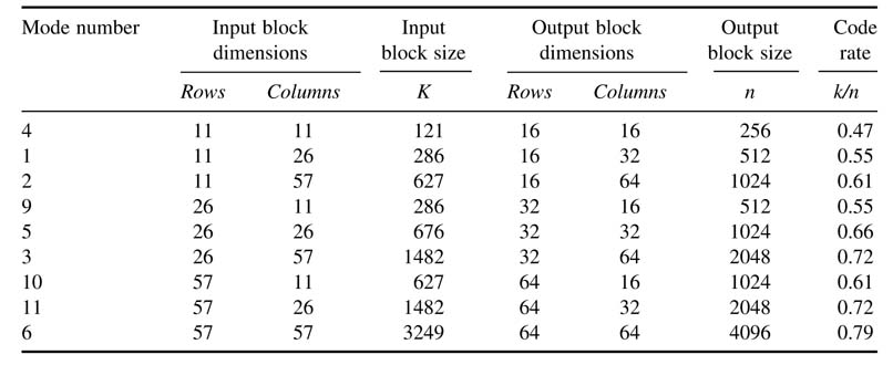
Figure 13.38 Standard Hamming encoder for BTC
The FEC engine reads data written by the AES engine in AES out-memory to perform horizontal encoding. The encoded datais written back into internal memory of the FEC engine. For the vertical coding, the data is read from the internal FEC memory and the encoded data is written into FEC out-memory.
13.3.5 Framing
For synchronization, different delimiters are inserted in data. For example, to indentify and synchronize an AES frame, an 8-bit AES header can be inserted after every defined number of AES buffers. Similarly, for synchronizing an FEC block, a header may also be inserted for synchronization. Beside these headers, in mobile communications a framer serves several purposes. It is used for synchronization of data at the receiver. In burst communication, it is used for detection of the start of a burst. A framer puts a pattern of bits as frame header that is also used for channel estimation, timing and frequency error estimation. Figure 13.40 shows insertion of headers for AES and FEC synchronization and a start of burst (SoB) header for burst detection and timing, frequency and channel estimation.
Figure 13.39 BTC system-level design. (a) BTC interfaces. (b) BTC memory block settings
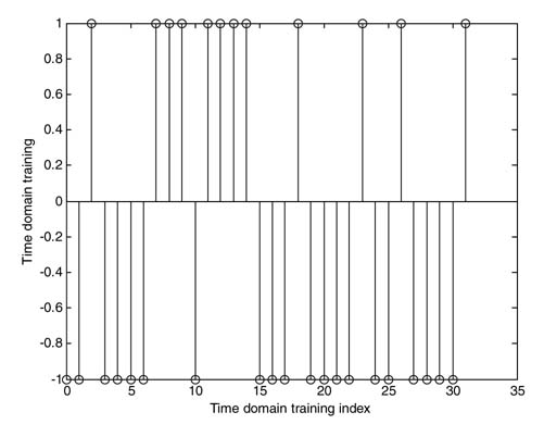
A training symbol can be designed to aid the estimation and synchronization process. The training symbol also acts as SoB [40–42]. The technique presented in [42] is especially designed to give good estimation of timing and frequency offsets and also provides ways of estimating channel impulse response. The method presented is generic and can be used for any type of single or multi carrier modulation scheme. A Golay complementary sequence C of length NG is selected and, for time-domain training, set A =C; for frequency-domain training assign A =fft(C). Now A is repeated L times with some sign pattern to generate a training sequence. The time-domain training sequence for L =4 shown in Figure 13.41.
The MATLAB® code below lists an implementation of the generation of these training sequences, from [42], for different values of L. The sequence is directly modulated for computing estimates and corrections at the receiver. For example, while performing OFDM modulation, the frequency-domain training sequence for a specific value of L can be generated offline and modulated with a carrier and appended with the OFDM modulated frames.
if L==2
 Sign_Pattern = [1 1];
 C = [1 1 -1 1 1 1 1 -1 1 1 -1 1 -1 -1 -1 1];
elseif L == 4
 Sign_Pattern = [-1 1 -1 -1];
 C = [1 1 -1 1 1 1 1 -1];
elseif L == 8
 Sign_Pattern = [1 1 -1 -1 1 -1 -1 -1];
 C = [1 1 -1 1];
elseif L == 16
 Sign_Pattern = [1 -1 -1 1 1 1 -1 -1 1 -1 1 1 -1 1 -1 -1];
 C = [1 1];
end
A = fft(C);
SoB_training = [];
for i=1:L
 SoB_training = [SoB_training Sign_Pattern(i)*A];
end
The sequence can be easily incorporated in the transmitted signal by storing it in a ROM and appending it with the baseband modulated signal.
13.3.6 Modulation
13.3.6.1 Digital Baseband Modulation
Modulation is performed next in a digital communication system. A host of modulation techniques are available, which may be linear or nonlinear. They may use single or multiple carriers. They may also perform time-, frequency- or code-division multiplexing for multiple users. A description of one of these techniques is given below.
Figure 13.40 Header and frame insertion for synchronization
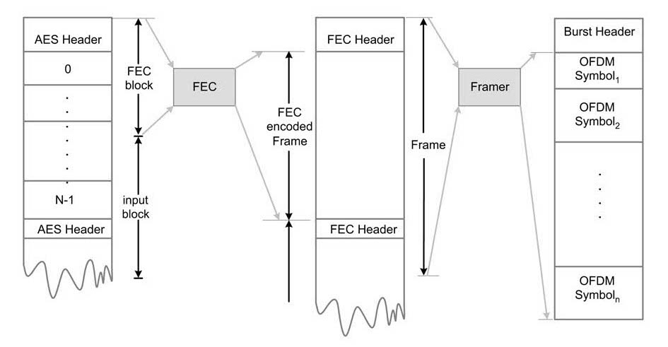
Figure 13.41 Time-domain training sequence
13.3.6.2 OFDM-based Digital Transmitter and Receiver
Owing to its robustness for multiple path fading, OFDM (orthogonal frequency-division multiplexing) is very effective for high-rate mobile wireless terminals. The scheme is used in many modern communication system standards for wireless networks, such as IEEE 802.11(a) and 802.16(a), and digital broadcasting such as DAB, DVB-T and DRAM. OFDM uses multiple orthogonal carriers for multi-carrier digital modulation. The technique uses complex exponentials. This helps in formulating the modulation as computation of an inverse Fast Fourier Transform (IFFT) of a set of parallel symbols, whereas FFT is performed at the receiver to extract the OFDM-modulated symbols:
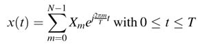
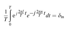
where Xm is the symbolto betransmitted on the subcarrier with carrier frequency fm = m /T . There are N multi-carriers in an OFDM system, and the subcarriers

are orthogonal to each other over interval [0, T ] as
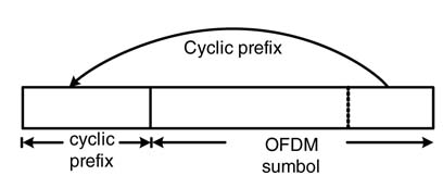
where l,n=01,2,…,N—1.At the transmitter, the bits are first mapped to symbol Xm, and N of these symbols (for m=0,…, N—1) are placed in parallel for IFFT computation. The output of IFFT is then serially modulated by a carrier frequency. To avoid inter symbol interference, and keeping the periodicity of the IFFT block intact, a cyclic prefix from the end of the IFFT block is copied to the start. The addition of a cyclic prefix is shown in Figure 13.42.
Figure 13.42 Adding cyclic prefix to an OFDM symbol
An OFDM system needs to address several issues that are standard to a communication system. These issues are carrier and sampling clock frequency offsets, OFDM symbol or frame offset, dealing with channel effects, and analog component noise and imperfections.
As the computation of timing and frequency offsets and the channel estimation are very critical for OFDM-based systems, some of the IFFT carriers may also be used as pilot tones. Training-based techniques are also popular that use a training sequence for these estimations. The MATLAB® code below shows the use of a training sequence for estimation and a 32-point IFFT-based OFDM transmitter. In the code the raw data is generated. The data is then block coded using a Reed-Solomon encoder. This encoding is followed by convolution encoding using a 2/3 encoder. The coded data is then mapped to QPSK symbols. These symbols are then grouped in parallel for OFDM coding:
clear a11
close a11
fec_en = 1;


% Each data set consists of 2 sets of 24 8-bit raw symbols,
% thus making the data length equal to 2*8*24=384
ofdm_burst_size = 24; % Number of OFDM frames in a burst of Tx
ofdm_train_per_burst = 1; % Number of trainings per burst
bps = 2;
DATA_SET_LEN = 384;
NO_OF_DATA_SET = 4; % For simulation


% RS code parameters adds 8 extra 8-bit symbols for error correction
RS_CODE_m = 8;
RS_CODE_k = 24;
RS_CODE_n = 32;


% After Reed–Solomn coding, the length of the burst becomes 2*8*32=512
% Convolution code parameters, the length becomes 512*3/2=768
% punct_code = [1 1 0 1];
code_rate = 1/2; %2/3;
trellis = poly2trellis(7, [133 171]);
tb_length = 3;
const_map = [-1-j -1+j 1-j 1+j];
N = 32; % dft_size
K = 4; % cyclic prefix


% OFDM symbol size with cyclic Prefix
sym_size = N + K;
L = 4; % for training
M = N/L;
% TRANSMITTER
% Generate raw data
raw_data = randint(1, DATA_SET_LEN*NO_OF_DATA_SET);
frame_out = [];
out = [];
un_coded = [];
for burst_index=0:NO_OF_DATA_SET-1
% process data on frame by frame basis
frame = raw_data(DATA_SET_LEN*burst_index+1:
 DATA_SET_LEN*(burst_index+1));
if (fec_en)
 % Block encoding
 % Put the raw data for RS encoder format
 % The encoder generates n m-bit code symbols, that has k m-bit message
 % symbols
 % First put the bits in groups of m-bits to convert them
 % to RS symbols
 msg_in = reshape(frame,RS_CODE_m,DATA_SET_LEN/RS_CODE_m)’;
 % Convert the m-bit symbols from binary to decimal while % considering the left bit as MSB msg_sm = bi2de(msg_in,’left-msb’);
 % Put the data in k m-bit message symbols
 rs_msg_sm = reshape(msg_sm,length(msg_sm)/RS_CODE_k,RS_CODE_k);
 % Convert the symbols into GF of 2^RS_CODE_m msg_tx= gf(rs_msg_sm, RS_CODE_m);
 % Encode using RS (n,k) encoder
 code = rsenc(msg_tx, RS_CODE_n, RS_CODE_k);
  % Convolution encoding
  tx_rs = code.x.’;
  tx_rs_st = tx_rs(:);
  bin_str = de2bi(tx_rs_st,RS_CODE_m,’left-msb’)’;
  bin_str_st = bin_str(:);
  un_coded = [un_coded bin_str_st’];
  % Perform convolution encoding
  % conv_enc_out = convenc(bin_str_st, trellis, punct_code);
   frame = convenc(bin_str_st, trellis)’;
end
   frame_out = [frame_out frame];
end
% QPSK modulation
out_symb =reshape(frame_out, bps, length(frame_out)/bps)’;
out_symb_dec = bi2de(out_symb,’left-msb’);
mod_out = const_map(out_symb_dec+1);
% OFDM modulation ofdm_mod_out = [];
% Generate OFDM symbols for one burst of transmission for index=0:ofdm_burst_size-1,
ifft_in = mod_out(index*N+1:(index+1)*N);
 ifft_out = ifft(ifft_in, N);
 ifft_out_cp = [ifft_out(end-K+1:end) ifft_out];
 ofdm_mod_out=[ofdm_mod_out ifft_out_cp];
end
A burst is formed that appends a training sequence of Figure 13.41 to the OFDM data. A number of OFDM symbols are sent in a burst. This number depends on the coherent bandwidth of the channel that ensures the flatness of the channel on the entire bandwidth of transmission. The training is used to estimate different parameters at the receiver:
% Generating training for start of burst, synchronization and estimation
% Generate the training offline and store in memory for
% appending it with input data
C = [1 1 -1 1 1 1 1 -1];
A = fft(C);
Sign_Pattern = [-1 1 -1 -1];
G = [];
for i=1:L
 G = [G Sign_Pattern(i)*A];
 end
% Add cyclic prefixto G
train_sym = [G(end-K+1:end) G]/4;
% Appending training to start of burst
ofdm_mod_out = [train_sym ofdm_mod_out];
The signal is transmitted after it is up-converted and mixed with a carrier. In a non-line-of-sight mobile environment the transmitted signal gets to the receiver through multiple paths. If there is a relative velocity between transmitter and receiver, the received signal frequency also experiences Doppler shift. The multi-path effects cause frequency fading. The signal also suffers from timing and frequency offsets. The channel impurities are modeled using a Rayleigh fading channel where timing and frequency offsets are also added to test the effectiveness of estimation and recovery techniques in the receiver. An additive white Gaussian noise (AWGN) is also added in the signal to test the design for varying signal to noise ratios (SNRs):
% Multi-path fading frequency selective channel model
ts = 1/(186.176e3); % sample time of the input signal
fd = 5; % maximum Doppler shift in Hz
tau = [0 8e-6 15e-6]; % path delays
pdb = [0 -10 -20]; % avg path gain
theta = 0.156; % frequency offset
SNR = 5; & signal to noise ratio in dbs
timing_offset = 18;
chan = rayleighchan(ts,fd,tau,pdb);
chan.StoreHistory = 1; % To plot the time varying channel
% Frequency selective multi-path fading channel
% Passing the signal through a multipath Rayleigh fading channel
% and adding other channel impurities
Received_Signal = filter(chan, ofdm_mod_out);
% Plot(chan)
Received_Signal = Received_Signal.*
 exp(j*2*pi*(theta/N)*(0:length(Received_Signal)-1));
Received_Signal = awgn(Received_Signal, SNR,’measured’);
Received_Signal = [zeros(1,timing_offset) Received_Signal];
The coarse timing estimation is based on correlation of the training signal that consists of L parts ofM size sequence. The algorithm computes the peak of the timing matrix given by the following set of equations:
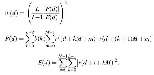
The MATLAB® code here implements these equations.
% RECEIVER
% Timing and frequency estimation
for k = 1:L-1
b(k) = Sign_Pattern(k)*Sign_Pattern(k+1);
end
% Timing estimation
for d=1:N
 E(d)= sum(abs(Received_Signal(d:d+L*M-1)).^2);
 P(d) = 0;
 for k=0:L-2
  index= d+k*M;
  indexP1= d+(k+1)*M;
  P(d) =P(d) + (b(k+1) * Received_Signal(indexP1:
   indexP1+M-1)*Received_Signal(index:index+M-1)’);
 end
 Timing_Metric(d) = ((L/(L-1))*abs(P(d))/E(d))^2;
end
[xy] =max(Timing_Metric);
Coarse_Timing_Point = round(y);
d_max= Coarse_Timing_Point;
For the frequency estimation, the training signal is first modified such that all the L parts have the same sign. This modified training symbol is represented by {y(k): k= 0,…, N — 1}.The coarse estimate is given by:
The following MATLAB® code implements these equations and computes frequency offset estimation:
% Frequency estimation
H = L/2;
H = L/2;
w(1)=0; % not used
for m = 1:H
  w(m+1)=3*L/(2*pi)*((L-m)*(L-m+1)-H*(L-H))/(H*(4*H^2-6*L*H+3*L^2-1));
end
y =[];
for i=1:L
  y =[y Sign_Pattern(i)*Received_Signal(d_max+M*(i-1):d_max+i*M-1)];
end
 for m = 0:H
 index= m*M;
 Ry(m+1) =1/(N-index) * y(index+1:N)*y(1:N-index)’;
 arg(m+1) =angle(Ry(m+1));
end
phi(1)=0; % not used
for m = 2:H+1
  phi(m) =arg(m)-arg(m-1);
  if phi(m) > pi
 phi(m) = phi(m) - 2*pi;
elseif phi(m) < -pi
 phi(m) = phi(m) + 2*pi;
 end
end
Coarse_Frequency = phi*w’
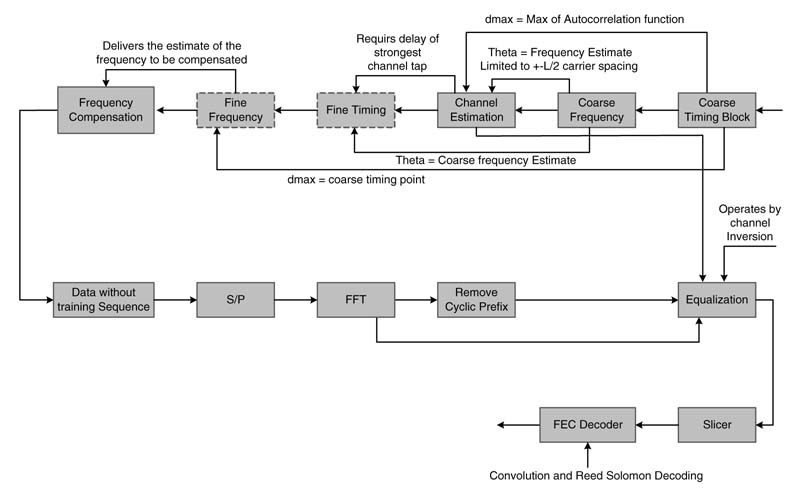
These coarse estimates are further refined in [42] and the block diagram of the system is shown in Figure 13.43.
The training signal also aids in estimating the channel impulse response. The channel is assumed to be static for a few OFDM symbols. If gains of K paths are:
Figure 13.43 Block diagram of complete OFDM receiver
then the received signal can be written as:
where
Here, {s(k): k=–Ng, –Ng+1,…, N—1} are the samples of the training sequence with cyclic prefix, n is the noise vector, v is the frequency offset, and r is the received signal. The channel estimation using coarse frequency offset can be written as:
where v is the coarse frequency offset estimate. The following MATLAB® code implements the channel estimation:
ct = Coarse_Timing_Point;
cf = Coarse_Frequency;
r = Received_Signal(ct:ct+N-1);
for i = 1:N
 w(i) =exp(j*2*pi*cf*(i+K-1)/N);
end
W = diag(w);
 S = zeros(N, K);
 for i = 1:N
 S(i,:) = fliplr(train_sym(i+1:K+i));
end
h_cap = inv(S’*S)*S’*W’*r.’;
Channel_Estimate = h_cap;
The receiver first needs to estimate the frequency and timing offset. It also needs to estimate the channel impulse response. When the timing and frequency errors have been estimated, the receiver makes requisite corrections to the received signal using these estimations. The channel estimation is also used to equalize the received signal. The OFDM, because of its multiple carriers, assumes the channel for each carrier as flat. This flat fading factor is calculated for each carrier and the output is adjusted accordingly. The symbols are extracted by converted output of FFT computation to serial and applying slicer logic to the output. The symbols are then mapped to bits:
% Frequency and timing offsets compensation
Received_Signal = Received_Signal(Coarse_Timing_Point-K:end);
Received_Signal =Received_Signal.* exp(-j*2*pi *
   ((Coarse_Frequency)/N)*(0:length(Received_Signal)-1));
Initial_Point = K+N+K+1;
Received_Signal = Received_Signal(Initial_Point:Initial_Point+(N+K) *
  (ofdm_burst_size-1)-1);
% Processing the synchronized data
Received_Signal = reshape(Received_Signal, N+K,ofdm_burst_size-1);
% Serial to parallel
Received_Signal_WOGI = Received_Signal(1:N,:); % remove cyclic prefix
Received_Signal_WOGI = fft(Received_Signal_WOGI,[],1);
Received_Signal_WOZP = zeros(N,ofdm_burst_size-1);
Received_Signal_WOZP(1:N/2,:) = Received_Signal_WOGI(1:N/2,:);
Received_Signal_WOZP((N/2)+1:end,:) = Received_Signal_WOGI(end-(N/2)+1:
end,:);
% Estimation
H = fft(Channel_Estimate,N);
CH = zeros(N,1);
CH(1:N/2) =H(1:N/2);
CH((N/2)+1:end) = H(end-(N/2)+1:end);
H_l_hat_square = abs(CH);
W = 1./CH;
% Equalization
Estimated_Signal= [];
for Symbol_Number = 1:1:ofdm_burst_size-1
Present_Symbol= Received_Signal_WOZP(:,Symbol_Number);
Estimated_Symbol = Present_Symbol.*W;
Estimated_Signal = [Estimated_Signal Estimated_Symbol]; end Received_Signal_WZP = reshape(Estimated_Signal, 1, N *
  (ofdm_burst_size-1)); % Parallel to serial % Scatterplot(Received_Signal_WZP) % Title(Equalizer Output’) Recovered_Signal= Received_Signal_WZP; % Received_Signal_WZP = reshape(Estimated_Signal, 1, N*(ofdm_burst_size-1)); % Parallel to serial
% Slicer
 Bit_Counter = 1;
 Bits = zeros(1,length(Recovered_Signal)*bps);
for Symbol_Counter = 1:length(Recovered_Signal)
  % Slicer for decision making [Dist Decimal] = min(abs(const_map -
Recovered_Signal(Symbol_Counter)));
% Checking for mimimum Euclidean distance est = const_map(Decimal);
Bits(1,Bit_Counter:Bit_Counter+bps-1) = de2bi(Decimal-1,bps,
‘left-msb’); % Constellation Point to Bits Bit_Counter = Bit_Counter + bps; end
scatterplot(Recovered_Signal) title(‘Received Constellation’) grid
Data = bit_stream(1:N*(ofdm_burst_size-1)*bps); ErrorCount = sum((Data~=Bits))
scatterplot(Received_Signal_WZP); title(‘Received Constellation’); grid
store = ErrorCount/length(Data)
Figure 13.44 shows the constellation of QPSK-based OFDM receiver of this section for different channel conditions. For deep fades in the channel frequency resource, an OFDM-based system is augmented with error-correction codes and interleaving. The interleaving helps in spreading the consecutive bits in the input sequence to different locations in the transmitted signal.
It is quite evident from the MATLAB® code that simple FFT and IFFT cores can be used for mapping the OFDM Tx/Rxin hardware. The channel estimation should preferably be mapped on a programmable DSP. The timing error and frequency errors can also be calculated in hardware. The system needs to be thought of as a cascade of PEs implementing different parts of the algorithm. Depending on the data rates, the HW mapping may be fully parallel or time-shared.
13.3.7 Digital Up-conversion and Mixing
The modulated signal is to be digitally mixed with an intermediate frequency (IF) carrier. In a digital receiver one of the two frequencies, 70 MHz or 21.4 MHz, is commonly used. The digital carrier is generated adhering to the Nyquist sampling criterion. To digitally mix the baseband signal with the digitally generated carrier, the baseband signal is also up-converted to the same sampling rate as that of the IF carrier. A digital up-converter performs the conversion in multiple stages using polyphase decomposition. The designs of digital up- and down-converters using polyphase FIR and IIR filters are given in Chapter 8.
Figure 13.44 Constellationof QPSK-based OFDM received signal for different channel conditions and frequency offsets. (a) 40 dB SNR. (b) 40 dB SNR with 30 Hz Doppler shift. (c) 20 dB SNR with 5 Hz Doppler shift. (d) 10 dB SNR
In direct communication transmitter and receiver the in phase and quadrature components of a modulated signal are converted to analog at baseband. The signal is then mixed using one or multiple stages of quadrature mixing and finally the signal is transmitted after passing it through a power amplifier.
13.3.8 Front End of the Receiver
The receiver front end usually performs processing in the analog domain. The received signal is amplified and goes through one or multiple stages of mixing and is brought down to IF. The analog signal at IF is digitized using an A/D converter. The digitized signal goes through several stages of down-conversion. A typical font end is given in Figure 13.45.
Figure 13.45 Front end of a receiver bringing an RF signal to IF and then performing digital mixing
Exercises
Exercise 13.1
Figure 13.12 gives the design of a switch with multiple virtual channels for each physical channel. Write RTL Verilog code of the design. Use the design to implement a network fabric for a 4 x4 array MPSoC design.
Exercise 13.2
Design at RTL a flitization module that takes a packet with 80-bit of payload and divides it into sixflits. The header and tail flits consist of 8 bits of data and the rest of the flits contain 16 bits for data. The composition of the original packet and flits are given in Figure 13.46.
Exercise 13.3
Use the CORE Generator utility of ISE Xilinxand generate memories and FIFOs for the design of Figure 13.47. All data buses are 8 bits wide, the FIFOs are 16 deep and local memories are 512 deep. Select an FPGA from the Virtex-5 family. Write RTL Verilog code of the top-level module.
Exercise 13.4
Design and code in RTL Verilog a block turbo encoder to perform encoding on a 2-D 11 × 11-bit block. The encoder first performs coding row-wise, adding four coded bits and one parity bit in each row, and then encoding on each resultant column to add four coded bits and one parity bit. This makes the size of the coded block 16 × 16 as shown in Figure 13.48. The encoder is given in Figure 13.38. For 11 × 11-bit encoding, registers r4 and r5 are not used. After 11 cycles the registers r0, r1, r2 and r3 have the coded bits and the parity bit comes from the parity-bit register rp. The parity maxuses data bits for the first 11 cycles and then it uses the coded bits to calculate the parity bit. The same encoding is used to code rows and columns.
Figure 13.46 Flitization of a packet into six flits
Figure 13.47 KPN-based top-level design
Figure 13.48 Block turbo encoder to code an 11 x 11 block to make a 16 x16 coded block
Exercise 13.5
Design and code in RTL Verilog a dedicated and time-shared architecture of a digital quadrature mixer that multiplies 16-bit I and Q samples at baseband to digitally generated 16-bit sin (ω0n) and cos (ω0n). The time-shared design should only use one MAC unit. Truncate the output to 16-bit numbers. Use one of the DDFS architecture covered in Chapter 12 for sine and cosine generation.
Exercise 13.6
Use systolic FFT architecture of Figure 8.14 to design 16-QAM-based 8 sub-carrier based OFDM transmitter and receiver blocks. Write the code in RTL Verilog and test your design with Matlab generated fixed-point implementation.
Exercise 13.7
Implement a 16-bit folded and parallel systolic AES architecture that uses the in-place indexing technique of Sections 13.3.3.3 and 13.3.3.4, respectively.
Exercise 13.8
Convert the code of the OFDM transmitter and receiver of Section 13.3.6.2 in fixed-point format. Use the fi tool of MATLAB® and keep the datapath to 16-bit numbers.
Exercise 13.9
Design a fully parallel architecture to implement the LZ-77 algorithm using architecture presented in Section 13.3.1. Keep the lengths of the search buffer and history buffer to 4 and 8 characters wide.
References
1. http://www.arm.com/products/system-ip/amba/
2. D. Wingard, “Micronetwork-based integration for SoCs,” in OpenCores Organization, Revision B.3, 2002, available at sen.enst.fr/filemanager/active?fid=662.
3. IBM. “CoreConnect bus cores,” product brief.
4. “WISHBONE system-on-chip (SoC) interconnection architecture for portable IP cores,” OpenCores Organization, Revision B.3, 2002, available at sen.enst.fr/filemanager/active?fid=662.
5. D. Pham et al, “Design and implementation of a first-generation CELL processor,” Digest of Technical Papers for ISSCC, 2005, pp. 184-185.
6. W. J. Dally and B. Towles, “Route packet, not wires: on-chip interconnection networks,” in Proceedings ofDAC, 2001, pp. 684-689.
7. L. Benini and G. De Micheli, “Networks on chips: a new SoC paradigm,” IEEE Computer Magazine, 2002, vol. 35, pp. 70-78.
8. S. Kumar et al, “A network-on-chip architecture and design methodology.,” in Proceedings of IEEE Computer Society Annual Symposium on VLSI, 2002, pp. 105-112.
9. M. Palesi, R. Holsmark, S. Kumar and V. Catania, “Application specific routing algorithms for network on chip,” IEEE Transactions on Parallel and Distributed Systems, 2009, vol. 20, pp. 316-330.
10. D. Wiklund and D. Liu, “SoCBUS: Switched network on chip for hard real-time embedded systems,” in Proceedings of International Symposium on Parallel and Distributed Processing, 2003, pp. 78-85, IEEE Computer Society, USA.
11. H. Sullivan, T. R. Bashkow and D. Klappholz, “A large-scale homogeneous, fully distributed parallel machine,” in Proceedings of 4th ACM Symposium on Parallel Algorithms and Architectures, 1977, pp. 105-117.
12. T. Nesson and S. L. Johnsson, “ROM routing on mesh and torus networks,” in Proceedings of 7th ACM Symposium on Parallel Algorithms and Architectures, 1995, pp. 275-287.
13. D. Seo, A. Ali, W. T. Lim and N. Rafique, “Near-optimal worst-case throughput routing for two-dimensional mesh networks,” in Proceedings of ISCA, 2005, pp. 432–443.
14. J. Hu and R. Marculescu, “DyAD: smart routing for networks-on-chip,” in IEEE Proceedings of 41st Conference on Design and Automation, 2004, pp. 260-263, ACM, NY, USA.
15. W. J. Dally and C. L. Seitz, “Deadlock-free message routing in multiprocessor interconnection networks,” IEEE Transactions on Computers, 1987, vol. 36, pp. 547-553.
16. J. Duato, “A new theory of deadlock-free adaptive routing in wormhole networks,” IEEE Transactions on Parallel and Distributed Systems, 1993, vol. 4, pp. 1320-1331.
17. G. M. Chiu, “The odd-even turn model for adaptive routing,” IEEE Transactions on Parallel and Distributed Systems, 2000, vol. 11, pp. 729-728.
18. C. J. Glass and L. M. Ni, “The turn model for adaptive routing,” Journal of ACM, 1994, vol. 31, pp. 874-902.
19. C. J. Glass and L. M. Ni, “Maximally fully adaptive routing in 2D meshes,” in Proceedings of International Conference on Parallel Processing, 1992, vol. I, pp. 101-104, ACM, NY, USA.
20. M. Millberg, E. Nilsson, R. Thid and A. Jantsch, “Guaranteed bandwidth using looped containers in temporally disjoint networks within the Nostrum network on chip,” in Proceedings of Design Automation and Test in Europe Conference, 2004, vol. 2, pp. 890-895, IEEE Computer Society, USA.
21. J. Hu and R. Marculescu, “Exploiting the routing flexibility for energy/performance aware mapping of regular NoC architectures,” in Proceedings of Design Automation and Test in Europe Conference, 2003, vol. 1, pp. 10688-10693, IEEE Computer Society, USA.
22. Y. H. Kang, T.-J. Kwon and J. Draper, “Dynamic packet fragmentation for increased virtual channel utilization in on-chip routers,” in Proceedings of 3rd ACM/IEEE International Symposium on Networks-on-Chip, 2009, pp. 250-255.
23. M. Zhang and C.-S. Choy, “Low-cost VC allocator design for virtual channel wormhole routers in networks-on-chip,” in Proceedings of 2nd ACM/IEEE International Symposium on Networks-on-Chip, 2008, pp. 207-208.
24. Z. Lu, “Design and analysis of on-chip communication for network-on-chip platforms,” PhD thesis, Royal Institute of Technology, Stockholm, 2007.
25. S. A. Asghari, H. Pedram, M. Khademi and P. Yaghini, “Designing and implementation of a network-on-chip router based on handshaking communication mechanism,” World Applied Sciences Journal, 2009, vol. 6, no. 1, pp. 88-93.
26. C. R. A. Gonzalez, C. B. Dietrich and J. H. Reed, “Understanding the software communications architecture,” IEEE Communications Magazine, 2009, vol. 47, no. 9, pp. 50-57.
27. J. Ziv and A. Lempel, “A universal algorithm for sequential data compression,” IEEE Transactions on Information Theory, 1977, vol. 23, pp. 337-343.
28. R. Mehboob, S. A. Khan, Z. Ahmed, H. Jamal, and M. Shahbaz, ‘‘Multigig Lossless Data Compression Device’’ IEEE Transactions on Consumer Electronics, 2010, vol. 56, no. 3.
29. S.-A. Hwang and C.-W. Wu, “Unified VLSI systolic array design for LZ data compression,” IEEE Transactions on Very Large Scale Integration Systems, 2001, vol. 9, pp. 489–499.
30. J. l. Nunez and S. Jones, “Gbits/s lossless data compression hardware,” IEEE Transactions on Very Large Scale Integration Systems, 2003, vol. 11, pp. 499-510.
31. http://www.esat.kuleuven.be/%06rijmen/rijndael
32. S. M. Farhan, S. A. Khan and H. Jamal, “An 8-bit systolic AES architecture for moderate data rate applications,” Microprocessors & Microsystems, 2009, vol. 33, pp. 221-231.
33. S. M. Farhan, S. A. Khan and H. Jamal, “Low-power area-efficient high data-rate 16-bit AES crypto processor,” in Proceedings of 18th ICM International Conference on Microelectronics, Dhahran, 2006, pp. 186-189.
34. N. Sklavos and O. Koufopavlou, “Architectures and VLSI implementations of the AES-proposal Rijndael,” IEEE Transactions on Computers, 2002, vol. 51, pp. 1454-1459.
35. Hodjat and I. Verbauwhede, “Area-throughput trade-offs for fully pipelined 30 to 70 Gbits/s AES processors,” IEEE Transactions on Computers, 2006, vol. 55, pp. 366-372.
36. “Using look-up tables as distributed RAM in Spartan-3 generation FPGAs,” in application note for XAPP464 (v2.0), March 2005.
37. “Using block RAM in Spartan-3 generation FPGAs,” in application note for XAPP463 (v2.0), March 2005.
38. S. A. Khan, “8-bit time-shared and systolic architecture for AES,” Technical report, CASE May 2010.
39. R. Pyndiah, “Near-optimum decoding of product codes: block turbo codes,” IEEE Transactions on Communica tions, 1998, vol. 46, pp. 1003-1010.
40. T M. Schmidl and D. C. Cox, “Robust frequency and timing synchronization for OFDM,” IEEE Transa ctions on Communications, 1997, vol. 45, pp. 1613-1621.
41. H. Minn, M. Zeng and V K. Bhargava, “On timing offset estimation for OFDM systems,” IEEE Commununica- tions Letters, 2000, vol. 4, pp. 242-244.
42. H. Minn, V K. Bhargava and K. B. Let aief, “A robust timing and frequency synchronization for OFDM systems,” IEEE Transactions on Wireless Communication, 2003, vol. 2, pp. 822-839.