Chapter 1. Introduction to PCB Design and CAD
Computer-aided Design and the OrCAD Design Suite
Before digging into the details of PCB Editor, we take a moment to discuss computer-aided engineering (CAE) tools in general. Computer-aided engineering tools cover all aspects of engineering design from drawings to analysis to manufacturing. Computer-aided design (CAD) is a category of CAE related to the physical layout and drawing development of a system design. CAD programs specific to the electronics industry are known as ele ctronic CAD (ECAD) or electronic design automation (EDA). EDA tools reduce development time and cost because they allow designs to be simulated and analyzed prior to purchasing and manufacturing hardware. Once a design has been proven through drawings, simulations, and analysis, the system can be manufactured. Applications used in manufacturing are known as computer-aided manufacturing (CAM) tools. CAM tools use software programs and design data (generated by the CAE tools) to control automated manufacturing machinery to turn a design concept into reality.
So how does OrCAD/Cadence fit into all of this? Cadence owns and manages many types of CAD/CAM products related to the electronics industry, including the OrCAD design suite. The OrCAD design suite can be purchased through resellers such as EMA Design Automation, Inc., which packages different combinations of CAD/CAM applications, including Capture, PSpice, and PCB Editor, to suit customers’ needs. Although these applications can operate individually, bundling the individual tools into one suite allows for intertool communication.
Capture is the centerpiece of the package and acts as the prime EDA tool. Capture contains extensive parts libraries that may be used to generate schematics that stand alone or interact with PSpice, PCB Editor, or both simultaneously. A representation of a Capture part is shown in Figure 1-1.
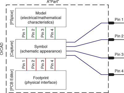 |
| Figure 1-1 The pieces of a “part.” |
The pins on a Capture part can be mapped into the pins of a PSpice model or the pins of a physical package in PCB Editor. PSpice is a CAE tool that contains the mathematical models for performing simulations, and PCB Editor is a CAD tool that converts a symbolic schematic diagram into a physical representation of the design. Netlists are used to interconnect parts within a design and connect each of the parts with its model and footprint. In addition to being a CAD tool, PCB Editor also functions as a front-end CAM tool by generating the data on which other CAM tools operate when manufacturing the printed circuit board (PCB). Combining all three applications into one package produces a powerful set of tools to efficiently design, test, and build electronic circuits. The key to successful project design and production is in understanding the PCB itself and knowing how to use the tools that build the PCB.
Printed Circuit Board Fabrication
We now look at how PCBs are manufactured for a better understanding of what we are trying to accomplish with PCB Editor and why. A PCB consists of two basic parts: a substrate (the board) and printed wires (the copper traces). The substrate provides a structure that physically holds the circuit components and printed wires in place and provides electrical insulation between conductive parts. A common type of substrate is FR4, which is a fiberglass/epoxy laminate. It is similar to older types of fiberglass boards but is flame resistant. Substrates are also made from Teflon, ceramics, and special polymers.
PCB Cores and Layer Stack-Up
During manufacturing the PCB starts out as a copper clad substrate as shown in Figure 1-2.
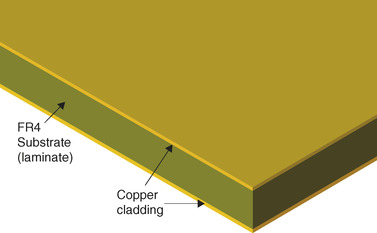 |
| Figure 1-2 A double-sided copper clad FR4 substrate. |
A rigid substrate is a C-stage laminate (fully cured epoxy). The copper cladding may be copper plated onto the substrate or copper foil glued to the substrate. The thickness of the copper is measured in ounces (oz) of copper per square foot, where 1.0
oz/ft
2 of copper is approximately 1.2–1.4 mils (0.0012–0.0014 in.) thick. It is common to drop “/ft
2” and refer to the thickness only in oz. For example, you can order 1
oz copper on a ⅛-in.-thick FR4 substrate.
A substrate can have copper on one or both sides. Multilayer boards are made up of one or more single- or double-sided substrates called
cores. A core is a copper-plated epoxy laminate. The cores are glued together with one or more sheets of a partially cured epoxy, as shown in Figure 1-3.
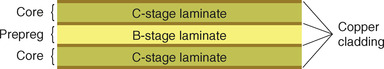 |
| Figure 1-3 Cores and prepreg. |
The sheets are also referred to as
prepreg or
B-stage laminate. Once all of the cores are patterned (described next) and aligned, the entire assembly is fully cured in a heated press.
There are three methods of assembling the cores when making a multilayer board. Figure 1-4 shows the first two methods in an example with four routing layers and two plane layers. Figure 1-4 (left) shows three (double-sided) cores bonded together by two prepreg layers, while Figure 1-4 (right) shows the same six layers made of two cores, which make up the four inner layers, bonded together by one prepreg layer. The outer layers in this panel are copper foil sheets bonded to the assembly with prepreg.
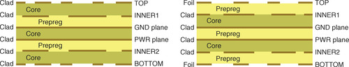 |
| Figure 1-4 Two stack-up methods for a six-layer board: left, multicore, outer clad; right, multicore, outer foil. |
The routing layers in Figure 1-4 are shown as patterned copper segments, and the plane layers are shown as solid lines. The inner layers are patterned prior to bonding the cores together. The outer layers are patterned later in the process, after the cores have been bonded and cured and most of the holes have been drilled. Because the outer layers are etched later and copper foil is typically less expensive than copper cladding, the stack-up shown in Figure 1-4 (right) is more widely used.
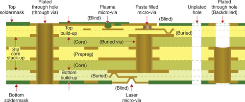
The third method uses several fabrication techniques by which highly complex boards can be fabricated, as illustrated in Figure 1-5. This circuit board may have a typical four-layer core stack-up at its center, but additional layers are built up layer by layer on the top and the bottom, using sequential lamination techniques. The techniques can be used to produce blind and buried vias as well as typical plated through-hole vias, nonplated holes, and back-drilled plated through holes. Resistors and capacitors can also be embedded into the substrate. More about blind vias is discussed in later chapters (Chapter 8 and Chapter 9).
 |
| Figure 1-5 A built-up, multitechnology, PCB stack-up. |
PCB Fabrication Process
The copper traces and pads seen on a PCB are produced by selectively removing the copper cladding and foil. Two methods are commonly used for removing the unwanted copper: wet acid etching and mechanical milling. Acid etching is more common when manufacturing large quantities of boards because many boards can be made simultaneously. One drawback to wet etching is that the chemicals are hazardous and must be replenished occasionally, and the depleted chemicals must be recycled or discarded. Milling is usually used for smaller production runs and prototype boards. During milling, the traces and pads are formed by a rotating bit that grinds the unwanted copper from the substrate. With either method, a digital map is made of the copper patterns. The purpose of CAD software like OrCAD PCB Editor is to generate the digital maps.
Note: Only one layer is considered in the following explanation of the fabrication process.
Photolithography and Chemical Etching
Selectively removing the copper with etching processes requires etching the unwanted copper while protecting the wanted copper from the etchant. This protection is provided by a polymer coating (called
photoresist) deposited onto the surface of the copper cladding, as shown in Figure 1-6.
 |
| Figure 1-6 A copper clad boardcoated with photoresist. |
The photoresist is patterned into the shape of the desired printed circuit through a process called
photolithography. The patterned resist protects selected areas of the copper from the etchant and exposes the copper to be etched.
The two steps to photolithography are patterning the photoresist and developing it. Patterning is accomplished by exposing the resist to light (typically ultraviolet), and developing it is accomplished by washing it in a chemical bath. The two types of photoresist are positive resist and negative resist. When positive resist is exposed to ultraviolet (UV) light, the polymer breaks down and can be removed from the copper. Conversely, negative resist shielded from UV light is removed.
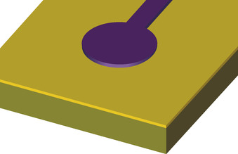
A mask is used to expose the desired part of the photoresist. A mask is a specialized black and white photographic film or glass photoplate on which a picture of the traces and pads is printed with a laser photoplotter. Two types of masks are shown in Figure 1-7.
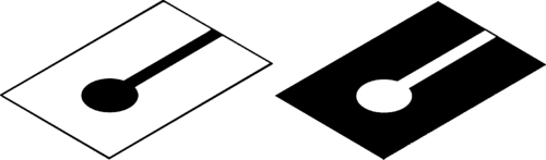 |
| Figure 1-7 Photolithography masks: (left) positive mask, (right) negative mask. |
The masks are examples of a trace connected to a pad. Figure 1-7 (left) shows a positive mask used to expose positive photoresist, and Figure 1-7 (right) shows a negative mask used to expose negative photoresist. Masks that will be used repeatedly are sometimes produced on glass photoplates instead of film.
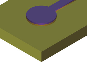
The mask is placed on top of the photoresist, as shown in Figure 1-8 and the assembly is exposed to the UV light. The dark areas block UV light and the white (transparent) areas allow the UV light to hit the photoresist, which imprints the circuit image into the photoresist. A separate mask is used for each layer of a circuit board. OrCAD PCB Editor generates the data that the photoplotter uses to make these masks.
 |
| Figure 1-8 Positive photomask onphotoresist-coated board. |
Another way of exposing the photoresist is by using a programmable laser to “draw” the pattern directly onto the photoresist. This is a newer technique, called
laser direct imaging (LDI). A benefit of the LDI process is that it uses the same data as the photoplotters but no masks are required.
After the photoresist has been exposed (either with the mask and UV or with the laser), it is washed in a chemical called the
developer. In the case of positive resist, the resist breaks down during exposure and is removed by the developer. In the case of negative resist, the UV light cures the resist, and only the unexposed resist is removed by the developer. Common developers are sodium hydroxide (NaOH) for positive resist and sodium carbonate (Na
2CO
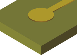
3) for negative resist. Once the resist has been exposed and developed, a circuit image made of the photoresist is left on the copper, as shown in Figure 1-9.
 |
| Figure 1-9 Developed photoresiston copper. |
Next, the board is etched in a corrosive solution, such as alkaline ammonia or cupric chloride. The etching solution does not significantly affect the photoresist but attacks the bare copper and removes it from the substrate, leaving behind the resist-coated copper, as shown in Figure 1-10.
 |
| Figure 1-10 Unwanted copper removed by etching. |
Some processes use a plated tin alloy as the etch resist. The tin alloy plating is more resistant to etchants and preprepares the copper surface for solder processes. In this case, photolithography processes are used to selectively plate the circuit pattern onto the copper surfaces prior to etching.
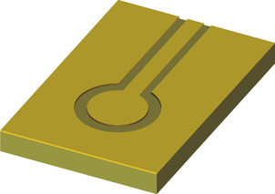
When polymer etch resists are used, the photoresist is cleaned from the copper with a resist stripper, leaving behind the copper traces. Figure 1-11 shows the final patterned copper. When metal etch resists are used, the plating is typically left in place. Holes for the leads and so forth are not etched into the pads because they are drilled after all of the cores have been glued together (later in the process) to ensure proper alignment of the holes between board layers.
 |
| Figure 1-11 Copper pad and trace after etching and resist stripping. |
Mechanical Milling
As mentioned previously, milling is an alternative to etching. To mill the board, a computer numerical control (CNC) machine is programmed with the digital map of the board and grinds away the unwanted copper. The unwanted copper can be completely removed (like that in Figure 1-11), or just enough copper may be removed to isolate the pads and traces from the bulk copper, as shown in Figure 1-12. Removing only enough copper to isolate the traces from the bulk copper reduces milling time but can affect the impedance of the traces.
 |
| Figure 1-12 A mechanically milled trace. |
Layer Registration
After the inner layers have been patterned, the cores are aligned (called
registration) and glued together. Registration is critical because the pads on each layer need to be properly aligned when the holes are drilled. Registration is accomplished using alignment patterns (called
fiducials) and tooling holes in the board, which slide onto guide pins. With the cores in place and properly aligned, a heated press cures the assembly.
After the assembly is cured, holes are drilled for through-hole component leads and vias. The drilling process inevitably heats the laminate due to friction between the laminate and the high-speed drill bit. This tends to soften the laminate and smear it across the walls of the drilled copper. After the drilling processes are finished, the assembly is placed into a bath to etch back the laminate slightly and clean the faces of the copper pad walls. This is called
laminate etchback or
desmear.
Once the holes have been drilled and desmeared, a physical path exists between pads on different layers, but as Figure 1-13 (left) shows, there is no electrical connection between them. To make electrical connections between pads on different layers, the board is placed into a plating bath that coats the insides of the holes with copper, which electrically connects the pads, hence, the term
plated through holes. The plating thickness varies but is typically about 1
mil (0.001 in.) thick. The cutaway view of Figure 1-13 (right) shows a plated through hole on an internal layer of a PCB. The top and bottom copper is actually patterned
after the plating process is finished because the plating process would replate the areas where copper had been removed.
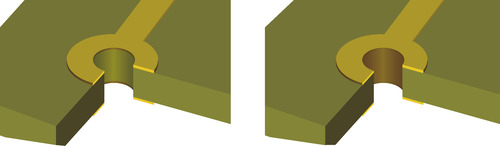 |
| Figure 1-13 Holes are drilled into the board and copper plated: (left) a nonplated through hole, (right) a plated through hole. |
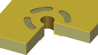
Not all layers have traces. Some layers are planes (see Figure 1-14). Plane layers are typically used to provide low-impedance (resistance and inductance) connections to power and ground and to provide easy access to power and ground at any location on the board. Plane layers and impedance issues are discussed in Chapter 6. The leads of components are connected to ground or power by soldering them into plated through holes. Since copper conducts heat well, soldering to a plane layer could require an excessive amount of heat, which could damage the components or the plating in the hole (called the
barrel). Thermal reliefs are used, as shown in Figure 1-14, to reduce the path for heat conduction but maintain electrical continuity with the plane.
 |
| Figure 1-14 A connection to a plane layer through a thermal relief. |
Since ground and power planes are often inner layers and signal layers will likely be above and below them, in some instances, a via will run through a plane layer but must not touch it. In this case, a “clearance” area (shown in Figure 1-15) is etched into the plane layer around the via to prevent a connection to the plane. The clearance is larger than the normal pad size to ensure that the plane stays isolated from the plated hole.
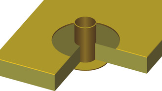 |
| Figure 1-15 A clearance area provides isolation between a plated hole and a plane. |
After the through holes are plated, the top and bottom layers are patterned using the photolithograpy process as described for the inner layers. After the outer copper has been patterned, the exposed traces and plated through holes can be tinned (although tinning is sometimes deferred until later). Nonplated holes (such as for mounting holes) may be drilled at this time.
Next, a thin polymer layer is usually applied to the top and bottom of the board. This layer (shown in dark green in Figure 1-16) is called the
soldermask or
solder resist. Holes are opened into the polymer using photolithography to expose the pads and holes where components will be soldered to the board. The soldermask protects the top and bottom copper from oxidation and helps prevent solder bridges from forming between closely spaced pads. Sometimes openings in the soldermask are not made over small or densely placed vias (called
tenting a via). Tented vias are protected from having chemicals such as flux from becoming trapped inside the hole. Tenting also prevents solder migration into the hole, which could lead to poor solder joints on small components that are close to and connected to the via.
 |
| Figure 1-16 Final layers are the soldermask (dark green) and silk screen (white). |
Finally, markings (called the
silk screen) are placed on the board to identify where components are to be placed. The silk screen is shown in white in Figure 1-16.
Function of OrCAD PCB Editor in the PCB Design Process
PCB Editor is used to design the PCB by generating a digital description of the board layers for photoplotters and CNC machines, which are used to manufacture the boards. Separate layers are used for routing copper traces on the top, bottom, and all inner layers; drill hole sizes and locations; soldermasks; silk screens; solder paste; part placement; and board dimensions. These layers are not all portrayed identically in PCB Editor. Some of the layers are shown from a positive perspective, meaning what you see with the software is what is
placed onto the board, while other layers are shown from a negative perspective, meaning what you see with the software is what is
removed from the board. The layers represented in the positive view are the board outline, routed copper, silk screens, solder paste, and assembly information. The layers represented in the negative view are drill holes and soldermasks. Copper plane layers are handled in a special way, as described next.
Figure 1-17 shows routed layers (top and bottom and an inner, for example) that PCB Editor shows in the positive perspective. The background is black and the traces and pads on each layer are a different color to make it easier to keep track of visually. The drill holes are not shown because, as mentioned already, the drilling process is a distinct step performed at a specific time during the manufacturing process.
 |
| Figure 1-17 Copper in routed layers. |
Figure 1-18 shows examples of drill symbols and silk screen representations used by PCB Editor (traces not shown). The red shapes are examples of drill symbols that indicate locations of the drill holes and are used in conjunction with a drill chart (see Figure 1-19)
, which produces ID numbers for the different drill tools. The white print is the silk screen discussed previously.
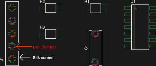 |
| Figure 1-18 Circuit layout with drill symbols and silk screen on a PCB. |
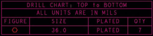 |
| Figure 1-19 Drill chart with drill symbols and specifications. |
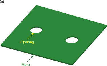
Figure 1-20(a) shows the soldermask with the patterned holes that allow access to pads, and Figure 1-20(b) shows the negative representation used by PCB Editor. Here
, the black background is actually the polymer film and the green circles are the holes in the soldermask.
 |
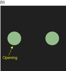 |
| Figure 1-20 Soldermask layer and negative view: (a) soldermask, (b) negative view in PCB Editor. |
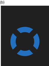
Plane layers are processed as negative layers in PCB Editor and are used to generate negative image Gerber files. However
, PCB Editor displays plane layers in the positive view. Figure 1-21(a) shows a physical copper plane layer with a thermal relief for a pin or via, Figure 1-21(b) shows the negative view, and 1
–21(c) shows the representation displayed by PCB Editor in
“what you see is what you get
” (WYSIWYG) mode.
 |
 |
 |
| Figure 1-21 Copper in a plane layer: (a) copper plane with thermal relief, (b) negative view as processed, (c) displayed in WYSIWYG mode. |
Design Files Created by PCB Editor
PCB Editor Format Files
When you are designing a board, PCB Editor works with and saves the design in a format that is efficient for the computer. The PCB Editor design file has a .brd extension. When you are ready to fabricate the board, PCB Editor processes the design and converts it into a format that the photoplotters and CNC machines can use. These files are called
Gerber files.
Artwork (Gerber) Files
Artwork (Gerber) files are created for each of the etch and mask layers discussed previously, and drill files are created for both plated and nonplated holes. PCB Editor generates as many as 30 or so layer files to describe various manufacturing aspects of the PCB. Some examples of these files, their extensions, and their functions are listed in Table 1-1.
These and other files that PCB Editor generates are discussed in greater detail in the next two chapters and in the PCB Design Examples.
PCB Assembly Layers and Files
Several layer files generated by PCB Editor are not part of the actual fabrication process. These files are used for automated assembly of a finished board and are mentioned only briefly here. The first layer is the solder-paste layer. It is used to make a contact mask for selectively applying solder paste onto the PCB’s pads so that components can be reflow soldered to the board. There may be one solder-paste layer for the top side of the board and one for the bottom side, as indicated in Table 1-1. The second layer file is the assembly layer, which contains information for board assemblers as to the part type, its position, and its orientation on the board. As with the soldermask, there may be one assembly layer for the top side of the board and one for the bottom side. PCB design for the various soldering and assembly processes is discussed in Chapter 5.
The purpose of this chapter has been to introduce you to the process by which PCBs are manufactured. The purpose of the next chapter is to show you how to use OrCAD PCB Editor to design a board and generate the files needed to manufacture the PCB.
..................Content has been hidden....................
You can't read the all page of ebook, please click here login for view all page.