1
Electric and Magnetic Fields
Buildings have walls and halls.
People travel in the halls, not the walls.
Circuits have traces and spaces.
Energy travels in the spaces, not the traces.
Ralph Morrison
1.1 Introduction
I have written many books that discuss electricity. The sixth edition to my Grounding and Shielding was published in 2016. Each time I start to write, it is because I have added to my understanding and I feel I can help others solve practical problems. The digital age is upon us and it is making demands on design that are not covered by circuit theory. In one sense, logic is easier to handle than sine waves as there is no phase shift to consider. As clock rates rise there are a host of other problems that must be considered. The tools of circuit theory are in many ways a mismatch for fast circuits and some new methods need to be introduced. Circuit theory does not consider time of transit and this is a key issue in logic design.
The insight that has led me to write this book involves one key word and that word is energy. Engineers are taught that stored energy can do work and that there is conservation of energy. What I want to point out is that all electrical phenomena is the movement or conversion of energy. When a logic signal is placed on a trace, the voltage that is present means that energy was placed on a capacitance. This energy had to be moved into position and it had to be done in a hurry. It cannot be done in zero time as this would take infinite power. The movement of voltage in circuit theory does not mention moving energy and that one fact leads to many difficulties. For example, energy is not carried or stored in conductors. It is carried and stored in spaces. This requires a different point of view. Providing this insight is the reason for writing this book.
I am writing this book to help you avoid problems when laying out digital circuit boards. This first chapter is about the fundamentals of electricity. You may opt to skim over this material but I would hope to change your mind. I want to show you how electricity works but not from a circuit theory viewpoint. I want to show you how to use the spaces that carry energy between components. This may be a new way for you to view electricity. Circuit theory pays little attention to spaces. Conductors outline the spaces used by nature to move field energy.
I am writing this book to describe the role fields play in moving energy on transmission lines. Most of the literature relating to transmission lines revolves around sine waves. There are insights to be gained when step functions are applied to moving energy. These insights can help you in today’s designs and prepare you for the future which is headed in the direction to move more and more digital data. Whatever the future holds, fundamentals apply.
This opening chapter will help to set the stage for discussing transmission lines. Once you see how nature really works, you will find it easy to accept the material in the later chapters. I have spent my career learning and applying this material and I know why basics come first. What is even more important is connecting these basics to real issues and that is not always easy. That is my objective in writing this book.
It is worth a moment to describe a problem in understanding. In reading posted online material, the language that is used often implies a picture of electrical behavior that is invalid. A writer may say that “—the return path impedance is too high.” The impedance of a transmission path is really the ratio of electric and magnetic fields involving the space between the forward and return current conductors. It is incorrect to treat the forward and return paths this way. It takes care in the use of language and a clear understanding of basics to communicate clearly. In this book I have chosen my words carefully and I hope they are read with the same care. I realize there are strange explanations that must be unlearned and that is not always easy to do. Currents do not travel one way on the surface of a conductor and return down the middle of that same conductor. I will not spend time trying to argue this point.
There are many ways to learn electronics. Diagrams that include connections between components are common. These diagrams make no attempt to suggest that energy is flowing in the spaces between the connections. It is through experience that an engineer learns that component locations and wiring methods are important. Understanding the mechanisms involved is presented in this book. What is hard to accept is that there are a lot of habit patterns that develop over the years. Some of these patterns may work at the time but lead to problems as the logic speeds increase. Looking back, I can say that many published application notes I tried to apply were invalid.
A good example of the problem exists in the wiring to a metal case power transistor. A metal case provides for heat transfer as well as a connection to the die. The fields that move electrical energy cannot enter or leave through the metal case. Fields can only use the space around the connecting pins. This results in fields sharing the same space which is feedback. I remember discussions on how to mount these devices that involved surface roughness but never a discussion of field control. Because the circuits worked, I did not question the printed page.
If surface roughness was a consideration, it also meant that the characteristic impedance of the energy path was important and this was not mentioned. This issue will become clearer in later chapters.
We live in an electrical world. Atoms are made of electrical particles. All the energy that comes from the sun is electrical. As humans, our brains and nerves are electrical. We have used our understanding of electricity to communicate, travel, and entertain ourselves. We have learned to use electricity to light our cities and to run our industries. Today’s electronics gives us computing power that invades every aspect of life.
Most of the energy we get from the sun each day is electrical. We also get energy from the hot core of the earth and some of it comes from the gravitational field of the earth/moon. The sun has stored energy for us in the form of coal and petroleum. On a daily basis, the sun’s energy grows our food, heats our land, evaporates ocean water, and moves our atmosphere allowing us to live our lives. The actions of nature are in effect unidirectional. Sunlight is converted to heat but not the other way around. Water runs downhill except where trapped in pools. Air runs out of a balloon. We know how to put air back into the balloon, but it requires some other device that releases stored energy.
The game of life is the motion of energy through a vast complex of matter. One of our engineering goals is to perform logic functions. We can accomplish this task by providing pathways for nature to move energy. This energy flow is in the form of electric and magnetic fields. We use these fields because they are fast, efficient, inexpensive, repeatable, and available. The problem we face is how to do this with the materials we have at hand. To be effective, we need to know the rules nature will follow as we select and configure materials to build our circuits. Nature is very consistent.
A good place to start is to move some energy. A dropped stone gives motion to air as it gains kinetic energy. On impact, some of the energy is converted to sound, mechanical vibration, and heat. The total energy is conserved but it is no longer energy of position in a field of gravity. The energy cannot return to its initial state. In the case of a pendulum, potential and kinetic energy can move back and forth, but there is always friction that will remove energy and in time the pendulum will stop moving. I like to call this nature running down hill. The basic explanation involves a concept known as entropy. All systems tend to “spread out” if given an opportunity. We rely on nature to take this action. When we connect a resistor to a battery we expect it to get hot. If we poke a hole in a pail of water, we expect water to drain out. If we connect a voltage to a pair of conductors, we expect energy will flow between the conductors. Nature does this the same way over and over, never changing the rules. The way energy moves on a circuit board is the subject of this book. I want to show you nature’s rules so we can perform needed tasks. It sounds trite to say this but it is important. We can follow nature’s rules but she will not follow ours. I do not care who signs the documents.
Circuit theory is key in the education of electrical engineers. The physics of electricity is taught but the connection to practical issues is not always a goal. This is not surprising as there are so many possible specialties and applications. The basics are taught and it is assumed the engineer will make the needed connections on his own. Electrical engineers are taught circuit theory that handles linear and active circuits using sine waves up to frequencies of several MHz. The basic assumption made by circuit theory is that an analysis based on how ideal circuit elements are interconnected tells the full story. This viewpoint sidesteps the issue of field theory and energy transfer which are needed to move logic. At frequencies above a few MHz, circuit theory begins to show its inadequacies. To add to the problem, logic signals are not sine waves which are the basis of circuit theory. Take away circuit theory and stay away from field theory and it becomes a big guessing game. Engineering and guessing are not compatible. Engineers that start their design activities using circuit theory rarely try to use field theory to solve problems. A change in approach will only occur if someone understands the need for change.
The fundamentals of electricity are properly expressed in terms of partial differential equations. These equations are difficult to use even with computer assistance. The solutions that are provided revolve around sine waves and logic has voltage signals that are step and square waves. Even if the engineer is a skilled mathematician it is not practical to find exact solutions using field equations. The mathematics tells a story that is very compact. Very few can understand the full story by just reading equations. Until recently, a common‐sense approach to interconnecting components on a circuit board was quite satisfactory. This approach has limitations specifically at high bit rates. When there are problems, the only approach is to go back to basics. It turns out a lot of insight can be gained by applying the basic principles of physics. The simplifications offered by circuit theory have reached a limit. What is not appreciated is that circuit theory lets us make many false assumptions that become habit patterns. The difficult part of applying physics to fast logic is not the new ideas, but the letting go of assumptions that have been made and that we are not aware of. The most troublesome assumption is that conductors carry energy. Conductors direct fields and fields carry energy in spaces. I will say this over and over again. This is the inverse of what most people sense.
When I started to design circuits, I soon learned there were issues that had to be faced at every corner of my reactance chart. Small parasitic capacitances were everywhere. Resistors above 100 megohms were not resistors above 100 kHz. Magnetic materials were extremely nonlinear. I found out that capacitors had natural frequencies and that any feedback circuit I built was guaranteed to oscillate. I found out that power transformers coupled me to the power lines and test equipment connected my circuits to earth. Every time I started working on a new product the real world presented me with a new set of problems. Most of these problems were not discussed in any textbook. These were problems that were not helped by using mathematics. Laying out digital circuit boards is no different. There is a lot to learn before designs are free of problems. This is particularly true as clock rates enter the GHz range. Understanding compromise requires understanding fundamentals. Good engineering requires a lot of compromise. The problem is compromise must be based on understanding.
Logic circuits are mainly the interconnection between various integrated circuits. It takes experience to realize that these interconnections must be designed. Connecting logic components together is the subject of this book. Until problems start to appear, the designer is not apt to think of applying any change in approach. In analog design, I found out that microvolts of coupling occurred if I was not careful in interconnecting components. Usually this meant avoiding placing any open spaces in the signal path. A similar set of problems occurs in logic. The voltage levels that cause errors are greater but so is the frequency content. In both cases, it is the same basic electrical phenomena that must be understood. In very simple terms, keep all transmission fields under tight control.
In the digital world, it is not practical to experiment with layout. A redesign is expensive and it takes time. Tests to prove conformance with regulations are expensive. Making measurements that can isolate problems also has its difficulty. A practical sensor can pick up signals from a dozen sources. An identification of which source is causing a problem is not usually possible. Wiring on the inner layers of a circuit board is not accessible. Parts of the transmission are inside an IC package and there is no way to view these signals. The list of difficulties is long. All factors need to be considered at the time the traces are located. These factors are the subject of this book.
In the following chapters, I discuss logic transmission in terms of step functions. There is no simple mathematics that fits this type of signal. Circuit theory and sine waves were made for each other but logic requires different tools. It is not all that complicated but it is different. It takes time to study, review, and accept a new set of ideas and routines and put them to practice. What may not be appreciated is that there is insight that can be gained by using step functions that is hidden when sine waves are used. I point out these insights as I write.
We use some mathematics to discuss the principles of field theory. This will help in explaining what is happening on a logic circuit board as the clock rates cross into the GHz region. An understanding of differential equations and vector analysis is not a requirement for understanding the material in this book. I use both language and mathematics to explain each topic. For some, the language of physics will be new. Both circuit components and the way they are interconnected will be important. An understanding will eventually lead the designer to follow good practices. Taking this view will make it possible to design circuit boards without making false assumptions. Once the rules are known, they become the new habit pattern. The designer must keep the basics in mind.
I assume the reader is familiar with the language and the diagrams of circuit theory. I want to caution the reader that diagrams often suggest meaning that is misleading. A good example is the symbol for an inductor. A coil of wire has inductance but so does a straight conductor. A trace over a ground plane also has inductance as well as a volume of space. Extending the understanding of inductance is an objective in this book.
The symbol for a capacitor is another example. The symbol with its symmetrical connections gives the impression that current arrives at the center and spreads out symmetrically. What really happens is that current enters at one end and is associated with a magnetic field. As you will see, a capacitor looks more like transmission line than a component. This is a picture not suggested by the symbol.
Another example of how we are misled is the diagram for a transformer. The last turns of a primary coil are capacitively coupled to the first turns of a secondary coil. The diagram implies some sort of symmetry which is rarely present. I am not suggesting a different symbol only an awareness that we tend to make assumptions. When we read we do not check spelling but a misspelled word sticks out. This same understanding can take place in board layout. Schematics and wiring lists tend to hide issues of layout. It may become necessary to add a requirement that a signal flow chart be a part of each design. It is an important part of a design.
Logic has become so complex and proprietary that the structure inside a component is rarely made available. The compromises taken by the manufacturer are not discussed with the user. The user assumes that the logic will function at the specified clock rates. The manufacturer decides just how much information the user needs to know.
The language of electricity is not always clear. There are words we use with literally hundreds of meanings. Two examples are the words ground and shield. Some words can represent a vector or a scalar and without help, the reader is left guessing. Both the writer and the reader have a responsibility to be careful in treating the written word. Often the meaning depends on context. Read with an open mind. Hopefully the picture will grow in clarity as more and more examples of the issues are presented. The glossary at the end of each chapter is there as a reminder of how much attention we must pay to language.
In any rapidly changing field there is a tendency to invent language, whether needed or not. Acronyms often become new words. In this book, an effort will be made to use well‐established language including terms used in physics. Words change their meaning through usage and sometimes the meaning is transitory. I want to use language that makes sense to old‐timers as well as to the next generation of engineers. I expect that newcomers will need all the help they can get. I will avoid acronyms as they are not always stable. I have attended meetings where disagreements have occurred because two definitions of one acronym were involved.
This book does not discuss logic diagrams, the choice of components, software methods, or clock rates. Our interest is in describing how to move energy so that the functions taking place are performed without introducing errors or causing radiation.
1.2 Electrons and the Force Field
An electron is a basic unit of negative charge. It has the smallest mass of any atomic particle. In an atom, electrons occupy quantum states around a nucleus. Chemistry is a subject that treats the formation of stable molecules when elements share electron space. The simplest atom is hydrogen which has one electron and one proton. All other elements have both protons and neutrons in a nucleus and electrons in positions around this core. A proton has a positive charge that exactly balances the negative charge of an electron. When an electron leaves an atom, the empty space behaves as a positive charge. In effect the field of a proton has no place to terminate inside the atom. Another way to treat positive charge motion is to compare it to the motion of an empty seat in an auditorium. If a person moves left into an empty seat the space moves right. In a semiconductor, the absence of an electron is a hole that has a different mobility than an electron. In a conductor, the mobility of a vacant space is the same as an electron. In electronics, we consider that all protons are captive and will not leave an atom to partake in current flow. We also assume that the atoms in a conductor do not move any distance.
Copper atoms have 29 electrons with 1 outer electron that is free to move between atoms. Avogadro’s number tells us that in 63.54 g of copper there are 6.02 × 10²³ atoms. This is the number of electrons in this amount of copper that can move freely between atoms. I am giving you these numbers so that you can better appreciate what really happens in a typical circuit. I think you are going to be very surprised by the story I am going to tell you.
We know there are forces between electrons. When hair is combed on a dry day, the individual strands of hair will separate and stand straight out. In a clothes drier, the rubbing action can move electrons between items of clothing that can create a glow seen in a dark room. We have all seen the power of lightning1 where rain strips electrons off of air molecules and carries charge to earth. In the laboratory on a dry day, it is possible to rub a silk cloth on a glass rod and transfer electrons from the rod to the silk. The rod is said to be charged positive. Touching this rod to hanging pith balls will cause the balls to swing apart. If the cloth rubs a hard rubber rod, then electrons are added to the rod. When the hard rubber rod touches one of the pith balls, the two balls will attract each other. If the pith balls are metalized, then the charges will move on the conducting surface until there is a balance of electrical and mechanical forces. In this case, the electrons cannot leap out into space and the forces appear to be between the pith balls. These forces are actually between charges. These forces are shown in Figure 1.1.

Figure 1.1 The forces between charges. (a) Repelling force and (b) attracting force.
When there are forces at a distance it is usual to call the force pattern in space a field. In the example above, the force field is called an electric or E field. Fields have both intensity and direction at every point in space. The field we are most familiar with is gravity. On earth the gravitational field pulls each of us toward the center of the earth with a force equal to our mass. 4000 miles out in space, the force would be reduced by a factor of 4. The electric field behaves the same way. A negative charge located on a conducting sphere of radius R creates a force field. A small positive test charge near the sphere will be attracted with a force F. If the test charge is moved out to a distance 2R, the force will be reduced by a factor of 4. We will have a lot to say about electric fields. Later we discuss the magnetic field, which is a force field of equal importance. This field is quite different because the motion of charges creates forces at a distance.
Here is another observation that is worth discussing. The chemical properties of elements depend on the number of electrons available to interact with other elements. In our circuits, there is no evidence that the properties of materials change when large currents flow. We do see property changes when materials are dissolved in a solution. That is because all of the atoms are involved, not a very small percentage.
Now you know that the percentage of electrons involved in circuit activity is very near zero. It is easy to show that the velocity of electrons in a typical circuit is under centimeters per second. This is technically known as electron drift. We know that signals on a circuit board travel at the speed of light. This says that we should focus on the field that surrounds the electron, not on the electron itself. This is because electrons are a slow mover in every sense. The problem is they keep bumping into atoms. The force field is potent as we have discussed.
The changing of an electric field creates a magnetic field. This fact is stated in Maxwell’s field equations. The fact that the electric and magnetic field act together to move energy is at the center of all electrical activity. We discuss the magnetic field after we have discussed the electric field. Then we discuss how the two fields act together to move energy along transmission lines. Of course fields also move energy in free space but not at dc.
On earth, we live in a force field called gravity. The force field around a mass is proportional to that mass and falls of as the square of distance. In gravity, the fields between masses always attract; they never repel. A gravitational field is called a weak field. After all it takes the mass of the entire earth to attract a 150‐pound person with a force of 150 pounds. There are several other force fields in nature and they exist in the nucleus of the atom. These fields are a topic for a course in nuclear physics.
1.3 The Electric Field and Voltage
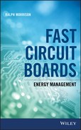
Before we can talk about moving logic signals, we need to discuss electric and magnetic fields and the definition of voltage. We start our discussion by placing a group of electrons on a small mass. We call this a unit test charge Δq. We then deposit a larger charge Q on a conducting sphere. These charges spread out evenly on the surface of this sphere creating an electric field around the sphere. When the test charge is brought into this field created by Q, the force between the two fields is sensed on the two masses. The repelling force is
where r is the distance to the center of the sphere and ε0 is a constant called the permittivity of free space. It is a fundamental constant in nature. This equation states that the force between two charges falls off as the square of the distance between the charges. The constant ε0 is equal to 8.85 × 10⁻¹² farads per meter (F/m). We discuss the farad when we discuss capacitance.
A test charge must be small enough so that the charge distribution on the sphere is not disturbed by its presence. The force per unit charge in the space around the sphere is called an electric or E field. This E field intensity at a radial distance r from the center of the sphere is given by the equation

The E field is called a vector field because it has intensity and direction at every point in space. This force field is proportional to charge and inversely proportional to the square of distance from the center of the sphere. The force direction on the test charge is in the radial direction.
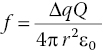
Work is simply force times distance, where the direction of the force and the travel direction are the same. If the force is at an angle to the direction of motion, the work equals force times distance times the cosine of the included angle. The work required to move a unit charge from infinity to the surface of a charged sphere is given by Equation 1.3. The simplest path of integration is along a radial line that starts at infinity and goes to the surface of the sphere. Actually, if you do the mathematics correctly, any path will give the same answer. Using Equation 1.1, the voltage V on the spherical surface is
This equation tells us the amount of work required to move a unit of charge from a large distance to the surface of the charged sphere.
Comparing Equation 1.3 with Equation 1.2, it is easy to see that the intensity of the electric field E at the surface of the sphere is V/R and that E has units of volts‐per‐meter.
Equation 1.3 can be used to determine the voltage between conductors as well as between points in space. This is shown in Figure 1.2 where the conducting sphere is at a potential of 5 V. If the integration were to stop at 4 V, it would be on an imaginary spherical surface that surrounds the conducting sphere. This sphere is called an equipotential surface. It takes no work to move a test charge on an equipotential surface in space or on the surface of a conductor.

Figure 1.2 Equipotential surfaces around a charged sphere.
The radial lines represent the force field direction. These lines terminate perpendicular to the conducting surface. If there were a component of the E field parallel to the conducting surface it would imply current flow on the surface. There can be no E field inside of the conducting sphere as this would again imply current flow. At room temperatures, electrons cannot leave the surface of the sphere. Extra electrons space themselves uniformly on the surface to store the least possible amount of energy. This energy is discussed in Section 1.5.
The number of E field lines that we use to describe a field is arbitrary. The intent is to show the shape and relative intensity of the field. One line is assigned to a convenient amount of charge. In a given field pattern, the closer the lines are together, the more intense the field and the greater the force on a unit test charge. In the following diagrams, by convention, lines of force initiate on a positive charge Q and terminate on a negative charge −Q. A positive charge is the absence of negative charge. In Figure 1.2 a charge −Q must exist at infinity. In most of the conductor geometries we consider, the E field lines terminate on local conductors. Since these lines represent field shape, their termination at infinity has only symbolic meaning.
1.4 Electric Field Patterns and Charge Distributions
It is convenient to reference voltages to one conductor in a circuit. The reference conductor is assigned the value 0 V. This reference conductor is also referred to as ground or common. There are voltages between conductors which mean there are fields in the intervening spaces. In an analog system, it is possible to have many reference conductors on one board. A reference conductor can be smaller than a nail head or larger than a computer floor.
Reference conductors are often called ground even though they are not earthed. Electrically the ocean could be called a zero of potential but it is not often called ground. A ship’s metal hull can be called an electrical ground without creating any confusion.
Figure 1.3 shows the electric field pattern for several conductor configurations that include a large conducting ground plane at the zero of potential. No significant work is required to move charges along this surface or along any connected conductors. Assuming no current flow, the voltage on this ground is constant, independent of the charge distribution on its surface. There is a minor conflict here because there are tangential forces needed to space these charges uniformly apart on the surface. These fields are small and not the subject of this book.
Figure 1.3 (a)–(c) Electric field configurations around a shielded conductor.
This is not a treatise on free electrons in conductors. The physics of electron motion in conductors involves temperature. There is an average motion of atoms and electrons that is statistical in nature. This average motion in the presence of a field determines the resistivity that varies with each material. For copper, the resistance increases with temperature. For some alloys the temperature coefficient of resistivity is near zero. Predicting the resistance of conductors from basic principles has not been done. Superconductivity occurs at temperatures near absolute zero. The explanation of this phenomena involves quantum mechanics.
In the field configurations we deal with, the electric field is assumed perpendicular to a conductor’s surface even if there is current flow. To illustrate this point, consider the following example. The spacing between a trace and a ground plane is 5 mils or 1.27 × 10⁻⁴ m. A trace voltage of 5 V means the E field intensity in the space is about 40,000 V/m. The E field in a trace that supports current flow is usually less than 1 V/m. This ratio tells us that the E field has a very small component that is directed parallel to a trace run. For all practical purposes, the lines representing an E field terminate perpendicular to a conducting surface even if there is current flow.
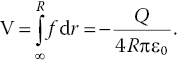
In Figure 1.3a, a small charged sphere A at potential V1 is surrounded by a grounded sphere S. No field lines extend outside of this enclosed space. The field lines from A terminate on the inside surface of S. This means a charge −Q has been supplied to this inner surface. The sphere B has no charges on its surface and it is at zero potential. If voltage V1 changes then charges must be moved from the inside of conductor S to the surface at A. Conductor S is called a Faraday shield. This figure shows that if there is a voltage between conductors, there must be surface charges. There is no exception to this rule. This figure also illustrates a basic shielding principle which is the containment of the electric field.
Figure 1.3b illustrates what happens when a hole is placed in surface S. Some of the field lines from A terminate on conductor B. The result is that a charge Q1 must be located on surface B. This charge was supplied as current on the wire connecting B to ground. If V1 changes, then current must flow in the connecting wire to supply a different Q1. This current is said to be induced. A current flows only when the voltages are changing. If the voltage changes in a sinusoidal manner the current is also a sinusoid.
This figure illustrates several points. If hardware must be shielded, then one hole can violate that shield. A hole is a two‐way street. Not only can a field leave the enclosure, an external field can enter through this hole. What is even more important, one lead entering the enclosure can transport interference in either direction. Remember: It only takes one hole to sink a boat.
Figure 1.3c illustrates what happens when conductor B is floating. There is no way that new charges can be supplied to this surface, so the sum of the surface charges must be zero. The charges on the surface distribute themselves so that charges +Q2 and −Q2 group on opposite sides of the B surface. If V1 changes then obviously currents must flow on the surface of B. These are called induced currents. Notice that there is an accumulation of charge on the ground plane under the floating conductor. There are no measureable potential differences along the ground plane. For a system of ideal conductors with changing voltages, surface currents will flow whenever there are terminating field lines in transition. Do not forget that the percentage of charges in motion is one part in a trillion and yet trillions of electrons are in motion. It is fairly obvious that these electrons are truly on the conducting surface. If there were field lines in the conductor there would be current flow.
Figure 1.4 shows the electric field pattern for a circuit trace at voltage V over a conducting plane at 0 V. The field pattern contains a lot of information. The E field intensity is greatest under the trace. Note that the field lines tend to concentrate at sharp edges and that some of the field lines terminate on the top of the trace. The current flow on the surface of a trace will be greatest where the most field lines terminate. This means that the apparent resistance of a conductor depends on how much of the conductor is used for current flow. Areas where the fields do not terminate have no current flow and cannot contribute to conduction. In many applications where high current is involved the conductor geometry must provide mechanical stability. This does not necessarily imply that current will use all of the conductor.
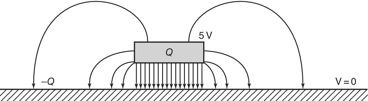
Figure 1.4 The electric field pattern of a circuit trace over a ground plane.
1.5 Field Energy
The work required to move a charge Q up to the surface of a conducting sphere is stored in the electric field around the sphere. There is no other explanation. The temperature is unchanged, there is no mechanical distortion, and there is certainly no chemical change. The same thing happens in the gravitational field. When a pail of water is lifted to a water tank, the gravitational field stores the energy. This concept of space storing field energy is troubling because it defies our senses. We see this movement of gravitational energy in the earth/moon system by observing tidal action. Field energy must also move when a transmission line carries a logic signal. What is actually moving is enigmatic. We discuss energy motion when we discuss transmission lines.
The field in Figure 1.2 extends radially and we know the field intensity at the surface of the sphere. If we consider a plane surface of equal area as in Figure 1.4, we can equate the charge density at the surface with an E‐field intensity. Since the E field is a constant over the area A, the increment of work dW to move a unit charge dq in this field is Eh dq where E equals Q/ε0A,
The work to move a total charge Q is
Since E = Q/ε0A then Q = ε0AE. Using this value of Q in Equation 1.5 the work W is
where V is the volume of the E field space and W has units of joules. The energy E stored in the volume V is equal to this work or
There is field energy stored in the spaces defined by any conductor geometry where there are potential differences. It is important to point out that it is impossible to have a static electric field unless there are materials present. When there are insulators (dielectrics) there can be trapped electrons. We will not consider this phenomenon. In Section 1.6, we show that the presence of dielectrics between conductors will change the field patterns and the amount of energy that is stored.
1.6 Dielectrics
Dielectrics are insulators. Glass epoxy is an insulator used in the manufacture of circuit boards. Other dielectric materials are rubber, mylar, nylon, air, polycarbonates, and ceramics. In Figure 1.3, the space between the trace and the conductor is air. If glass epoxy is inserted between the conductors the electric field will reduce in intensity by a factor of about 4. This reduction factor is called the relative dielectric constant εR. This factor is simply a number with no units. The voltage between the two conductors will drop to V/εR. The E field in Figure 1.4 can now be written as

Insulators and dielectrics play a big role in electronics. Conductors must carry currents between components but they must be supported on insulators, so dimensions are maintained and there is little chance of a voltage breakdown. The characteristics of copper are constant but the insulators that surround copper have continued to evolve. Every insulator is selected for its electrical and mechanical character. Early insulators were paper, Bakelite™, and cloth that have been replaced by glass epoxies, nylon, ceramics, and rubber.
By weight, a circuit board is mostly insulation. As we see in detail, the fields that carry energy use dielectrics and air. The manufacture of circuit boards uses dielectric materials that have proved to be effective. Board designers rely on board manufacturers to select the materials that are best for a design. It is important that board designers stay current with the changing technology. Just another reminder. Energy flows in insulators, not in conductors. The conductors direct where the energy flows. The only energy in the conductors involves moving electrons and this is a tiny fraction of the energy in the space between conductors.
Table 1.1 below lists the relative dielectric constants of some of the common dielectrics and insulators used in electronics.
Table 1.1 The relative dielectric constant for materials used in electronics.
| Material | Relative dielectric constant εR |
| Air | 1.0 |
| Barium titanate | 100–1,250 |
| BST (barium strontium titanate) | 1,000–12,000 |
| Ceramic | 5–7 |
| Glass | 3.8–14.5 |
| Glass epoxy | 3.6–4 |
| Mica | 4–9 |
| Mylar—polyethylene terephthalate (PET) | 5–7 |
| Neoprene | 6–9 |
| Nylon | 3.4–22.4 |
| Paper | 1.5–3 |
| Teflon | 2.1 |
| Water (distilled) | 78 |
It is important to note that water has a high dielectric constant. If moisture is absorbed by a dielectric the dielectric constant will change. This means that circuit boards must be coated with a sealant to keep out moisture. There are several sealants available on the market and the choice is related to production quantities and the need to avoid pins, pads, test points, and connections.
1.7 Capacitance
The ability of a conductor geometry to store charge is called capacitance. It is measured as the ratio of charge stored to applied voltage or
The unit of capacitance is the farad. A farad stores 1 coulomb of charge for a potential of 1 V. The units in common use are usually below a millionth of a farad. Capacitances as small as 10−12 F can be important. This level of capacitance is called a picofarad and is abbreviated as pF. 10−9 F is called a nanofarad, abbreviated as nF. 10−6 F is called a microfarad, abbreviated as μF.
For the sphere using Equation 1.3, the ratio of charge to voltage is
Using Equation 1.10, the capacitance of the earth is 711 μF.
For parallel conducting planes the capacitance is
where A is the surface area and h is the spacing between conductors. This equation can be used to calculate the capacitance of most commercial capacitors. It can also be used for determining the capacitance between conducting planes or the capacitance of a trace over a conducting plane. Assume that a 10‐mil wide, 10‐cm long trace is 5 mils above a ground plane. If the relative dielectric constant is 4 the capacitance is 7.1 pF.
1.8 Capacitors
A capacitor is a conductor geometry that stores electric field energy. There are many types of commercial capacitors that fill a wide range of needs. They can act as filters in power supplies. They can function to block dc in analog circuits. They can act as elements in active and passive filters, function generators, and oscillators. They come in many shapes and sizes and can handle a wide range of voltages. They can weigh a ton or be as small as a pin head. Depending on application they are constructed using many different dielectrics. Most of the capacitors we deal with in this book are called decoupling capacitors. They supply energy to transmission lines and semiconductor components. These capacitors are surface mounted which means they have no leads. The character of these capacitors will be examined in more detail later in this book.
The energy stored in a capacitor is given by Equation 1.12 where V is the voltage, A is the area, and h is the conductor spacing. The energy is thus

Substituting Equation 1.11 into Equation 1.12, the energy equals
The capacitors used on a logic circuit board typically use ceramic dielectrics. The dielectric is often BST (Barium Strontium Titanate). This dielectric material can be formulated to have a dielectric constant as high as 12,000. This high dielectric constant allows the capacitors to be both small and inexpensive. Most circuit boards use dozens of these capacitors. The dielectric constant varies with temperature and voltage. Since the exact capacitance is not critical, this type of capacitor is ideal for supplying energy to transmission lines on a circuit board. The function of these capacitors is discussed in Chapters 2 and 3.
1.9 The D or Displacement Field
It is necessary to have two measures of the electric field. The E or electric field is known when voltages are known. A second measure of the electric field is the D field. Lines of D field start and stop on charges. The D field does not change value across a charge‐free dielectric boundary. The D field allows us to extend the concept of current flow to space. The D field is known when the charge distribution is known. In our discussions, there will be no free charges in space or at dielectric boundaries. There will only be a very small percentage of available charges moving on the surface of conductors.
The D field is known as the displacement field and it is related to the E field by the permittivity of free space and the relative dielectric constant
In Figure 1.5, the D field is continuous between the two conductors. It does not change at the dielectric boundary. The voltage across the two dielectrics must sum to 10 V. The E field in the dielectric is 1/8 the E field in air. The voltage across the dielectric is (E/8) × 5 cm and across the air space is (E/1) × 5 cm. The sum is 10 V. The E field in free space is 1.78 V/cm and 0.233 V/cm in the dielectric. Note that most of the field energy is stored in the air space.2

Figure 1.5 The electric field pattern in the presence of a dielectric.
1.10 Mutual and Self Capacitance
A mutual capacitance is often referred to as a leakage or a parasitic capacitance. On a circuit board where traces run parallel to a conducting plane, some of the field lines will terminate on nearby traces rather than on the plane. This situation is shown on Figure 1.6.

Figure 1.6 The mutual capacitances between traces over a ground plane.
The self‐capacitance of a conductor is the ratio of charge to voltage on a conductor when all other conductors are at zero potential. The ratio of charge on conductor 2 to voltage on conductor 1 with all other conductors grounded is called a mutual capacitance C12. If the charge on conductor 1 is positive, the charge on conductor 2 is negative. Therefore, all mutual capacitances are negative. It can be shown that C12 is equal to C21.
On most circuit boards with short trace runs, mutual capacitances can be ignored. For long trace runs, the cross‐coupling that results can impact signal integrity. This subject is discussed in Section 4.5.
1.11 Current Flow in a Capacitance
In circuit theory, the signals of interest are sine waves. In logic, the ideal signals of interest are step functions of current or voltage. If a steady current I flows into a capacitance C the voltage will increase linearly. The charge that flows is the current in amperes times time or
From Equation 1.9, Q = CV. This means that
The voltage across a capacitor, when supplied a steady current, is shown in Figure 1.7.
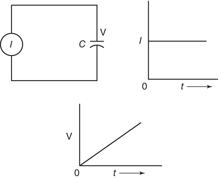
Figure 1.7 The voltage on a capacitor when supplied a steady current.
Mathematically, the current I that flows into a capacitor when the voltage changes with time is
A steady current flowing into a capacitor causes the voltage to rise linearly. The current flow accumulates a charge on the capacitor plates at a steady rate. In circuit theory, a surface charge is not considered and the current flow is assumed continuous through the capacitor. In field theory, a changing displacement or D field is equated to current flow. The changing D field means there are changing charges present on the plates of the capacitor. This concept will be important in the study of waves on transmission lines.
1.12 The Magnetic Field
Magnetic fields and electric fields play an equal role in moving energy. Before we can discuss moving energy, we need to spend some time understanding magnetic fields. When we observe logic signals we look at voltages. The presence of voltage immediately implies an electric field. What may not be appreciated is that moving a voltage between two points requires moving energy and this requires both a magnetic and an electric field. When energy is not moving, the magnetic field is usually zero.
An understanding of magnetic fields is required in the design of transformers, speakers, inductors, motors, generators, MRI hardware, and particle accelerators. Magnetic fields are also required in moving logic signals on traces. Magnetic fields are a part of all electrical activity including electromagnetic radiation. Electromagnetic field energy in motion is always divided equally between electric and magnetic fields. Half the field energy in sunlight is magnetic.
We have all played with permanent magnets and sensed forces at a distance. We can duplicate these same forces when current flows in a coil of wire. A very simple experiment can show the shape of a magnetic field. A wire is passed through a piece of paper holding iron filings. When a steady current flows in the wire, the filings will line up forming circles around the wire. These closed circles show the shape of the magnetic field. The filings line up to minimize the amount of energy stored in the magnetic field.
The atomic structure of some elements allows their internal fields to align. In these materials, we can observe magnetic behavior. Common magnetic materials include iron, cobalt, and nickel. The rare earths samarium, dysprosium, and neodymium are also magnetic. These elements, when properly blended and annealed, provide permanent magnets with very strong magnetic fields. Uses include speakers in our phones and computers. They make electric motors in battery‐powered automobiles practical.
The iron in the earth’s core is magnetized and forms a huge magnetic field that surrounds the earth. A compass needle will align with this magnetic field to indicate direction on the surface of the earth. The earth’s magnetic field concentrates near the earth’s magnetic poles. The Aurora Borealis in the northern hemisphere is caused when electrons that arrive from the sun spiral in the earth’s magnetic field and concentrate near the earth’s north magnetic pole. These electrons ionize air molecules in the upper atmosphere causing radiation in the visible part of the spectrum. In the southern hemisphere the effect is called Aurora Australis.
When current flows in a conductor, there is a magnetic field. When a second conductor carrying current is brought close, there is a force between the two conductors. If the current flows in the same direction, the conductors will attract each other. The attraction and repulsion of magnetic fields is at the heart of motors and generators. This same magnetic field is involved in moving a logic voltage on a circuit board and that is the focus of our attention.
The force between two conductors carrying current is perpendicular to the direction of both the magnetic field lines and the current flow. A magnetic field has direction and intensity at every point in space and is therefore a vector field. Unlike the electric field, magnetic fields are represented by closed curves. The simplest patterns are the field circles around a single straight conductor carrying current as shown in Figure 1.8.
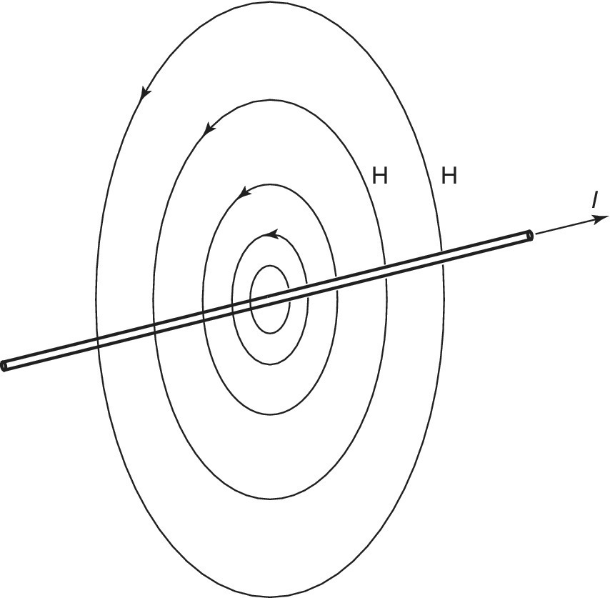
Figure 1.8 The magnetic field H around a current carrying conductor.
Ampere’s law states that the line integral of the H field around a conductor is equal to the current I in the conductor. In Figure 1.8, the H field is constant at a distance r from a long conductor which means that 2πrH = I. The magnetic field intensity H at a distance r from a long conductor carrying a current I is
where H has units of amperes per meter. Just like the electric field, the magnetic field shape is characterized by a set of curves. Just as in the E field, when the lines are close together, the field intensity is greatest.
An insulated conductor wound in a coil is called a solenoid. This arrangement is shown in Figure 1.9. The H field intensity in the center of the coil is nearly constant and it is proportional to the current and the number of turns. The field intensity in the coil is given approximately by
where I is the current in amperes, n is the number of turns, and ℓ is the length of the coil.

Figure 1.9 The H field in and around a solenoid.
There is no element of magnetic material that corresponds to the electron in the electric field. This means there is no magnetic pole that can be moved in the field to add energy. To understand the work required to establish a magnetic field, we need to discuss the concept of inductance and the induction or B field.
1.13 The B Field of Induction
In magnetics, we use an H field that is proportional to current flow and a B field that relates to induced voltage. This parallels the case in electrostatics where we described the electric field as a D field that originated on charges and as an E field that related to voltage. In electrostatics, the E field is the force field and in magnetics the B field is the induction or force field. In the electric field the presence of a dielectric reduces the E field and the energy density. In magnetics, the H field intensity is reduced in the presence of magnetic materials. Lines of force in the B field are called magnetic flux lines. The B field has units of teslas. B field intensity does not change at a boundary where the permeability changes. The H field is often called a magneto‐motive force. In a material with high permeability, it takes very little H field to establish a B field. In air, it takes a high magneto‐motive force to establish the B field.
When a changing B field flux couples to an open coil of wire, a voltage will appear at the ends of the coil. This is shown in Figure 1.10. A voltage can result if the coupled flux changes when an open coil is rotated or moved in the field. If the number of flux lines remains unchanged, the voltage is zero.

Figure 1.10 A voltage induced into a moving coil.
When there is a current there is an H field in space. At every point in space the H field has an associated B field given by
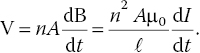
where μ0 is the permeability of free space and μR is the relative permeability. The value of μ0 is 4π × 10−7 Tm/A (tesla meters per ampere). This a fundamental constant in nature. The voltage induced in a coil is
where A is the area of the loop and n is the number of turns and dB/dt is the rate the B flux changes with time. This equation is known as Faraday’s law. This equation states that if the coupled induction field B changes intensity at a fixed rate, a steady voltage will appear at the coil ends. It also says that if a steady voltage is applied to the coil ends, the B field must increase linearly with time. This equation is true even if the coil is in air. Generally, at low frequencies, magnetic materials are used in the magnetic path to limit the magnetizing current needed to establish the B field.
In this book, we discuss the magnetic fields that surround traces carrying current. There will be no magnetic materials present, but there may be cross‐coupling between traces. Currents in traces will create an H field. Cross‐coupling between traces will involve the induction or B field. It will also turn out that the energy stored in a magnetic field involves both the B and H measure of the field.
1.14 Inductance
The definition of inductance is the ratio of magnetic flux to current flow or
As an example, the flux ϕ in a solenoid is equal approximately to the B field times the cross‐sectional area of the coil.
In general, exact equations of inductance using this definition are very difficult to generate. The inductance of a conductor geometry can be measured by noting the voltage that results when current changes value or
From this equation, it is obvious that every conductor geometry that can carry current generates magnetic flux and therefore has inductance. This includes the current flow in a capacitor. In circuit theory, magnetic fields are generally ignored. In transmission line theory, the magnetic field associated with a changing electric field is fundamental to moving energy.
Inductors are components that are designed to store magnetic field energy. At frequencies below a MHz, inductors usually require magnetic materials to direct the magnetic field to a volume of space called a gap. In later chapters, the inductance we consider involves traces running over plane conductors and involves no magnetic materials. The energy moved and stored in this inductance is key to logic operations.
There is magnetic field energy stored between a trace and a plane conductor when current flows in this loop. There is an electric field in this same space when a voltage is placed between the trace and a conducting plane. A trace over a conducting plane is thus a combination of an inductor and a capacitor. It is conventional to call this conductor geometry a transmission line.
The unit of inductance is the henry. Components that are intended to store magnetic field energy are called inductors. The inductance of typical components can range from microhenries (μH) to henries (H). When we study transmission lines, parallel conductors will have an inductance per unit length measured in nanohenries (nH).
Energy can be entered into an inductor by placing a voltage across its terminals. The power supplied at any moment is the product of voltage and current. The energy stored in the inductor is the integral of power over a time t. The energy is

Substituting Equation 1.23 for V

In Figure 1.7, when a constant voltage is applied to an inductor, the current ramps up in a linear manner. This is shown in Figure 1.11.
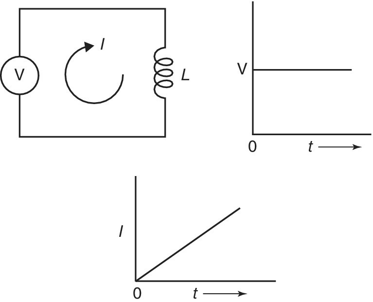
Figure 1.11 An inductor driven from a constant voltage source.
An isolated conductor has inductance. The magnetic flux generated by current flow depends on conductor length and only slightly on conductor diameter. Large diameters are required if high currents are involved. In a building, the I beams are in effect inductors that modify the fields that enter or are generated in the area. These fields are also modified by equipment racks, ground planes, conduit, and all metal surfaces. Attempting to reduce potential differences by “shorting” points together will usually fail. If an I beam did not affect the field, how can a no. 10 conductor be effective? The inductance of a length of round conductor is shown in Figure 1.12.

Figure 1.12 The inductance of round copper conductors.
1.15 Inductors
An inductor is a component that stores magnetic field energy. The inductors we consider later are made using trace geometries on a circuit board. These inductances are effective at high frequencies and usually do not involve magnetic materials. Inductances in the range 50 nH can be used to match transmission lines to a transmitting antenna at hundreds of MHz.
At lower frequencies, inductances can be supplied as components. These components can be turns of copper in air or turns wound around a magnetic core. When magnetic materials are involved, they shape the field but the energy is still stored mainly in air. In larger inductors, the magnetic flux crosses through air in a controlled gap. This is where the energy is stored.
A magnetic material in common use in circuit components is called ferrite. A ferrite core consists of small bits of magnetic material embedded in a ceramic filler that when fired forms a hard insulator. As an insulator, eddy current losses are limited to small islands of conductive material. Ferrite is the only magnetic material that has a useful relative permeability above 1 MHz. A typical gap structure is shown in Figure 1.13.

Figure 1.13 A magnetic circuit with an air gap.
Cup cores can be used to build an inductor. This core construction is shown in Figure 1.13. The core surfaces that touch are ground flat and polished. A controlled gap can be provided in the center of the core by grinding the center contacting surface. For transformer action, no gap is provided. This type of construction is shown in Figure 1.14.

Figure 1.14 Ferrite cup core construction.
A single turn threading a small ferrite bead forms an inductor. The reactance at 1 GHz is theoretically under an ohm and this assumes there is permeability at this frequency. Using a bead as a filter element to reduce noise is usually ineffective and is not recommended. The best approach in design is to avoid reflections, not add them. Often the role of the bead is to space conductors which reduce cross‐coupling. This can be done without adding a component.
1.16 The Inductance of a Solenoid in Air
A solenoid is a multiturn coil much like the symbol for inductor. The solenoids we are interested in consist of a few turns made from traces and vias. Magnetic materials are not considered as they are ineffective at the frequencies of interest.
From Equations 1.18 and 1.19, the B field in a solenoid is
From Equations 1.21 and 1.26
Referencing Equation 1.23, the self inductance of a solenoid is approximately

where A is the area of the coil, ℓ is the length of that coil, and n is the number of turns. The dimensions are in meters, μ0 = 4π × 10−7 tesla meters per ampere and the inductance is in henries.
An inductance of 10 nH has a theoretical reactance of 6.28 ohms at 100 MHz. It is not possible to build an inductor with zero parasitic capacitance. The natural frequency that results places an upper limit to what might be considered a simple inductor. It would be safe to say that at 1 GHz there are no simple components.
An imbedded inductor in the form of a solenoid can be formed on a circuit board using vias and traces. If the coil pitch is 15 mils where a single turn is 60 mils square, 10 turns will have an inductance of 76 nH. An increased pitch and more turns will help to increase the natural frequency.
1.17 Magnetic Field Energy Stored in Space
To calculate the magnetic field energy in a volume of space, consider a trace over a conducting plane as shown in Figure 1.15.

Figure 1.15 A trace over a conducting plane showing fields.
If the spacing h is small, most of the field energy will be stored in the volume under the trace. Ampere’s law requires that line integral of H around the current in the trace is equal to the current I. In this figure, most of the current flows out on the underside of the trace and returns under the dielectric on the conducting plane. Assuming that the only part of the path that contributes to the integral is along the width w under the trace,
If we assume H is uniform under the entire trace then
The magnetic B flux in an area hℓ is
Substituting Equations 1.22 and 1.28 into Equation 1.25, the energy in the magnetic field is
Since I = Hw, ϕ = Bℓh, and the product ℓhw is volume V, the energy in the field is
In magnetic material, the H field is very small and there is little energy storage. In a volume of space
1.18 Mutual Inductance
The current flowing in one conductor geometry can generate magnetic flux in a second conductor geometry. The ratio of this flux to the initial current is called a mutual inductance.
This changing flux can cross‐couple an interfering voltage into a nearby circuit. This coupling is most likely to happen when transmission lines run in parallel over a distance. Unlike mutual capacitance, mutual inductance can be of either polarity.
This coupling is discussed in Section 4.5.
1.19 Transformer Action
It is often very useful to generate multiple dc voltages to operate logic. Dc–dc converters can provide several voltage levels that can be referenced to points on a board. Converters are available as components.
One method of adding needed operating dc voltages uses transformer action. A square‐wave voltage is connected to a coil wound on a magnetic core without a gap. The voltage creates a steadily increasing B field. The B field intensity in iron depends only on voltage, the number of turns, the area of the core, and the time the voltage is connected. If a secondary coil is wound over the first coil, the magnetic flux will couple to this second coil. If the ratio of turns is 4 : 1, the voltage on the secondary coil is reduced by a factor of 4.
The magnetic flux in a core increases as long as a voltage is placed across a primary coil. When the flux level is near the permitted maximum, the voltage is reversed in polarity and the flux intensity starts to reduce. In time, the flux level goes through zero and reaches its negative limit. At this time the voltage polarity is again reversed. In a core with high relative permeability, the current that is needed to establish the H field is very small. This assumes there is no gap in the core. If a load is placed on the secondary coil the current that flows will obey Ohm’s law. The primary current will increase to supply the required energy into the load. The secondary voltages must be rectified, filtered, and regulated to serve as a dc power supply.
1.20 Poynting’s Vector
The idea that energy is moved in coupled electric and magnetic fields is fundamental in nature. The practical problem we face is that there are no direct tools for measuring energy flow or energy storage in space. The parameters we can measure are voltage, current, capacitance, and inductance. Poynting’s vector is a statement of power flow at a point in space using field parameters—not circuit parameters. This vector further presses the point that energy flows in space and that the conductors direct the path of energy flow. This vector is also valid in free space where there are no conductors. Figure 1.16 shows Poynting’s vector applied to a simple transmission line. The vector is mathematically the cross‐product of the E and H vectors or
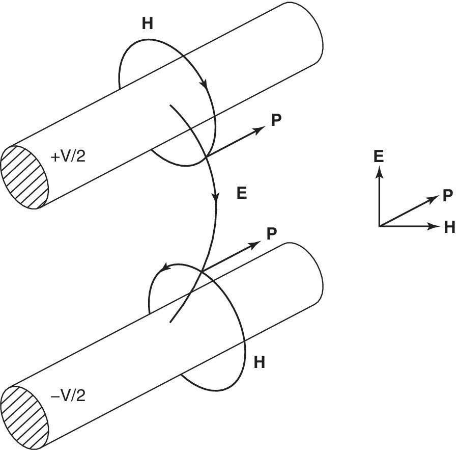
Figure 1.16 Poynting’s vector for parallel conductors carrying power.
The total power crossing an area is the integral of the Poynting’s vector component that is perpendicular to that area. It will be shown later that Poynting’s vector does not exist behind every wave front. Some waves convert field energy while others carry field energy.
Poynting’s vector has no frequency limits and applies to dc fields. The term dc implies an unchanging field in a region of space over a period of time. Utility power is carried in slowly changing fields in the space between conductors. A flashlight carries power from the battery to a lamp in space. A transmission line carries energy from a decoupling capacitor to a logic gate in the space between a trace and a ground plane. Space carries energy. Conductors direct where the energy travels.
1.21 Resistors and Resistance
Circuit theory is about resistors, capacitors, and inductors and how they function in networks at different frequencies. On a logic circuit board, resistors play a secondary role by terminating transmission lines. Resistance in a parasitic sense plays a role in dissipating the energy needed to move signals on these lines. This energy is dissipated in logic switches as well as in the traces that carry current. Initial currents stay on the surface of conductors. This effect means that most of the copper is not used and this raises the effective resistance. This is called skin effect and will be discussed later in the book.
The resistors that are used in analog work cover the range from 10 ohms to perhaps 100 megohms. All resistors have shunt parasitic capacitances of a few picofarads and the leads have an inductance of a few nanohenries. Circuit designers recognize these parasitic effects and design accordingly. In logic design, a typical impedance level is 50 ohms. This impedance is nominal whether the clock rate is 1 MHz or 1 GHz. This value is bounded above by the impedance of free space which is 377 ohms and the fact that it is impractical to work with 5‐ohm circuits. It is interesting that the geometric mean between 5 and 500 ohms is exactly 50 ohms. You may have noticed that over the years the characteristic impedance of transmission lines has remained constant even though clock rates have risen.
All resistors have a shunt parasitic capacitance. The shunt capacitance can be lowered by reducing the diameter and increasing the length of the resistor. Even the lead diameter must be considered. In this text, the resistors that are mentioned are ideal. To deal with a network that represents a practical resistor in a real environment is not useful. What is important is that compromise is necessary and being too idealistic will make it impossible to proceed.
The losses in conductors play a role in carrying a logic signal to its destination. If this resistance were zero, then the losses would be limited to the logic switches. As you will see, this energy cannot be saved or put back into the power supply. There is a good argument for limiting line losses as this maintains signal integrity. At the same time this puts a greater burden on the logic switches to dissipate this energy. A perfect switch cannot dissipate energy. Energy that is not dissipated or radiated must oscillate between storage in inductance and capacitance. All conductor geometries have capacitance and inductance.
The general engineering problem involves the resistance of conductors. If a trace is solder plated the surface resistance is raised and the losses increase. If a trace is silver plated the surface resistance drops and the losses drop. If a trace is treated with a conformal coating the current will use the copper. It is important to realize that there is no way to avoid dissipating energy. The resistivity ρ of various conductors is shown in Table 1.2. This table assumes the entire conductor is carrying current.
Table 1.2 The resistivity of common conductors.
| Conductor | Resistivity (μΩ cm) |
| Aluminum | 2.65 |
| Copper (annealed) | 1.772 |
| Gold (pure) | 2.44 |
| Iron | 10 |
| Lead | 22 |
| Nichrome | 100 |
| Platinum | 10 |
| Silver | 1.59 |
| Lead‐free solder | 12 |
| Tin | 11.5 |
The resistance of a conductor assuming an even flow of current is
where ℓ is the conductor length and A is the cross‐sectional area.
If the strip is a square where the width is equal to the length, the resistance is equal to
Thus, a square of material has the same resistance regardless of its size. The resistance in units of ohms‐per‐square depends only on thickness. This assumes that the current flow is uniform across the square and uses all the conducting material. The resistance does increase with frequency as skin effect limits the current penetration (see Section 2.17).
The resistance of copper and iron squares for moderate frequencies is shown in Table 1.3. This table is for sine waves, not step functions. Skin effect dominates the resistance for logic where most of the current flows on one surface.
Table 1.3 Ohms‐per‐square for copper and iron.
| Frequency | Copper | Steel | ||||
| t = 0.1 mm | t = 1 mm | t = 10 mm | t = 0.1 mm | t = 1 mm | t = 10 mm | |
| 10 Hz | 172 μΩ | 17.2 μΩ | 17.2 μΩ | 1.01 mΩ | 101 μΩ | 40.1 μΩ |
| 100 Hz | 172 μΩ | 17.2 μΩ | 3.35 μΩ | 1.01 mΩ | 128 μΩ | 126 μΩ |
| 1 kHz | 172 μΩ | 17.5 μΩ | 11.6 μΩ | 1.01 mΩ | 403 μΩ | 400 μΩ |
| 10 kHz | 172 μΩ | 33.5 μΩ | 36.9 μΩ | 1.28 mΩ | 1.26 mΩ | 1.26 mΩ |
| 100 kHz | 175 μΩ | 116 μΩ | 116 μΩ | 4.03 mΩ | 4.00 mΩ | 4.00 mΩ |
| 1 MHz | 335 μΩ | 369 μΩ | 369 μΩ | 12.6 mΩ | 12.6 mΩ | 12.6 mΩ |
| 10 MHz | 1.16 mΩ | 1.16 mΩ | 1.16 mΩ | 40.0 mΩ | 40.0 mΩ | 40.0 mΩ |
It is interesting to apply this table to a lightning pulse where the current flows uniformly across a square of copper. Assume the square has a resistance of 300 micro‐ohms per square. A current of 100,000 A would cause a voltage drop of 30 V. For a 0000 conductor the inductance of a 10‐foot section would be about 10 μH. The voltage drop for a lightning pulse would be about 4 million volts (see Figure 1.8). Connecting surfaces together using large diameter conductors is ineffective. To limit voltage drops, surfaces should be connected together so that current flow is not concentrated.
Problem Set
- 1 Assume a grain of sand is 0.1 mils in diameter. How many grains are there in a cubic foot?
- 2 Assume the current on a copper trace penetrates uniformly to a depth of 0.2 mils. What is the resistance per meter of a copper trace 5 mils wide?
- 3 A 50‐ohm resistor has a parasitic capacitance of 2 pF. What is the frequency where the reactance falls to 45 ohms? Use admittances.
- 4 The capacitance of a trace is 2 pF/cm. The relative dielectric constant is 4. What is the inductance per cm if the characteristic impedance is 50 ohms?
- 5 What is the current flow in a capacitance of 100 pF if the voltage across the capacitance changes 5 V in 2 ns?
- 6 The charge on an electron is 1.602 × 10⁻¹⁹ coulombs. How many electrons pass a point per second for a current of 100 mA?
- 7 Now many free electrons are in a gram of copper (about 1 cm of trace)?
- 8 Assuming only the top 0.01% of the copper contributes to current flow, what is the electron velocity?
- 9 What is the voltage across an inductor of 1 nH if the current rises 100 mA in 2 ns?
Glossary
- Ampere.
- A flow of charge at the rate of one coulomb per second. It is also the flow of displacement current represented by a changing D field.
- Ampere’s law.
- The H field around a long current carrying conductor is equal to I/2πr. The field lines are circles. The law stated in mathematical terms is: The line integral of H around any closed path is equal to the current passing through that loop (Section 1.12).
- Avogadro’s number.
- The number of atoms in a gram‐mole of any element. The number is 6.02 × 10²³. For copper the number of grams in a mole is 63.54 (Section 1.2).
- B field.
- The B field is the field of magnetic induction. The intensity of the field at a point is measured in teslas. A B field is represented by lines that form closed curves that do not change intensity when the permeability changes at a boundary. The B field is related to the H field by the equation B = μRμ0H, where μ0 is the permeability of free space, and μR is the relative permeability. μ0 is equal to 4π × 10−7 T/A m (Section 1.13).
- Capacitance.
- The ability of space to store electric field energy. In a capacitor it is the ratio of stored charge to voltage. The unit of capacitance is the farad (Section 1.7).
- Capacitor.
- A circuit component designed to store electric field energy (Section 1.8).
- Charge.
- A quantity of electrons gathered on a conductor or insulator. A coulomb of charge moving past a point per second is a current of one ampere (Section 1.2).
- Coulomb.
- The unit of charge. One coulomb per second is one ampere.
- D field.
- The electric field represented by charge distribution. The field lines are continuous across a dielectric boundary when there are no trapped electrons. The D field is proportional to the E field and is equal to ε0εRE (Section 1.9).
- Dielectric.
- An insulating material such as glass epoxy (Section 1.6).
- Dielectric constant (relative).
- The property of a material to reduce the electric field intensity (Section 1.7).
- Dielectric constant (permittivity).
- The constant that relates forces between charges. The permittivity of free space ε0 is 8.85 × 10⁻¹² F/m (Section 1.3).
- Displacement current.
- A changing electric field that is equivalent to a current and results in a magnetic field (Section 1.14).
- Displacement field.
- The D field (Section 1.9).
- E field.
- The force field that surrounds every charge. This is a vector field as it has intensity and direction at every point in space. Electric fields can attract or repel (Section 1.2).
- Electric field.
- See E field.
- Energy.
- The state of matter that allows work to be done.
- Farad.
- The unit of capacitance. The ratio of charge to voltage (Section 1.7).
- Faraday’s law.
- The voltage induced in a conducting loop by a changing magnetic flux (Section 1.13).
- Ferrite.
- A magnetic material in the form of a ceramic insulator.
- Flux.
- Fields are often represented by lines through points of equal intensity. These lines as a group are often called flux. It is common to refer to magnetic flux. Lines that are closer together represent a more intense field (Section 1.13).
- Force.
- That which changes the state of rest of matter.
- Force field (Electric).
- A state that attracts, repels, or accelerates charges.
- H field (static).
- The magnetic field associated with current flow. Magnetic fields are force fields that can attract or repel other magnetic fields. The H field is a vector field as it has intensity and direction at every point in space. The H field has units of amperes per meter (Section 1.12).
- Henry.
- The unit of inductance. Abbreviated as H (Section 1.14).
- Impedance.
- The opposition to current flow in a general circuit. For sine waves the real part is resistance, the imaginary part is reactance. Abbreviated as Z.
- Inductance.
- The ability of a space in or out of a component to store magnetic field energy. The correct definition of inductance is the amount of flux generated per unit of current. The unit of inductance is the henry. Abbreviated L (Section 1.14).
- Induction.
- The ability of a changing field to move charges on conductors or to create a potential difference in space (Section 1.13).
- Induction field.
- The magnetic or B field.
- Inductor.
- A component or conductor geometry that stores magnetic field energy (Section 1.15).
- Lines.
- A representation of field shape and intensity.
- Magnetic field.
- The force field surrounding current flow. The force field surrounding magnetized materials.
- Magneto‐motive force.
- The H field.
- Mho.
- An earlier unit of conductance. It is now the siemen.
- Mutual capacitance.
- Electric field coupling between different conductor geometries. Mutual capacitance is always negative (Section 1.10).
- Mutual inductance.
- Magnetic field coupling between different conductor geometries. Mutual inductance can be of either polarity (Section 1.18).
- Permeability.
- The ratio between the B and H magnetic field vectors. Abbreviated μ (Section 1.19).
- Permeability of free space.
- A fundamental constant. The relationship between the induction or B field and the H field in space. Referred to as μ0 (Section 1.13).
- Permittivity of free space.
- A fundamental constant. The relationship between the D and E fields in a vacuum. Referred to as ε0 (Section 1.9).
- Potential differences.
- Voltage differences between conductors or between points in space.
- Poynting’s vector.
- A vector formed by cross multiplying the electric and magnetic field vectors. The vector is equal to the intensity of power flowing perpendicular through an increment of area in space. The vector can be zero behind many wave fronts (Section 1.20).
- Reactance.
- The reciprocal of susceptance. The opposition to sinusoidal current flow in capacitors and inductors. In circuit theory the reactance of an inductor is a plus imaginary number of ohms. The reactance of a capacitor is a negative imaginary number of ohms.
- Resistance.
- The opposition to current flow. The real part of impedance.
- Self capacitance.
- The ratio of charge to voltage on the same conductor (Section 1.10).
- Self inductance.
- The ratio of the magnetic flux to current flow in the same conductor geometry (Section 1.16).
- Siemen.
- The unit of admittance. Reciprocal of impedance.
- Tesla.
- The unit of magnetic induction (B field) (Section 1.13).
- Transmission line.
- Parallel conductors that can direct the flow of energy.
- Vector.
- A line (and arrow) in space where length represents magnitude, intensity, and direction of a force field.
- Vector field.
- A parameter that varies both in intensity and direction in space. The most common fields are gravity, electric or E field, displacement or D field, magnetic or H field, and induction or B field.
- Voltage.
- Correctly, a voltage difference. The work required to move a unit charge a distance in an electric field. Measurements are usually measured between conductors. Voltage at a point in space has no meaning (Section 1.3).
- Work.
- Force times distance where the force direction is in line with the distance traveled (Section 1.3).
Answers to Problems
- 1 1.73 × 10¹⁵ grains in a cubic foot.
- 2 R = 0.274 ohms.
- 3 Use admittances. 782 MHz.
- 4 5 nH.
- 5 250 mA.
- 6 6.24 × 10¹⁷ electrons per second.
- 7 Avogadro’s number divided by 62.55 = 9.5 × 10²¹.
- 8 About 1 cm/second.
- 9 50 mA.