3
Transmission Lines—Part 2
3.1 Introduction
There is no polarity associated with field energy. One field does not cancel another. Consider the wakes of two boats on a lake. The waves will cross each other without any cancellation. Currents and voltages add and subtract in circuit theory and this represents one of the basic differences in how electrical phenomena is viewed. Another problem is that a rise in electric field intensity might occur while the magnetic field intensity is decreasing. This means that the term “rise time” must be used carefully. It would have been better to refer to transition time instead of rise time but that would defy convention. In the discussions that follow, it will be convenient to stress waveforms in terms of voltage. Keep in mind that there will usually be an associated current waveform present. These waveforms are drawn two‐dimensionally and what they represent are three‐dimensional fields. For traces on a circuit board the fields are usually cylindrical. When the path spreads out there are reflections and delays. This spreading of waves is three dimensional and not easily shown on the printed page. When there is spreading, there can be problems. The reader is asked to use his or her imagination to picture the wave action as outlined by the current path. The fact that the field lines are perpendicular to the direction of wave motion adds to the difficulty.
3.2 Energy Sources
Circuit boards can be operated from batteries, utility power, or even solar cells. In many cases the energy is supplied by an external power supply and brought to the circuit board on a cable or through a board‐edge connection. There is often an on‐board voltage regulator that conditions the voltage to the requirements of the circuitry. Converters are available that can supply different voltages. A shunt capacitor is often placed across active voltage sources to ensure stability and supply peaks of current if needed. The energy source we concentrate on is the simple decoupling capacitor. This capacitor is usually supplied energy over a transmission line from a nearby power supply.
The voltage that is switched onto transmission lines implies a supply of energy at the point of switching and this is the energy that is discussed in this section. In the analog world, wiring of a few inches to a regulated voltage would be entirely adequate. In logic, the problem is much more complex. It is important to accept the fact that initial current is controlled by the characteristic impedance of any connecting transmission lines. Fortunately, there are several immediate sources of energy near points of demand. This energy is stored in the capacitance of “connected” transmission lines.
A logic switch is usually a part of the die in the integrated circuit. In the die there may be other logic lines connected to the power potential through logic switches. Some of these lines extend through wiring to pads and out on to the board. Each of these connected paths is a transmission line storing electric field energy. In fact, many of these lines are physically no different than the lines that are usually labeled “power.” Energy taken from a connected logic trace introduces interference on that line. Nature pays no attention to the labels we attach to conductors. We, on the other hand, have to look beyond labels to see what is happening.
A second source of energy can be the capacitance between the power and ground planes if they are used. Drawing from this source of energy adds interference to logic using this same space. The third source of energy are any decoupling capacitors mounted on the board near the integrated circuit. If these local energy sources were not available, then a logic switch would connect two transmission lines together. One line might lead to a voltage source and one is a logic line. At this midpoint, the voltage would drop by about 50%. Because there are these local sources of energy, any drop in voltage is moderated. These sources of energy are shown in Figure 3.1.

Figure 3.1 The first energy sources when a logic trace is connected to the nearest power conductor.
3.3 The Ground Plane/Power Plane as an Energy Source
A limited amount of embedded energy is available from a ground/power plane pair. The capacitance is εRε0A/h, where A is the area and h is the spacing. The energy that flows into a central point from parallel conducting planes is pulled from concentric circles or rings. The characteristic impedance of a ring falls off inversely proportional to the radius. To increase the energy storage, a closer conductor spacing plus a higher dielectric constant is possible. The wave velocity falls off as the square root of the dielectric constant and this slows down access to this energy. The best way to increase the energy storage without adding delay is to decrease the conductor spacing. The characteristic impedance at the entry point will still be approximately 50 ohms. A single decoupling capacitor can outperform this energy source and provide a 3‐ohm source impedance. The economics are obvious. Accept any energy that is available but rely on decoupling capacitors as the principle energy source.
A power plane using the entire board is not recommended as traces using the ground/power space will couple to noise. Reducing the spacing between conducting planes makes it impractical to control the characteristic impedance of traces using this same space. At first glance, it seems like a good idea to make double use of this space. The problem is that space for logic transmission should be dedicated and the space used for energy storage must be shared.
3.4 What Is a Capacitor?
The simplest capacitors are formed by placing a dielectric between two conductors. The capacitance is a function of conductor area, dielectric thickness, and the dielectric constant. Small size is achieved by using thin dielectrics with high dielectric constants. For example, BST (Bismuth Strontium Titanate) can have dielectric constants as high as 12,000. The capacitance can vary with voltage and temperature, but these variations are not considered important in decoupling applications where the exact amount of stored energy is not important.
Capacitors are basic to all circuit design. They serve to block dc, to shape frequency responses, to reject noise, and to supply energy. On a board dedicated to processing logic, decoupling capacitors are the principle source of immediate energy.
We have already discussed the fact that it takes both inductance and capacitance to move energy along a transmission line. A capacitor has a series inductance that can be measured by observing its natural frequency. In circuit theory, this inductance might be considered a parasitic element. In logic, this inductance plus capacitance makes up a transmission line that can move energy. In circuit theory, the reactance of a stub depends on line length, frequency, the dielectric constant.2 In logic, the movement of energy from a capacitor is not defined by its stub parameters (reactances) but by the entire transmission path from the capacitor to the point of energy demand. The traces that connect the capacitor to a load are an impedance mismatch the flow of energy from the capacitor requires considerable wave action. The characteristic impedance of a capacitor at its terminals is about 3 ohms. If the rise time is long enough then wave action will not be apparent. Delays in moving energy are usually blamed on series inductance which is an over simplification.
In applications where a group of transmission lines carry parallel bit streams, the demand for energy can be high. Increasing the capacitance of a single decoupling capacitor will not usually support the step demands for more energy. A solution that is effective is to cluster a group of small capacitors at the integrated circuit. These parallel sources can provide the initial energy that no other conductor geometry can supply. An obvious help is to reduce the characteristic impedance of the line that connects the decoupling capacitors to the IC. If the characteristic impedance of the trace is reduced from 50 to 25 ohms, it will double the energy provided by each wave. The best solution is to mount capacitors at the IC pad and limit the transmission path to the die/pad distance.
3.5 Turning Corners
There is a sense that there is “mass and velocity” associated with any energy flow. This is a common feeling with no foundation. In Section 2.7, the point was made that the electric and magnetic fields behind a wave front are static and yet the coupled fields are carrying energy at the speed of light.
Many efforts have been made to detect reflections when a transmission line turns a right angle. Assumptions have been made that the traces should follow an arc or at least the sharp edges should be chamfered. There is no evidence that the wave action is affected by these efforts. This understanding must be extended to other minor transitions in transmission. It also applies to via transitions through board layers provided that the return current path is carefully controlled. Right‐angle transitions are not the problem. The spreading of fields is far more important. Another way to look at this type of transition is to notice the difference in path length as energy turns the corner. For a 5‐mil trace width the path length difference at the edges of the trace is only 5 mils. This is one wavelength at 2300 GHz. It is not surprising that we cannot see a reflection at a right‐angle bend.
3.6 Practical Transmissions
The intent in logic is to move energy from points of storage onto transmission lines. These transmission lines terminate on logic gates and the voltages at these gates will then control an action in an integrated circuit at a next clock time.
As we have shown, the first energy for a transmission comes from several sources (see Figure 3.1). The next level of complication relates to transitions in the characteristic impedance as waves progress back from the die to the voltage source and forward on a trace to a second pad and on IC wiring to a nearby logic gate. The voltage source in the following figure is ideal, but in practice it could be a decoupling capacitor with a 3‐ohm characteristic impedance.
In this figure, there are about 100 waves shown, most of them in the short wiring lengths in the ICs. These waves travel in the space between a conductor and an unspecified return path. The vertical axis is time (approximately). Note that the wave velocities vary depending on the dielectric constant and the transit time depends on the path length. The voltage at the open gate is the sum of all the waves that exit to the right on the diagram. The arrival time depends on the path taken. Obviously, the wave action continues beyond the 100 waves shown with ever‐decreasing wave amplitudes.
In Figure 3.1, it takes wave action to move energy inside an IC. This means that the total wave action is even more complex than the wave action shown in Figure 3.2. If all the transmission segments were 50 ohms, then there would be far fewer transitions. This example shows that higher bit rates will require more attention to detail both in IC packaging and on the board pad and trace structure. The reason is simple. All of this wave activity results in a delay in moving information. The energy is available but it is delayed as a result of wave action.

Figure 3.2 Wave action for a simple logic transmission. Note: Each wave is on a different time scale.
In Figure 3.2, a switch connected a logic line to 0 V and opened the connection to the supply voltage. The energy stored on the line begins to move. The wave action that follows must eventually dissipate the stored energy in switch and trace resistances. Some of this energy will be radiated. None of this energy can be returned to the source. This shows again that energy flow is a one‐way “downhill” path.
3.7 Radiation and Transmission Lines
Radiation in the form of a pulse can occur in nature. Examples are lightning, ESD, and solar flares. Step waves are the type of signals that radiate from transmission lines. Electrical engineering has methods of describing any electrical event in terms of its spectrum. Measurements are made by scanning the arriving field energy using narrow‐band filters. In the logic systems we consider, the signals have a frequency content that is determined by rise times and clock rates. Repetitive signals are characterized by signals at the fundamental clock rate and its harmonics. A single step function is characterized by a continuous spectrum with an upper frequency characterized as having a frequency of 1/πτR, where τR is the rise time. See the comments made in Appendix B.
At 1 MHz, a wavelength in space is 300 m. Unless a significant effort is made, circuits do not radiate very much energy at this low a frequency. A 100‐MHz square wave has frequency content well above 500 MHz and radiation efficiency increases as the square of frequency. This means that at this clock rate, the spectrum will allow for radiation. Errors in layout that invite board radiation are discussed in Chapter 5.
Many products in common use today function based on receiving radiation in the range 1 MHz to 10 GHz. Uncontrolled radiation could cause real problems for these products. For this reason, permitted levels of radiation are controlled by government regulations. A cell phone is expected to radiate but only over a controlled portion of the spectrum. Circuit boards intended for logic operations must pass strict radiation tests before they can be placed on the open market. These rules are important as the number of circuits in operation that radiate or receive radiation at any one time in an urban area can number in the thousands. The count is growing exponentially. The many circuit boards operating in a modern automobile is an example of the problem.
Coaxial transmission lines are used to confine fields. On a circuit board, transmission lines are not coaxial and some fields extend above surface traces and along trace edges. Regulations do allow for some radiation. Cables that enter a board can bring in field energy or provide a path for energy to leave the board.
Radiation is discussed in more detail in Chapter 5.
3.8 Multilayer Circuit Boards
Component density and pin counts on circuit boards have risen steadily. This, in turn, has resulted in the need for multilayer boards to accommodate the large number of interconnecting traces, most of which are transmission lines. Trace widths have dropped to accommodate larger trace counts and also to reduce board size. This need has reduced the diameter of drilled holes and made it more difficult to solder plate inner surfaces.
Board manufacturers can supply multilayer boards with layer counts over 60.
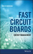
The manufacturing process involves plating and etching of copper layers separated by insulators. Many of the layers are laminates (cores) that are drilled and plated before being bonded together in a stack. Bonding a stack usually involves layers of partially cured epoxy called prepreg. Bonding of a layup takes place under pressure at an elevated temperature. A four‐layer board is made up of a core placed between sheets of prepreg and copper. Figure 3.3 shows a four‐layer board layup.
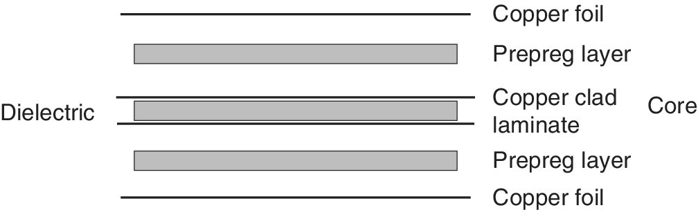
Figure 3.3 A four‐layer board layup.
There are several ways to assign functions to these layers. The core material is thick and separates the top two conducting layers from the bottom two conducting layers. This means that the outer logic layers are probably not going to cross‐couple. One arrangement assigns ground to the outer layers and logic and power to the inner layers. If power is distributed on traces then power planes are not required. A second arrangement assigns ground to the core conductors and logic and power to the outer layers. This has the advantage that traces make direct connections to components. These two arrangements are shown in Figure 3.4.
Figure 3.4 (a) and (b) Two four‐layer board configurations.
Six‐layer boards are built using the four‐layer structure with added layers of prepreg and copper on the top and bottom surfaces. The core laminate thickness is adjusted to control the overall board thickness. The conducting layers can be used for traces, ground planes, power planes, or a mix of these functions. There are good arguments for limiting power planes to the areas under large IC structures. The power space under an IC is apt to be noisy and any logic sharing this space will couple to this interference. Power connections can always be made using traces. This geometry controls fields and limits cross‐coupling. Figure 3.5 shows an acceptable layer assignment for a six‐layer board.

Figure 3.5 An acceptable six‐layer board configuration.
The core layers can be ground planes and all the remaining layers can be a mix of logic and ground or power planes.
3.9 Vias
Vias are plated holes that make electrical connections between conductors on different layers of a circuit board. It is common practice to connect a via to a pad at each conducting layer. Buried or embedded vias are not visible from the outside surfaces. Blind vias are visible from the outside surface but where the center holes are blocked by a conductor or plating.
The hole in a via is not a passage for fields. E field lines must terminate perpendicular to a conducting surface and can only exist if there is a potential difference. There is usually no potential difference across the walls of a small hollow conducting cylinder. It is safe to say that all wave activity and current flow involving vias will stay on their outer surfaces. Next, we treat trace transitions between layers using vias. These transitions are often a source of radiation.
3.10 Layer Crossings
When a logic line crosses between layers, the return path for current must be provided that controls the characteristic impedance. If this path is not provided, the field will spread out and the return current will use all available surfaces. The result will be reflection and radiation from the board edges. This problem is shown in Figure 3.6a. If a return path via is correctly positioned as in Figure 3.6b, this problem is significantly reduced.
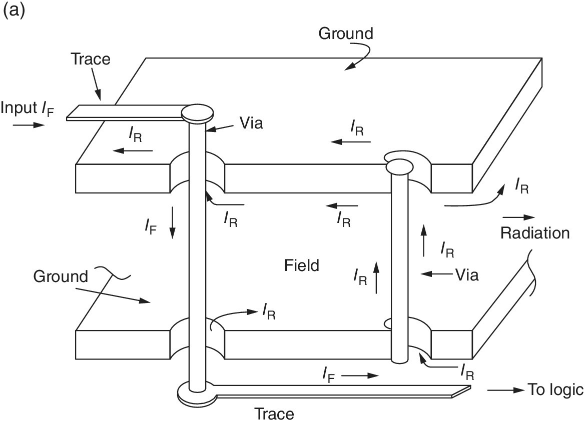
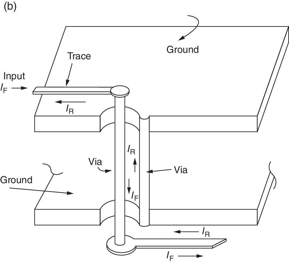
Figure 3.6 (a) A via crossing conducting planes with radiation and (b) Two vias crossing conducting planes.
The spacing between vias at a layer crossing controls the characteristic impedance of the transmission path. The characteristic impedance of parallel round conductors is

where d is the spacing between via centers and r is the radius of the via. If d/r = 2.2 and the relative dielectric constant is 3.5, the characteristic impedance will be 50 ohms.
3.11 Vias and Stripline
Stripline is a trace between two conducting planes. Field energy is carried in parallel paths. At the transition to and from the microstrip, vias are needed to merge the two field paths into one. If the transition is handled incorrectly, some of the field energy will not merge correctly and the result can be board edge radiation. The use of vias to merge the field is shown in Figure 3.7. As rise times shorten this merging problem becomes more critical.

Figure 3.7 Using vias in the transition from stripline to microstrip.
3.12 Stripline and the Power Plane
If stripline is placed between a ground and power plane, the merging of fields at the microstrip transition requires that the return current path use decoupling capacitors. This is a requirement at both ends of the stripline. Sharing decoupling capacitors can result in cross‐coupling. The current path is usually convoluted and this can result in reflections and delays. This is the further argument for using two ground planes in stripline transmissions. This return current path in a stripline transition is shown in Figure 3.8.
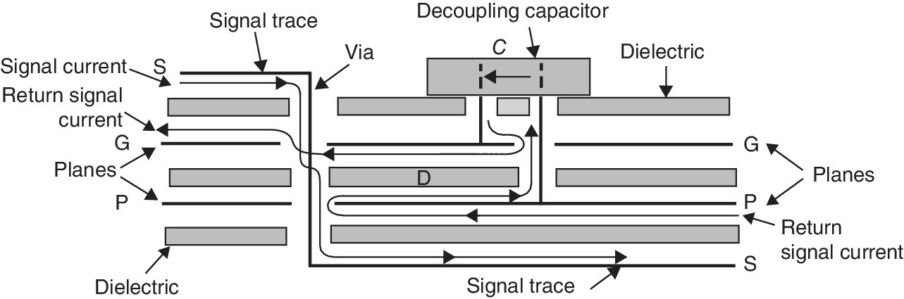
Figure 3.8 The return current path for stripline when a power plane is used.
For multilayer boards with many stripline traces, a lack of field control can result in very noisy transmissions and board edge radiation. As rise times shorten, the problem will only get worse.
3.13 Stubs
A stub is a branch transmission line usually of limited length. A stub is sometimes used to connect a logic signal to a second nearby location. If the stub length is less than two and a half times the rise‐time distance there will be little impact on transmission. Beyond this distance, the reflection at the junction will reduce the forward transmission to one third and many reflections are needed before the logic level is acceptable. The preferred method is to connect the two terminal points in tandem and avoid the stub. There might be a difference in arrival time but there will be no delay caused by multiple reflections. The delay caused by a midpoint stub is shown in Figure 3.9.
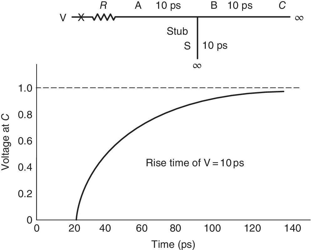
Figure 3.9 The delay caused by a stub on a transmission line.
The wave voltage after the matching resistor is V/2. When the forward wave reaches the stub, there are three waves: two forward waves and a reflected wave. Each forward wave has an amplitude of V/6. When a wave reaches the open end of the transmission line the voltage doubles to V/3. There are now three reflected waves returning toward the source. It will take several round trips and a dozen or more waves before the waves attenuate and a voltage of value near V reaches the two open ends. Without the stub, the arrival time is 20 ps. With the stub the arrival time is about 100 ps. If arrival time is critical then stubs are a mistake.
3.14 Traces and Ground (Power) Plane Breaks
If the return current for a transmission line must detour to get around a break in a ground plane, the break will act as a double stub and reflect energy. The only “fix” for this situation is a ground strap that completes the return current path near the trace crossing. A different layout is preferred. If the break is between a power and ground plane, a decoupling capacitor at the crossing point is needed but this situation should be avoided.
3.15 Characteristic Impedance of Traces
The control of characteristic impedance in a logic board layout is a focal point in design. In many layouts, trace lengths are short enough where terminating resistors are not required. A measure of characteristic impedance is still used to control manufacturing processes. It is an excellent quality control method that gives repeatability in both manufacturing and board performance. Controlling this one parameter does not guarantee that boards from different manufacturers will perform equally well.
There are several parameters that control characteristic impedance. For a microstrip, there are trace width and thickness, trace spacing, and dielectric constant. The manufacturer is limited in several ways. For example, trace thickness depends on available copper laminates that requires etching, plating, and cleaning. Spacings depend on the prepreg thicknesses that are available. The dielectric constant can vary with location depending on the grade of epoxy selected for cores and prepreg. This means that the board manufacturer must be consulted before parameters can be set. There are also economic considerations that must be considered. Smaller trace dimensions raise the cost of drilling holes and require tighter controls. The manufacturer must also allow for rejects in his pricing.
The following curves for different trace configurations are intended as a guide. Some of the configurations are rarely used and not all possible geometries are included. There are many computer programs available on the internet that can be used to calculate characteristic impedances. There are often variables that are not specified. Dielectrics can partially embed the trace. There are often conformal coatings that can affect the impedance. Since the dielectric constant varies with frequency, one number does not tell the full story. Step functions have a spectrum and this means that the leading edge can be affected in a nonlinear way.
The equations that are given below are approximations. Equations in the literature will vary depending on the accuracy desired and the range of the variables. The board manufacturer will have optimized his manufacturing techniques to control impedances. The curves are presented so that the reader can see how the characteristic impedance relates to various parameters. This information is not obvious by looking at the equations.
3.16 Microstrip
The traces on the outer layers of a logic board are called microstrips. The parameters for this trace geometry are shown in Figure 3.10.

Figure 3.10 Microstrip geometry.
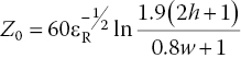
The characteristic impedance of a microstrip is given by Equation 3.1
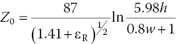
where 0.1 < w/h < 3 and where εR < 15.
There are several ways of presenting the relationship between parameters. Figures 3.11, 3.12, and 3.13 show the trace thicknesses of 1.5, 2, and 2.7 mils. In each figure, curves of characteristic impedance 40, 50, and 60 ohms are shown. The curves show that if all the dimensions are scaled, the characteristic impedance is nearly constant. The one parameter that is not controlled by the thickness of available materials is trace width.
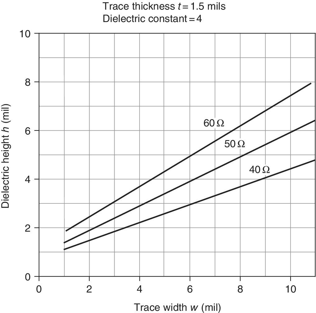
Figure 3.11 Microstrip parameters. Constant characteristic impedances for trace thickness of 1.5 mils.
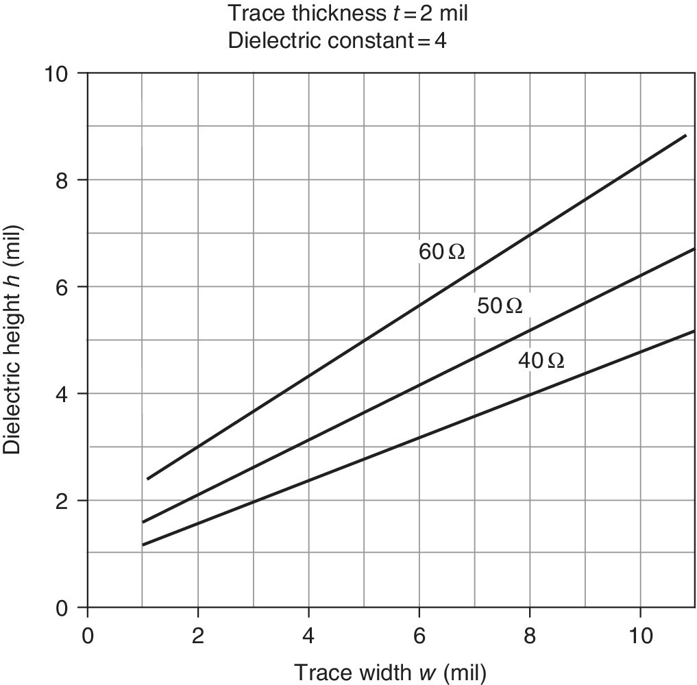
Figure 3.12 Microstrip parameters. Constant characteristic impedances for a trace thickness of 2 mils.

Figure 3.13 Microstrip parameters. Constant characteristic impedances for a trace thickness of 2.7 mils.
The parameters that are used for the embedded microstrip are shown in Figure 3.14.

Figure 3.14 Embedded microstrip geometry.
The equations for characteristic impedance for an embedded microstrip is given by
where h1 is >1.2h and εR < 15. The effective dielectric constant is given by

The benefit of an embedded microstrip is that surface currents for logic use the resistance of copper rather than the higher resistance of any solder plate.
3.17 Centered Stripline
Stripline refers to traces that are run between conducting planes. In centered stripline there are two paths for the energy flow. For a characteristic impedance of 50 ohms, each path has a characteristic impedance of 100 ohms.
Curves of constant characteristic impedance for a centered stripline for a trace thickness of 1.5 mils are shown in Figure 3.15.
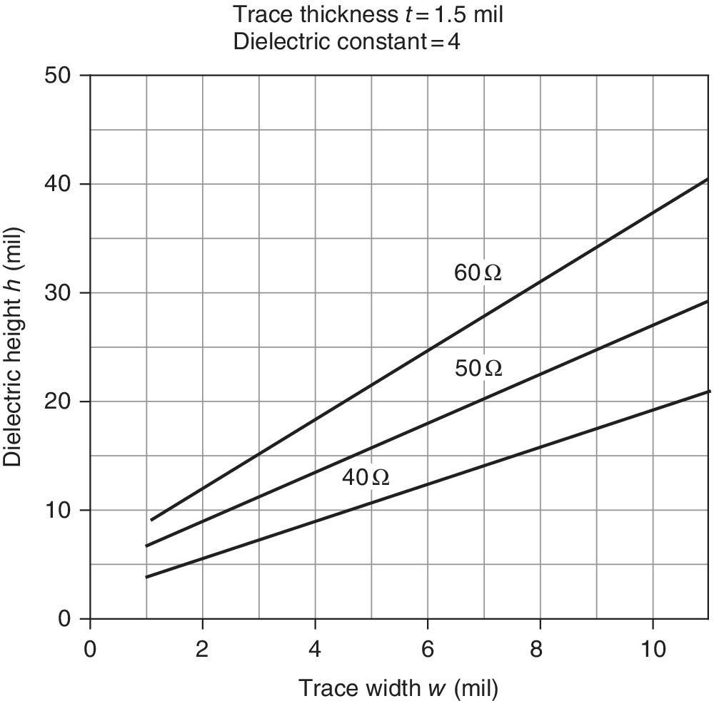
Figure 3.15 Centered stripline. Curves of constant characteristic impedance for a trace thickness of 1.5 mils.
The equation for characteristic impedance is
where 0.1 < w/h < 2, t/h < 0.25, and εR < 15.
3.18 Asymmetric Stripline
The parameters associated with an asymmetric stripline are shown in Figure 3.16.

Figure 3.16 Asymmetric stripline.
The equation for characteristic impedance is
where h1 > h, 0.1 < w/h < 2, and t/h < 2.5.
3.19 Two‐Layer Boards
It is practical to use a two‐sided board for fast logic. Ground and power planes are replaced by a grid of traces that carry both power and signal. Every logic line consists of three parallel traces called a triple. The triple consists of a logic trace between a ground and power trace in either order. The top of the board carries the triple in the x direction and the bottom of the board carries the triple in the y direction. Vias are used to transition the triple from the x to the y direction. On a 1/16‐inch board for a trace width of 10 mils, a trace separation of 10 mils, and a trace thickness of 2.7 mils, the characteristic impedance is about 50 ohms. Decoupling capacitors are placed across the triples at each IC. Care must be taken to add enough copper to feed power to the grid of triples. The grid supplies power and logic to each IC. A ring should connect all the grid ground and power traces together at each IC. Any board areas not used can be flooded with ground (see Figure 3.17).

Figure 3.17 Trace pattern for use on a two‐sided board.
3.20 Sine Waves on Transmission Lines
There are many applications where sine waves are processed on a circuit board. An application might involve a communications link. The role of characteristic impedance is somewhat different in these applications. In logic it was important to transfer a logic state in a short period of time. In a communications link, it is important to deliver a steady flow of sinusoidal energy to an antenna. What happens to the first cycles that reach the antenna can be ignored. The steady state energy that reaches the antenna is important.
Step waves gave us a unique understanding of how energy is managed on transmission lines. The effective handling of logic requires that reflections, if they occur, are handled correctly. In logic, one round trip should complete wave activity. An ideal transmission line has no losses. As we have seen, there can be step‐wave oscillations on a transmission line that is open or short circuited. Without resistance there is no way to lose the energy and it reflects back and forth. This means that an unterminated transmission line connected to a voltage generator cannot draw any real energy after the line is once energized. This is also true if the line is terminated in a capacitor, inductor, or any reactive network.
For a sine waves generator and an unterminated transmission line, there may be reactive energy flow where equal amounts of energy are added and subtracted on each cycle. This is exactly what happens when a sine wave voltage generator is placed across a capacitor or an inductor. A shorted or open transmission line looks like a capacitor or inductor that depends on line length and frequency. There are reflections at both ends of a line that obey the rules that were developed in the first chapters.
When a transmission line is used to carry sine wave energy to an antenna, reflections are not desired. The hope is that the arriving energy enters the antenna and radiates. Antennas must couple to the impedance of free space or 377 ohms and transmission lines on boards are typically 50 ohms. The problem of matching impedances and optimizing radiation is treated in Chapter 5. It is worth commenting that the impedance of free space is a resistance. Energy cannot be radiated into a reactance.
3.21 Shielded Cables
Shielded cables when used in microphones are a braid made from woven tinned small copper wires. This cable often carries conductors that supply power for preamplification. Wireless technology has largely replaced the standing microphone and the need for a cable. This technology has also replaced the cable connectors located at the receiving hardware. Power for the microphones is supplied from small batteries.
Instrumentation for strain gauges requires up to 10 conductors. Excitation and remote sensing takes up 4 lines, signal and calibration lines take up 5 lines, and the guard shield makes 10 conductors. The shielding for this cable is often aluminum foil that is anodized on the inside surface. The foil is folded along the cable and does not allow surface currents to circulate radially. A braided drain wire is run along the outside surface of the cable making it practical to terminate the foil at the cable ends. The shielding against interference fields below 100 kHz is excellent. For analog work, any rf coupled to the inner conductors can be filtered passively at the instrumentation.
Cables that connect piezoelectric transducers to signal conditioning must treat the triboelectric effect. In applications with a high ambient noise level, rubbing of the braid against the dielectric generates unwanted signals. Cables that limit this noise are available from transducer manufacturers.
3.22 Coax
The need to control the characteristic impedance in the transport of fields requires controlling the conductor geometry. Shielded cables that control the characteristic impedance are called coax. The geometry can be controlled by using a dielectric to center the inner conductor. The characteristic impedance of a coaxial transmission line with an air dielectric is shown in Figure 3.18.

Figure 3.18 The characteristic impedance of a coaxial geometry.
When a coaxial cable is needed for a transmission over any distance, the use of a dielectric allows a distributed reflection that is undesirable. To solve this problem, the inner conductor is centered by a spiraling nylon cord. The surface of braid also causes a distributed reflection. The preferred outer conductor is a thin smooth‐wall conductor that can flex. The copper center conductor is an alloy that will not easily bend or kink. A corrugated outer conductor can add flexibility but it adds to the distributed reflection and limits performance at high frequencies.
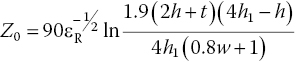
3.23 Transfer Impedance
Braided coax has a limitation that is caused by the conducting braid. Current on the inner surface will tend to follow individual strands of copper to the outer surface. In a like manner interfering external fields cause current flow to follow the individual strands into the cable. Any current on the inside surface is field and this is interference. This interference travels in both directions and appears as a voltage on the center conductor. This coupling can be reduced by using a double braid, but the added attenuation is not that useful.
The ratio between half the open‐end voltage and the shield current flow is called the transfer impedance of the cable. Figure 3.19 shows a typical terminated cable under test.
Figure 3.19 Transfer impedance test for a coaxial cable.
The transfer impedance for several cable types is shown in Figure 3.20. Note that thin wall at high frequencies provides excellent shielding where braid fails above 100 MHz. A transfer impedance of −40 dB ohms means that the transfer impedance is 0.01 ohms/m. A current of 1 A will develop an output voltage of 50 mV in 10 m of cable.
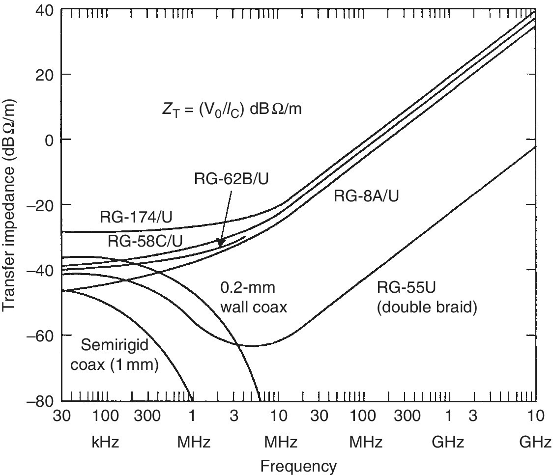
Figure 3.20 The transfer impedance for several standard cables.
The important thing to note is that the shielding of braided cable fails to be effective above about 300 MHz. For distances under 30 cm and frequencies under 1 GHz, the type of cable shield is usually unimportant.
The ideal termination of a shielded cable provides a smooth transition of interference current from the cable shield to the connector shell to the mounting surface. When the interference levels are severe, the best practice is to use backshell connectors. There must be a 360° shield termination without gaps. The connector body must be bonded electrically to the mounting enclosure preferably with a conducting gasket. For many applications where circuit boards are not enclosed, cable shields are used to control characteristic impedance not to limit interference. Closure does not necessarily control characteristic impedance.
Cables are often used to interconnect power supply leads, control leads, indicators, as well as logic. If any of these leads carry any interference current, then there is a good chance of cross‐coupling and the logic will be compromised. Here is a story that will illustrate this point.
I received a call from a friend on a Saturday morning. He had a piece of new hardware that had to be shipped. He had worked late the previous night, but had made no progress in solving an interference problem. This hardware measured oil flow and every time the pumps were operated there were errors. I got in my car and drove the 30 miles to see if I could help. He had connected a separate control panel to a computer using a shielded cable. I looked at the signal list and I found that he had added a conductor that connected the equipment ground of the control panel to the equipment ground of the computer. We cut this connection and the problem was solved. Normally transient effects would cause currents to flow on the outside cable shield. This added conductor brought the interfering field into the cable.
3.24 Waveguides
Transmitting high power at high frequency requires both a low characteristic impedance and a high voltage. In Figure 3.18, a low characteristic impedance in coax requires the spacing between conductors to be small. At a spacing of 5 mils, a 5‐V signal already has a voltage gradient of 1000 V/inch. This means that coax is not going to be effective for high‐power transmissions.
A waveguide is a hollow conducting cylinder like a rectangular air duct. At a frequency where one dimension of the opening is a half wavelength, sine wave electromagnetic energy will propagate along the cylinder without a center conductor. At specific higher frequencies, a waveguide will support propagation. A good example of this wave action is the operation of a microwave oven. A klystron supplies energy to a waveguide terminated in the oven compartment. The load in this case is the food in the oven. Without a center conductor, the field voltages in a waveguide can exceed 100,000 V/m. Waveguides are used in radar and in supplying energy to UHF transmitters.
As the frequency is raised the number of modes that can be carried on a microwave link increases until there is a continuum. The lowest frequency that can be transported is called the cutoff frequency. Driving the waveguide below this frequency is said to be driving the waveguide beyond cutoff.
The attenuation of wave energy beyond the cutoff frequency is given approximately by
where d is the largest aperture dimension, h is the aperture depth, and AWG is the wave attenuation in decibels.
A seam that is a few millimeters wide and 30 cm long will not be effective in shielding high‐frequency energy as AWG is unity. This is why a gasket is needed to seal the door on a microwave oven. The gasket must make ohmic contact with the entire seam so that surface currents can flow freely across the boundary.
FM radio operates on a carrier at about 100 MHz. The half wavelength is about 1.5 m. FM radio signals easily propagate into a road tunnel or an underground parking garage. An added conductor is needed to bring an AM signal into these same structures.
3.25 Balanced Lines
A balanced transmission line is a pair of conductors surrounded by a shield. Each conductor and the shield is a 50‐ohm line. The shield is a shared return path for two transmission lines. The term balanced means that the two transmission paths have the same characteristic impedance.
3.26 Circuit Board Materials
Board manufacturers have many choices in the glass epoxy used for board manufacture. Many forces have been at work to change board material. Increasing clock rates have brought on the need for a finer glass weave. Traces that by chance were located over a single glass ribbon would have a different characteristic impedance. One way to average the character of the weave is to use two layers of prepreg. This raises the cost but usually stabilizes the characteristic impedance. One of the biggest changes in board manufacturing occurred when lead was removed from solder. This directive is known as RoHS which stands for the Restriction of Hazardous Materials. Circuit boards must be cured at a higher temperature and this requires changes to the epoxy resin. Another problem is that smaller trace size requires more accurate drilling. Drilling and the use of thinner layers has increased the issue of mechanical stability. Many products require that boards be halogen free. If there is a fire, the gases that result could be lethal. Prepreg must match the mechanical properties of the copper laminates. All of this variability has made the problem of inventory difficult. It also leaves very little opportunity for a company to experiment with different materials.
Board manufacturers build products for many different users. Some users worry about dielectric losses while others worry about signal delays caused by variations in the dielectric constant. In most logic boards these are not critical parameters.
A board designer must be aware of these issues and should consult with board manufacturers so that a manufacturing specification can be agreed upon. As mentioned earlier, boards from different sources my not function the same way.
Problem Set
- 1 Describe the wave action when a voltage is switched onto a 100‐ohm transmission line in series with a 50‐ohm line.
- 2 A capacitor of 1 nF has a natural frequency of 100 MHz. What might the characteristic impedance be?
- 3 A 50‐ohm line connects to a 100‐ohm resistor. What is the reflection coefficient?
- 4 A 50‐ohm transmission line is charged at 10 V. A wave of 1 V is added to the line. What is energy in this wave? Assume the line length is 30 cm.
Glossary
- Balanced line
- Two conductors carrying odd mode logic. When one conductor is at logic 1, the other is at logic 0. The average value is kept at ½ (Section 3.25).
- Coax
- A shielded single conductor cable with a controlled geometry intended for high‐frequency applications (Section 3.22).
- Cross–coupling
- The unwanted transfer of energy between two controlled energy paths.
- Cutoff frequency
- The lowest frequency that can propagate on a waveguide (Section 3.24).
- Decoupling capacitor
- A capacitor in a logic circuit intended to supply local energy to transmission lines (Section 3.2).
- Die
- The core of a semiconductor product. A group of interconnected logic switches and semiconductor components usually made from silicon that performs a set of logic functions.
- Distributed reflection
- The reflection of wave energy along a cable. This reflection can result from irregular conducting surfaces or from variation in the dielectric constant (Section 3.22).
- Embedded energy
- The energy between conducting planes on a circuit board. The energy on transmission lines with a conducting plane as the return path (Section 3.3).
- Energy
- The state of a system that allows it to do work. Energy is stored in electric and magnetic fields. It is stored in a mass based on its position in a gravitational field. It is stored in a mass based on its velocity. A 5 V signal in transit on a 50‐ohm transmission line consumes ½ W of power. Energy is power times time. In 0.1 µs the energy moved is 0.5 × 10⁻⁷ joules (Section 3.2).
- ESD
- Electrostatic discharge.
- Glass epoxy
- The board material in common use in the manufacture of circuit boards. The term “glass” refers to a woven glass fabric used in the manufacture. The fineness of the glass mesh determines how constant the dielectric constant will be.
- Ground
- A conducting surface used as a local zero of potential. It can also be earth, power neutral, or a wire. The term has a very specific meaning in utility power.
- Ground plane
- A conducting surface on a circuit board at zero potential. The return current path for transmission lines (Section 3.3).
- IC
- Integrated circuit.
- Microstrip
- Traces on the outer surfaces of a circuit board (Section 3.16).
- Power
- The unit of power is watt. The rate at which energy is moved. A joule per second is 1 W. A 5‐V signal on a 50‐ohm line carries ½ W (Section 3.2).
- Power plane
- A conducting surface on a circuit board at the power supply potential (Section 3.3).
- Prepreg
- Sheets of partially cured glass epoxy used in board manufacture. Sheets of prepreg comes in many standard thicknesses (Section 3.8).
- Radiation
- The transfer of electromagnetic energy into free space (Section 3.7).
- Reactance
- The opposition to sinusoidal current flow in capacitance or inductance (Section 3.4).
- Return path
- In a transmission line, the path taken by current to return to the driving point. Vias provide both signal and return current paths.
- Shielding
- The use of conductors to contain an electric or magnetic field. Shielding can be a braid on a cable, a conductive housing, or a conductive layer in a transformer. It can also be a layer of magnetic material (Section 3.21).
- Stripline
- Traces located between conducting planes on a circuit board used as transmission lines. Centered lines are preferred as the energy is divided equally in two paths (Section 3.11).
- Stub
- A short transmission line usually connected to a main transmission line at some midpoint. A stub can be used to terminate a transmission line. Stubs can be terminated or used open or short circuited (Section 3.13).
- Transfer impedance
- The ratio of voltage coupled into a shielded cable from a current flowing on the shield’s outer surface. Because the coupled wave reflects and doubles at the open ends, the measured voltage is divided by 2 (Section 3.23).
- Vias
- Plated through holes on a circuit board that connect traces located on different conducting layers. Buried vias are not visible from the outer surface. Blind vias have the drilled holes filled with solder. Vias are supported by pads at each layer. Fields do not penetrate the holes associated with vias (Section 3.9).
- Waveguide
- Any hollow conducting cylinder that propagates electromagnetic energy without a center conductor. Usually used for sine wave propagation at high‐power levels at frequencies above 500 MHz (Section 3.24).
- Waveguide beyond cutoff
- A waveguide driven at a frequency that is too low to propagate energy.
Answers to Problems
- 1 The voltage V sets a wave in motion that reaches the 50‐ohm transition. The transmission coefficient is 0.667 V. The reflection coefficient is −0.333 V. When this wave reaches the voltage source the reflection reverses the polarity and a wave of +0.333 V moves forward. When this wave reaches the transition, two new waves are generated. The forward voltage thus increases in steps that reach V in the limit.
- 2 Assuming the entire capacitance resonates with the entire inductance, then fn = 1/6.28(LC)½. The inductance is 2.54 nH. Using this inductance the characteristic impedance is (L/C)½ = 1.2 ohms.
- 3 0.333.
- 4 A wave takes 1 ns to travel 30 cm. At 10 V and 50 ohms the power level is 2 W. The energy in a ns is 2 × 10⁻⁹ joules.