4
Interference
4.1 Introduction
Radiated interference can be roughly divided into two parts: energy that couples within a circuit and energy that enters from outside sources. Entering interference can come from radiation or cable connections. We discuss lightning and electrostatic discharge (ESD) separately.
This chapter deals with interference of all types and ways to limit its impact. Errors can occur in the sampling process. Utility power can be a source of interference when there are voltage surges, voltage dropouts, neutral voltage drops, and capacitive coupling. There can be instabilities in active circuits. Logic errors can occur when there are reflections, insufficient signal, or a lack of energy to carry the logic.
High‐speed logic requires greater bandwidth and this adds to the radiated levels. Reducing operating voltages limits radiation but makes circuits more susceptible to interference. The use of hard wires to carry signals through any distance has always been a problem. One difficulty is the coupling to interfering fields. The use of fiber optics and high‐frequency carrier links has eliminated many problems but this comes at a price. The data must first be put into a form where it can be transmitted.
We have already discussed two sources of interference generated on a circuit board: radiation from traces at the leading edges of waves and board edge radiation caused if fields are not provided a controlled space to use. The cross‐coupling of logic signals is another type of interference that is controlled by the layout. Cables that interconnect devices can couple to both local and remotely generated fields. This is nature taking every opportunity to spread energy out over any available conductor geometry.
When energy leaves the confines of transmission lines, the waveforms lose their step function character. The best way to measure and analyze this interfering is to use a sine wave analysis. The rise time character as discussed in Appendix B, shows that the frequency of interest for an analysis is given by 1/πτR where τR is the rise time or transition time. The approach that is taken is to assume that the interference can be represented by a sine wave signal at this rise‐time frequency and amplitude. The amplitude of the response using this one frequency represents the degree of coupling or interference. This approach can be used to estimate the effect impulses such as ESD or lightning can have on a circuit. This same approach can be used to estimate the impact logic signals will have in cross‐coupling.
As an example, an ESD event can be characterized as a 5‐A pulse. A typical pulse discharges field energy stored within a distance of 10 cm in about a nanosecond. The rise‐time frequency is about 300 MHz. A lightning pulse can be characterized as a 100,000‐A pulse. The field energy that is discharged and radiated is stored within a few hundred meters of the ionization path. The time for the initial energy to cross this distance is about 2 µs. The rise‐time frequency for this event is about 650 kHz. In both cases, the current level can be used to calculate an H field at a distance r. The B field in space is simply μ0H. The induced voltage in any nearby loop depends on the changing B field, the loop area, and the frequency (see Equations 1.16, 1.18, and 1.19).
4.2 Radiation—General Comments
Radiating structures (antennas) can be dipoles, loops, horns, slots, parabolic dishes, or arrays. Transmission lines and waveguides are used to carry energy from a circuit to these antennas for radiation. These same antennas can couple to fields that bring information into a circuit for processing. At 1 MHz, a transmitting antenna that is a quarter wavelength long is 75 m tall. At 300 MHz, a quarter wavelength in space is 25 cm. For practical reasons, receiving antennas are often much shorter than a quarter wavelength. The coupled voltage is roughly proportional to antenna length being optimum at a half wavelength.
A trace over a conducting plane forms a rectangular loop antenna that has a length equal to the distance traveled in one rise time. The field present along the rest of the trace is unchanging and it is therefore not radiating. The E field radiation at a distance of 1 m from a square centimeter of radiating area for a 1 V‐rms signal on a 50 line at 100 MHz is about 66 dBμV/m. This one example of radiation can be used to estimate the radiation from an entire circuit board. Radiating efficiency increases with the square of frequency. Field strength falls off linearly with distance. On a circuit board, the radiation that can be controlled comes from traces. Here the loop areas are small but the number of active loops can be in the hundreds. Radiation from board edges is usually the result of errors in the layout (see Sections 3.10 and 3.11).
Radiation levels from sources having the same spectrum are additive. Radiation levels from sources with a different spectrum are summed by taking the square root of their squared values. As an example, 30 mV of radiated carrier and 40 mV from a logic source will sum as (302 + 402)½ = 50 mV of interference. The sum can then be given in terms of decibels once a reference level is selected (see Appendix B).
4.3 The Impedance of Space
In Chapter 2, Equations 2.5 and 2.6 related the permeability and permittivity of free space to the ratio of current and voltage. It is easy to show that

where Z0 is called the characteristic impedance of free space. Using the values given in Section 2.5, this impedance is 377 ohms. This measure is also the ratio of the E and H field in an electromagnetic wave at a distance from a radiating source. Near the radiator, the wave impedance depends on the conductor geometry. For sine wave radiation, the distance λ traveled in one cycle is called a wavelength. The distance λ/2π is called the near‐field/far‐field interface distance. Beyond this distance, radiated waves are called far‐field waves. At 1 GHz, a wavelength is 30 cm and the interface distance is 4.7 cm. For a logic square‐wave signal, the interface distance is different for each harmonic. In the near field, coupling to nearby circuits will vary depending on the wave impedance of each harmonic. In the far field there is equal energy in the electric and magnetic fields.
4.4 Field Coupling to Open Parallel Conductors (Sine Waves)
Field coupling to a simple conductor geometry (wires) is shown in Figure 4.1. There are two things to note. Field coupling is optimum when the interfering field moves parallel to the path take by the conductors. The coupling is proportional to both path length and conductor spacing. Coupling is therefore proportional to loop area. The maximum distance that can be used in a calculation is the distance a wave travels in one clock time. For a larger dimension the coupling lessens but it is not a good idea to rely on any cancellation. The simplest way to reduce coupling is to reduce the coupling loop area. The interference fields can be from a nearby circuit board or from a remote source.

Figure 4.1 Field coupling to parallel conductors (wires).
In Figure 4.1, there are two field coupling areas. The first is the area between the two top conductors and the ground plane. In logic, voltage coupled into this area is called even‐mode interference. In circuit terminology, voltages that are coupled into this loop area are called common‐mode interference.
There can be field coupling to the area between a pair of conductors carrying a signal. In logic, this coupling is called odd‐mode interference. In circuit terminology, this is called normal‐mode interference. Depending on the cable type, this coupling can be reduced by twisting the conductors in the cable or by shielding.
4.5 Cross‐Coupling
There are designs that require long transmission paths where energy can cross‐couple causing interference. This section reviews the basic process so that a designer knows what to expect. There are many factors that should be considered including line lengths, trace proximity, logic direction, logic polarity, line terminations, rise time, and the logic family. Cross‐coupling is really the transfer of energy but the only coupling mechanisms we have discussed involve the E and H fields treated separately. We discuss coupling in terms of voltage as this is what we usually measure.
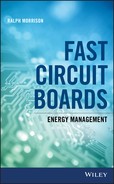
The circuit we consider is shown in Figure 4.2. The figure represents two transmission lines with mutual inductance L12 and mutual capacitance C12 per unit length.
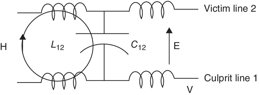
Figure 4.2 The mutual capacitance and mutual inductance between two transmission lines.
The two transmission lines are L1 (the culprit line) and L2 (the victim line). These lines are shown in Figure 4.3.

Figure 4.3 A step‐function wave applied to a culprit line.
As the culprit wave progresses to the right, the only area where the magnetic field couples to the victim is during the rise time. The coupled energy is restricted as the forward wave cannot exceed the speed of light. The coupled wave that moves to the left reaches a maximum amplitude in the distance traveled during the rise time. The rise time of the coupled energy is assumed to be twice that of the culprit rise time.
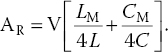
The wave component that results from inductive coupling is given approximately by
where L is the inductance per unit length in the two transmission lines and LM is the mutual inductance. The wave action described above is shown in Figure 4.4.
Figure 4.4 Inductive coupling between transmission lines.
The voltage component that results from capacitive coupling is similar to the inductive component. The total reverse‐coupled crosstalk wave amplitude is given by Equation 4.3, where C is the self capacitance and CM is the mutual capacitance per unit length.
4.6 Shielding—General Comments
In Chapter 1, the fundamental idea of shielding was introduced. Potential differences between conductors imply electric fields. If fields are fully contained by a conductor geometry, then the circuit generating this field is shielded. This basic idea leads to shielding methods that include metal enclosures, shielded cables, gaskets, and passive filters. The intent is to control which fields can leave or enter a controlled space. Power line filters on hardware allow utility power to enter but block high‐frequency energy. In general, line filters must be electrically outside but physically inside a metal enclosure. This requires the proper partitioning of space. Energy uses conductor pairs as transmission lines and nature pays no attention to labels. The NEC prohibits placing any component in the equipment grounding path, so this lead must remain electrically “outside” of any enclosure.
In the real world, circuits do not function in isolation. Even a cell phone must receive and radiate energy. Many circuits receive signals and operating energy using unfiltered conductors. All unfiltered conductors that enter a controlled space will bring in external field energy and provide a path for internal fields to exit the space. Field energy can enter and leave a controlled space through apertures and seams. The game that must be played is to limit the flow of interference energy and provide a clear path for desired energy. In analog work, the approach that is taken is to shield low‐level signals until they can be amplified and the impedance can be reduced to a few ohms. Active circuits can be used to reject any interference that is common‐mode. Out of band interference can be removed by passive filtering.
4.7 Even‐Mode Rejection
In logic, a signal often must be sent between boards or different pieces of hardware. It is expected that there will be a potential difference between circuit commons even if they are ohmically connected. The field in the intervening space will couple to all conductors that cross through this space. To limit this interference, a balanced signal can be generated in the transmitting logic. Both signals will couple to the same interference. The receiving circuit can amplify the difference in potential which eliminates the ground potential difference. This ground difference of potential is called even‐mode interference. The arriving signal is usually biased at the receiver so that it is unipolar. The ground difference of potential is called even‐mode interference.
In applications where balanced logic is used, the transmission distance requires terminations to avoid voltage doubling. The cable is usually a balanced 100‐ohm pair that ends on 50‐ohm lines on the receiving board. No terminating resistors are used at this point. The two signal lines are separated on the receiving board so that the two fields use a different space. At the receiving logic, two 50‐ohm terminating resistors are required. This circuitry is shown in Figure 4.5.
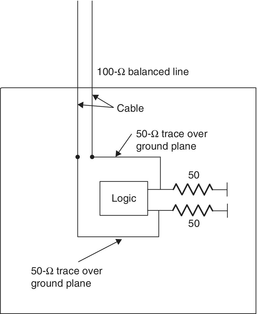
Figure 4.5 The termination of a balanced transmission line.
4.8 Ground—A General Discussion
In circuit board designs, the common or reference conductor at 0 V is often called ground. In many cases there is no earth connection. Obvious cases are cell phones and circuits in automobiles or aircraft. A ground can be as small as a postage stamp or as vast as an ocean.
There is often comfort in a concept that has no real basis: the idea that there is a “ground” that is quiet and that if we can connect to it, all noise problems will be conquered. The feeling is that the earth is a sump for noise. It can “absorb” the noise so that it will not reappear in a circuit. The circuit theory idea that current must flow in a loop is ignored. It is easy to find the entry point but the exit point(s) are a mystery. This feeling is so strong that significant attempts are often made to “ground” circuits to earth using tons of copper rods. The term quiet implies that the buildings will be noise free and will not allow radiation. Of course there is no physics to support this contention. Earth connections are important in power safety and in lightning protection. There are codes for the transport and grounding of utility power. The fact that these same conductors can function as transmission lines for rf energy is not considered. My trite remark is that nature does not read labels or color codes.
A bit of history will help explain a few common misconceptions. In the early days of electrification there were many cases where lightning entered a facility on power wiring. There were fires that resulted from a lack of fault protection and there were shock hazards. Under pressure from banking, insurance companies, and help from the National Fire Protection Agency, the National Electrical Code (NEC) was written and made a requirement in all electrical installations. This code is not a government regulation although it is adopted as a rule by most municipalities. The code defines the meaning of key words. I have, in a few cases, indicated these words in italics. The code is amended every 3 years to accommodate new practices and new materials. The latest code is dated 2017. The code provides rules and makes no attempt at any analysis. The code requires that utility power be connected to earth at the service entrance at each facility. The assumption is that lightning that strikes utility conductors will flow to earth outside of a facility. This rule applies to underground power entrances. It is important that all facilities should obey the same rules. Not all countries follow these same grounding rules. On board naval ships, power is ungrounded. In some areas on a ship, a distribution transformer is added and the secondary is grounded. Floating the power system reduces electrolysis problems and allows for faults in combat that could disable key equipment. Unfortunately when power is floating, any changes in power demand produces interference that propagates over the entire power system even if it is in conduit.
Many facilities on the same utility line make neutral connections to earth. In three‐phase distribution, the phase loads are not exactly balanced. This means that some neutral current uses the earth as a return conductor. Some of this current in turn uses gas, water, and telephone lines as well as building steel. As pointed out, this current only flows because there are fields. The utility has no legal obligation to reduce this current. Generating this current requires capital equipment and balancing loads is in the right direction. The utilities cannot completely control this balancing.
Electronics has evolved in the presence of utility power. Early circuits used vacuum tubes which meant power transformers and relatively high voltages. Any engineer designing hardware learned very quickly that shields were needed around signal conductors or that the coupling to electric fields from utility power will be a problem. It was noted that if the mounting hardware is connected to earth, the coupling is reduced. This in turn led to the idea of providing a dedicated ground to be used for signals, shields, and racks containing electronics. This idea of a single‐point ground for all electronics became law in defense installations. The code was changed to allow equipment grounding conductors (green wires) to be ungrounded (isolated) at the receptacle and grounded at the service entrance. There are many installations where this grounding procedure has introduced significant noise problems. The practice is no longer allowed in hospitals as there is an added risk rather than an added safety factor. Obviously, there are many wiring methods that are safe. Not all of the methods are compatible with noise control. The role of engineering is to choose the method that fits the need.
Efforts to provide separate equipment grounds for parts of a facility are unsafe as some faults could go undetected.1 The code will permit floating power but only when there is a specific need and where there can be close supervision. Examples are some assembly lines and electrically heated crucibles. A fault detection system must be provided.
The word ground has many meanings to engineers. It has many nontechnical meanings as well. It is a word that seems to attract many uses. The National Electrical Code provides definitions that are quite clear. This code is law in most cities. For example, the grounded conductor is the current‐carrying power conductor that is connected to earth at a service entrance. It is colored white. Equipment grounding conductors cannot be used for carrying power current and they are colored green or it can be a bare copper wire. No other power conductor can be colored green. Any conductor that could come in touch with a power conductor is called an equipment ground. This includes racks, metal cabinets, motors, generators, and power transformers. All equipment grounds are connected together and are earthed at the service entrance. Any electrical hardware that uses utility power that could be a source of electrical shock must be grounded per code. The code establishes grounding rules that guarantees that any fault current path will be low impedance so that a breaker will trip if there is a fault. All equipment used to carry power wiring must be listed. This means it has passed tests that guarantee performance over time in all types of weather. It is illegal to modify or tamper with listed hardware.
Ground becomes an issue in the desert. In the summer, the earth’s surface is an insulator. It is impractical to seek a conducting layer by drilling down hundreds of feet. The same thing happens on lava beds or on granite outcroppings. An earth connection can be impractical. There can still be lightning strikes and fault conditions that can be dangerous. The general rule is that all common conductors that a human can touch should be bonded together forming a grid. There are thunder storms in the desert and this can damage distribution transformers using isolated grounds. Lightning can strike a jet aircraft but as long as it is one conducting surface no damage will result. Two comments: Lightning currents must not enter an area where fuel vapor can be ignited. At the base of towers, the current must be dispersed over the earth’s surface so that there are no points of concentration in the structure. Concentration of current can melt metal and topple a structure.
The earth as a conductor has conductivity that varies over a wide range. Skin effect is dominant when the surface is damp and current will flow on the surface. A nearby lightning strike will electrocute cattle standing on wet soil. The ocean is a good conductor and the current from a lightning strike will stay on the ocean surface. This is skin effect. A strike to a ship will not enter the water much below the water line. This has implications in providing current paths in lightning protection. For example, on a boat, current will not use the keel to enter the water. It may arc through an insulated hull at the water line.
In circuit board designs the common or reference conductor at 0 V is often called ground. In many circuits there is no earth connection. Obvious cases are cell phones and installations in automobiles or aircraft and of course, satellites.
4.9 Grounds on Circuit Boards
The ground plane used in a logic structure is a convenient way to form transmission lines. A separate return conductor for each transmission line would also function but it takes more etching and this reduces mechanical stability. Engineers often try to make measurements of voltage drops along a transmission line. The voltage at the ends of the transmission line is available on pads but the voltage at midpoints on traces requires cutting through any conformal coat or dielectric. There are several comments that might be helpful. A voltage measurement is really a field measure and the field being measured can originate from nearby sources. The presence of a probe can change the amplitude of the field so that the measure may be invalid. Here are two precautions to take. Connect the tip of the probe to the probe common. Make sure there is no signal when the probe is near the board. Connect the shorted probe to the board common to make sure there is no signal. If there is signal there may be current flow in the probe shield that is coupling field into the input. This would indicate that a better probe is needed.
A question often arises as to how to connect a circuit board to a conducting enclosure. If the circuit board receives data over a cable then an added ground might allow fields a second transmission line path that uses the ground plane of the circuit board. This is an example of where a single‐point ground is preferred. The board should be grounded so that any field that uses this added transmission line does not use the board ground plane as one of its conductors. If interfering fields terminate on the ground plane it could add interference. Stated another way, the ground connection should not form a current path so that interference currents flow on the ground plane.
4.10 Equipment Ground
Hardware that is rack mounted usually makes use of utility power. The National Electrical Code requires that the rack and all hardware mounted to it be treated as equipment and grounded per code. Power line filters use the equipment ground as a return conductor. The current flow can result from activity in the hardware or coupled to the power conductors from other hardware. In large systems, these line filters can place a significant reactive load on the line. The fields associated with this filtering are not totally confined and can contribute to the general ambient field in a facility. The ambient noise field intensity will be reduced if this current is provided many parallel paths to follow. This is the reason that isolated equipment grounds are not effective. An example will illustrate the problem. Two computers are coupled together. Each is powered using an isolated ground. A nearby elevator motor creates a transient field that couples field energy to the equipment ground loop. The logic connection is closure for the equipment ground loop and the induced voltage transient blows up circuitry at the interface. Rather than reduce interference, the isolated grounds created problems. If the computers were coupled using an rf link or fiber optics, this would not occur. The less costly solution is to connect all equipment grounds together in a grid.
4.11 Guard Shields
In analog instrumentation, signals are often in the millivolts. To maintain signal integrity, all errors of 0.1% or greater must be considered. There are literally dozens of mechanisms that can contribute errors at this level. One major problem is the ground difference of potential between the signal source common and the instrumentation output common. This potential difference can often exceed 10 V. For a 10‐mV signal with a source impedance of 1000 ohms, the error voltage is limited to 10 μV. For a 10‐V common‐mode signal, the error current level is limited to 10−8 A. This is an input impedance of 1000 megohms. At 60 Hz this is a leakage capacitance of 2.7 pF. This is a difficult restraint on both the signal cable and on the instrument design. These figures are presented to show why it is desirable to avoid this approach to analog signal processing.
The potential difference between grounds is a measure of the field intensity in the intervening space between a source transducer and any signal processing. The ground difference in potential is called common‐mode interference. The arriving shield is called a guard shield and it guards the signal conductors up to the input integrated circuit pads. This shield is grounded at the transducer and not connected to the local common. A simplified schematic of this circuit arrangement is shown in Figure 4.6.

Figure 4.6 A differential amplifier using a guard shield.
Filters and clamping circuits protect the input against any overvoltage that might occur. The guard shield is not expected to be effective above 100 kHz. The guard shield is connected to local common above this frequency. A typical connection is a 0.01 μF capacitor in series with 100 ohms. If the input shield were to be grounded to the local common there would be a voltage gradient along the shield and this would couple interference directly into the signal path. Transient common‐mode signals can often exceed 100 V.2 In practical applications, rejection ratios must exceed a million to one at frequencies of 100 Hz. This requires the amplifier input impedance Z1 and Z2 must be 1000 megohms. This problem is avoided if the signal is amplified, digitized, and carried by fields to a remote point for processing and data storage. The field can use free space or fiber optics but not a hard wire connection.
4.12 Forward Referencing Amplifiers
Analog signals that are preconditioned must often be brought to a logic board for processing. The signals are often carried on a single coax cable. The signal level can be bipolar and limited to ±5 V. The source impedance is usually under 1 ohm and the bandwidth can be as high as 100 kHz. The basic problem is that the reference conductor is at a different potential than the logic board reference conductor. Connecting the two reference conductors together invites current flow that can result in interference. The interference can impact the analog signal and in some instances it can impact the logic.
A simple differential amplifier with unity gain can buffer the signal and limit the common current flow to a few milliamperes. The common of the analog signal can be connected to either of the differential inputs depending on the desired gain polarity. The two commons are not connected together. The circuit arrangement is shown in Figure 4.7. This circuit would normally require a negative power supply voltage. This circuit is not intended for terminating a transmission line. The use of 50‐ohm feedback resistors would require current levels of 100 mA. Thousand‐ohm resistors are usually very effective. Typically, analog IC amplifiers have limited current capability.

Figure 4.7 A forward referencing amplifier.
4.13 A/D Converters
The interface between an analog signal and an A/D converter on a logic board presents a unique problem. The analog signal is referenced to a remote source ground. The A/D converter is referenced to logic common. The input to the A/D converter is usually a forward reference amplifier similar to the one used in Figure 4.5.
An A/D converter might have 12‐bit resolution which means that the interference level must be below 1 mV. It is important not to couple normal‐mode interference to the signal path. If the signal common is grounded, current flowing in this conductor can easily add normal‐mode interference that cannot be rejected by the forward referencing amplifier. The best practice is to separate analog signal space from logic signal space. There can be only one common conductor. The analog space must use dedicated pins, traces, and power connections. The analog input signal loop must have minimum area. Any attempt to use separate grounds will only increase the interference coupling.
4.14 Utility Transformers and Interference
Utility power plays an important role in moving both energy and interference throughout a facility. In industry, utility power runs computers, lights, elevators, assembly lines, and communications systems. There are many opportunities for interference in the form of field generation and transmission through the utility lines. Transformers in individual devices allow the power source to be referenced to many different common points. The transformers in each device provide a path for interference to travel in both directions. In many products, energy is transferred using dc‐to‐dc converters which can add a pulse‐like character to the interference.
The electrical code allows for only one grounding grid in a facility. The code allows for separately derived sources of power and for separate distribution transformers, but for safety there can be only one grounding system. Power supplied from a backup generator or from an added transformer is said to be separately derived. The neutral and all equipment grounds are brought back to each power source and earthed to the nearest available point. The important point is that power from a separately derived transformer allows the use of a dedicated neutral. The voltage drops in a shared neutral can often be a source of interference. The neutral or grounded power conductor can connect to earth and the equipment ground only once and that is at the service entrance. Each source of power is treated as a service entrance.
Utility power is usually generated three phase. The coils that rotate in a magnetic field that generate the voltage are spaced 120° apart. The reason for three‐phase power relates to the torque on the rotor. If the phase loads are balanced the torque on the rotor is constant over every revolution. Without a fixed torque, vibrations would tear up the shaft bearings in a very short period of time.
Distribution transformers for a building are sometimes centrally located to reduce cost. The leakage magnetic field near the transformer can be a source of interference. This field is proportional to secondary load current that can be quite high. In installations of this type the limit of magnetic field strength at full load should be specified. Attempts to shield this type of interference are usually not successful.
Distribution transformers should not be mounted where leakage fields can couple current into the building steel. Nearby conducting loops should be broken by using insulators.
4.15 Shielding of Distribution Power Transformers
In facilities where power is used for industrial activities, there can be electrical interference carried on the power conductors. There are many levels to interference including power surges, voltage sags, spikes, and high‐frequency transmissions. Power conductors are transmission lines that can carry interference for long distances. In critical installations, a shielded distribution transformer can be used to service specific hardware. Internal to the distribution transformer there can be three shields. These shields consist of three conducting layers of either copper or aluminum that surround the primary coils of the transformer. The shields must not form shorted turns around the iron core. The purpose of the shields is to control the paths taken by interfering reactive currents. The primary coil is usually wound next to the core.
The first or primary shield is placed over the primary coil. It is connected to the end coil of the primary winding. The center shield is connected to the equipment ground or metal frame around the transformer. The third shield is connected to the start of the secondary coil.
The center shield is the common‐mode shield. It blocks the flow of common‐mode currents on the primary conductors from flowing in the secondary circuit through coil‐to‐coil capacitance. The primary and secondary shields keep common‐mode currents from flowing in leakage capacitance to the coils of the transformer which can then enter the secondary circuits by transformer action.
In a three‐phase transformer, each of the three legs are separately shielded. All shields are connected inside the transformer. This shielding is shown in Figure 4.8.
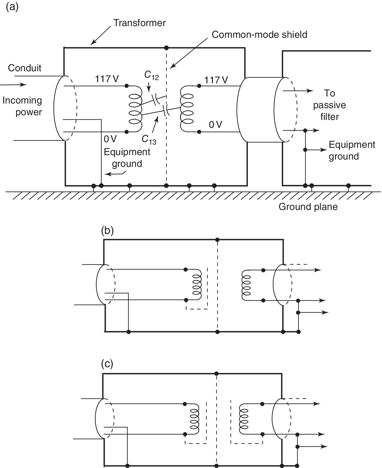
Figure 4.8 A single‐phase isolation transformer. (a) One shield, (b) two shields, and (c) three shields.
4.16 Electrostatic Discharge
There are many situations that can cause charges to accumulate on an insulated body. The friction of shoes on a rug or on floor tiles can build up a charge on a human body. Charges can build up on an insulated chute carrying moving grain. The discharge of this energy can start fires or cause explosions. An aircraft in flight can build up a charge moving through air. Fueling of aircraft requires careful grounding procedures so that arcing does not occur around fueling. Charges can build up on an insulated bag when integrated circuits are removed. This arcing can damage semiconductors. If a discharge takes place on a cell phone or on a keypad, there must not be damage to circuitry. Manufacturers must test their hardware to make sure that it can survive ESD pulses. In the manufacture of integrated circuits, humidity is controlled and there are clothing restrictions. Low‐voltage arcing can produce problems that can go undetected. In computer installations, floor tiles are made slightly conductive so that any charge buildup is immediately discharged. This means that each tile must be correctly grounded. Grounding clips must be replaced if removed. Rotating floor polishers are not allowed.
Humidity control in a facility is the best way to limit ESD problems. Adding humidifiers is not always effective as there can be areas that do not get treated air.
All products that contain electronics should be tested to make sure they are not damaged by ESD. Performance in the presence of ESD is usually not expected. Any external conductors that provide an electrical path into the electronics should be tested. This includes power and signal cables. Devices that are grounded through a power cord are more vulnerable than devices that are battery operated. The issue is: Where will the arcing take place and what is the current path? These two factors define where the interference field is located and what the field intensity will be at points of difficulty. Energy can enter through apertures, seams, or pins on open connectors. Energy can enter on shields that are not properly terminated, power leads that are not properly filtered, and through displays. A control that is mounted on a painted or anodized surface can provide an ESD entrance.
An ESD current pulse creates a significant magnetic field that can couple into any nearby loop area. If the current spreads out over a conductive surface, the field intensity is significantly reduced. Providing multiple current paths for the current is obviously in the right direction. Single‐point connections concentrate current flow and this in turn increases field intensity.
Commercial zappers are available for testing hardware that generate controlled pulses of current. The voltage that initiates the pulse can be varied from 1,000 to 15,000 V. The current level is typically 5 A. An ESD pulse can be characterized as being a sine wave current at a frequency of 300 MHz. The pulses can be single or repeated events. There are two basic modes of testing. One mode is where the probe makes ohmic contact and there is no probe tip arcing and the second mode is when the probe arcs to the device under test.
An example of coupling provides some insight into the nature of the problem. Consider an ESD pulse of 5 A. Using Equation 1.16, the H field at a distance of 10 cm is I/2πr = 79 A/m. Using Equation 1.18, B = μ0H = 10−4 teslas. Consider a loop of 1.0 cm2 coupling to this field. Using Equation 1.19 at a frequency of 300 MHz, the voltage induced in this loop is 19 V. This voltage will destroy an integrated circuit. The current pulse does not need to flow in a component to do damage.
A problem exists when the device being tested is not grounded. Repeated zapping can build up a stored charge that may eventually cause a breakdown that would not normally occur. If this condition exists, a discharge path using a 100‐megohm resistor can be added. Devices that use a power adapter can be vulnerable when the voltage buildup can arc across the power coils in a transformer. The buildup of static charge limits the voltage difference to the zapper and this can invalidate the test.
Testing should proceed at selected intermediate voltages. High voltage arcs lose a lot of energy to heat. The most critical voltage is often at about 7000 V.
4.17 Aliasing Errors
An example of an aliasing error occurs in old Western motion pictures where wagon wheels appear to rotate backward. To avoid this error the data must be sampled and displayed at a higher rate. The rule is that data should be filtered and then sampled more than two and a half times the highest frequency of interest. If the data is temperature, it is easy to assume that sampling at a high frequency is unnecessary. The problem that exists is that there may be interference mixed with the signal and sampling this interference can result in a measurement that looks like temperature. The accepted way to avoid this problem is to filter the data before sampling. Filtering should not be done digitally after sampling as there may be aliasing errors. Filtering data in the analog domain is expensive but often it is necessary.
If the sampling rate of the wagon wheels is slowed, the reverse wheel rotation rate will appear to increase. This apparent shift in spectrum can be used as a test to determine if an aliasing error has occurred. With the enormous capacity we have for storing and processing data, a simple spectral analysis is very practical. The data is analyzed at two noninteger sample rates. If the spectrum shifts linearly the data is invalid.
Glossary
- Aliasing error
- A sampling error that results when data contains frequency content close to the sampling rate (Section 4.17).
- Cross‐coupling
- The unwanted transfer of energy between circuits. This is often the energy transferred between transmission lines. Long transmission lines are the most vulnerable. The victim wave travels in the opposite direction to the culprit wave.
- Equipment ground
- All conductors that could contact a utility power conductor. These conductors include racks, cabinets, housings, junction boxes, conduit, raceways, generators, motors, breakers, and so forth. Equipment ground conductors are green or solid wires running next to current‐carrying conductors to keep the fault paths low impedance. They connect to the neutral conductor at one point in the service entrance. Equipment grounds can be earthed at multiple points.
- Electrostatic discharge (ESD)
- The high‐voltage phenomena where friction moves charges so that they accumulate on bodies and arc when the breakdown potential is reached (Section 4.16).
- Even‐mode coupling
- Coupling that adds to a logic signal and impacts signal integrity (Section 4.7).
- Forward referencing amplifier
- A unity gain differential amplifier used to buffer analog signals. The input common can connect to either input thus controlling gain polarity. The amplifier is used to couple signals referenced to ground in one electrical environment to ground in a second electrical environment. The principle use is to avoid a ground loop. The common‐mode rejection ratio is usually about 100:1 (Section 4.12).
- Grounded conductor
- In single‐phase power this is the return current conductor.
- Guard shield
- A shield that surrounds the conductors carrying a single analog signal that is connected to signal common at the signal source that is usually grounded at the signal source (Section 4.11).
- Impedance of space
- The ratio between the E and H fields for electromagnetic energy traveling in space at a distance from a radiator (Section 4.3).
- NEC
- National Electrical Code.
- Neutral
- The return power conductor that is earthed at the service entrance in three‐phase power. This conductor can carry power current. In a balanced three‐phase circuit the neutral current is zero (Section 4.8).
- Rise time
- The time it takes for a voltage to rise to its expected level for step or square waves. Typically when exponentials are involved, the rise time is measured between 10 and 90% points. This is not a standard. Rise time is a guide to determine the bandwidth of a system.
- Zapper
- An instrument for generating pulses that simulate the effects of ESD (Section 4.16).