2
Transmission Lines—Part 1
- Waves on transmission lines imply energy activity.
- They can indicate that electromagnetic energy is being transported.
- They can indicate that electric field energy is being deposited as magnetic energy.
- They can indicate that magnetic field energy is being deposited as electric field energy.
- They can indicate that electric field energy is being converted to magnetic field energy.
- They can indicate that magnetic field energy is being converted to electric field energy.
- Several of these activities can occur in parallel.
To understand which activity is occurring is not obvious. Measuring voltages is just a part of the story. The explanations that follow will take two full chapters.
2.1 Introduction
Chapter 1 introduced the electric and magnetic fields. These fundamental fields exist around static and moving charges. These fields are basic to all electrical activity including radiation. It was shown that it takes work to move fields into a volume of space. Without conductors, the fields we have been discussing simply radiate into space. To store and move energy in a circuit, fields must be confined in a conductor geometry that has capacitance and inductance. On a transmission line, energy is stored, converted, or moved by wave action. These transitions take place when sine waves are involved but it is difficult to present these mechanisms graphically. Step functions provide an opportunity to appreciate how energy is stored, moved, and converted.
There are many ways to move electromagnetic energy. Examples are lasers, fiber optics, light, radio transmitters, waveguides, and radar. Our interests are in moving waves on transmission lines on circuit boards. Even if other methods are used to transport energy, in nearly every case the information being transported ends up being processed on a circuit board where there is access to data processing, data storage, and energy.
The problem in logic circuit board design is twofold. Energy must be stored near points of demand and then sent to receiving points to represent information. Both parts of the problem involve transmission lines and both parts are equally important. The time it takes to acquire energy is as important as the time it takes to transport this energy. As you will see, the available energy levels are quantized and limited by the geometry of the conductors. It is like a water pipe. Given a fixed pressure, the amount of water that can be delivered in a given time depends on the diameter of the conduit. Given a fixed voltage, the amount of initial current flow is defined by geometry of the conductors. As you will see, this is called characteristic impedance.
2.2 The Ideal World
We begin our discussion by connecting an ideal voltage source to parallel conductors called a transmission line. To keep the problem simple, the switch making the connection has no dimensions and closes in zero time. An ideal voltage source means that the source impedance is 0 ohm at all frequencies. This assumption is used in circuit theory to simplify the analysis. Fortunately, in logic, we can make these same assumptions and not get into trouble. This is because every connection to a voltage source or logic signal involves a transmission line and this added path dominates the flow of initial energy. Also, every practical logic switch has a finite operating time. There is both a time delay and a time to transition from open to its closing resistance.
A typical source of energy on a circuit board is a regulated power supply. It is common practice to use an active circuit for this function. A capacitor is usually placed across the output terminals of the supply to make certain that the voltage source is unconditionally stable for any load. First energy usually comes from this capacitor. In circuit theory, an ideal voltage source can both accept or provide current. The fact that an active source may not be able to accept current is of little concern. The fact that a transmission line is used to transport this energy is a more significant issue. A power supply for each active device is impractical. The approach we use involves decoupling capacitors which can allow current flow in either direction.
The partial differential equations that describe field behavior are difficult to use. Most of the equations we use to describe transmission lines can be developed by using a simple set of relationships. Logic signals, by their very nature, involve step functions of voltage or current. The leading edges of voltage have near constant slopes, which means that the time derivatives of voltage and current are nearly constant. This allows us to use simple algebra to develop the relationships that describe electrical behavior. Hopefully, this approach will provide insight and we will not need to solve differential equations.
2.3 Transmission Line Representations
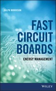
The textbook representation of a transmission line usually shows increments of series inductance and shunt capacitance. For parallel traces, a circuit representation is shown in Figure 2.1.
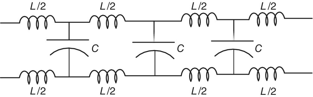
Figure 2.1 The lumped parameter model of a transmission line. L is inductance per unit length. C is capacitance per unit length.
It is convenient to use the language of circuit theory to get us started. In this network, the current that flows into the first increment of inductance charges the first increment of capacitance. As time progresses, a wave, observable as a voltage, propagates through the network storing energy in distributed capacitance and inductance at a constant rate.
The electric and magnetic field patterns around a trace over a ground plane are shown in Figure 2.2. This field pattern propagates with time along the transmission line.
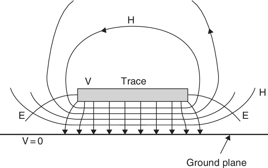
Figure 2.2 The field pattern around a trace over a ground plane (microstrip).
The voltage that is applied to the transmission line cannot be an ideal step function as this creates many philosophical problems including the need for infinite power. To avoid this issue, we assume that all voltages applied to a conductor geometry have a finite rise time. As you will see, what happens in this rise time is important and will be discussed in more detail later.
When a voltage is first connected to a transmission line, the resulting action is called a wave. This initial wave consists of a rising voltage and a rising current flow. The current is placing charge into the capacitance of the line. The voltage implies an electric field and the current flow implies a magnetic field. As the wave propagates, the current must continue to flow at a steady rate. Behind the wave front the electric and magnetic field intensities are unchanging. The magnetic field is supported by a forward and return current that must flow behind the wave front. This current crosses the transmission line at the leading edge of the wave. One way to describe this current flow is to say it is charging the capacitance of the line. Figure 2.3 shows the nature of the current as a wave moves along a transmission line.

Figure 2.3 The flow of current in a wave as it moves along a transmission line.
We are very limited in our ability to make useful displays of wave action. It is difficult enough to display what takes place at one point on a transmission line, let alone observing the action as if it were a moving train. Waves do things that trains cannot do. Wave reflect and transmit at discontinuities and trains crash. This inability to see the waves contributes to our difficulties. We try to picture each event on a time scale we can deal with. We might be able to animate voltage but what is really happening is the movement of energy. Animating energy or energy flow is not going to accomplish very much as this is really something we cannot see or measure. I will discuss this point later in the chapter. Energy flow is three dimensional and for traces it is cylindrical. Unlike water flow, the energy is confined even though the trace edges are not closed.
2.4 Characteristic Impedance
When a steady voltage V is first connected to a transmission line, current flows in the inductance of the line and charge is stored in the capacitance of the line. The charge Q in a unit of capacitance C is equal to the current I multiplied by time t. The capacitance C is thus equal to
An increment of magnetic flux in space has an inductance equal to voltage multiplied by time t. The inductance L is the ratio of flux to current or
Dividing Equation 2.2 by Equation 2.1 and taking the square root, we see that
where Z0 is called the characteristic impedance of a transmission line. It has units of real ohms. It is a measure of the first current that will flow into a transmission line. Thus initially, a transmission line behaves like a resistance where the voltage wave shape is the same as the current wave shape. It also means that if the voltage is a sine wave the initial current is also a sine wave. Even though the characteristic impedance is measured in real ohms, there is no dissipation. The energy that enters the line is stored in the electric and magnetic fields on the line.
In circuit theory, an ideal transmission line has no losses and the input impedance for sine wave voltages is a reactance. This sinusoidal measure of a transmission line assumes all transient effects have attenuated. We will discuss sine waves and transmission lines later.
Circuit theory sees transmission lines as reactances. As strange as it sounds we are going to discuss transmission lines as resistances that store energy. This points out the difference in viewpoint between circuit theory and the one we take when we transport energy (logic). It is a different world.
The characteristic impedance of a transmission line on a logic circuit board is selected to optimize the performance of integrated circuits and at the same time limit cross‐coupling. In many designs, 50 ohms is the preferred impedance level. Board manufacturers usually add traces that can be tested in the manufacturing cycle to verify that both plating and etching processes are held within expected limits.
In many designs, the trace lengths are short enough that the properties of the transmission line are not critical. The control of characteristic impedance is still important to control initial current demand, cross–coupling, and manufacturing repeatability. The control of characteristic impedance is a key factor in providing signal integrity (SI).
2.5 Waves and Wave Velocity
Waves are a common occurrence in nature. We see ocean waves and light waves and hear sound waves. We expect a flag or a tree to wave in a breeze. In many ways, we expect nature to use a wave mechanism to move or trap energy. We expect waves when potential and kinetic energy are linked together. The waves we are interested in move electrical energy back and forth in transmission lines. Within a short period of time, there may be hundreds of waves resulting from one switching event taking energy from a source. In one sense, there is only one block of energy in action but for many reasons it is practical to break up the action into waves that reflect and transmit at transition points. The rule we follow is that a wave at a transition point becomes one or two new waves and the first wave is discarded. At a 0 impedance point there is no transmission. At an open circuit there is no transmission but the arriving voltage doubles. The voltage at any point in a transmission is the sum of the wave amplitudes that pass that point. It makes no difference which direction the wave is traveling. This is why it is necessary to idealize a wave as being its transition (leading edge). A wave contributes a voltage to a point after the leading edge has passed that point. With the rules we have set up, a wave cannot pass a point more than once. We break up the action into waves that we can handle and then put the waves back together to see the end result which we can measure.
When a voltage is switched onto a transmission line, nature takes this as an opportunity to spread energy into a new volume of space. We know that energy begins to propagate as a wave along the line based on the geometry of the line. The leading edge adds charge to the line linearly with time. Using the definition of capacitance, we can relate the time it takes for the leading edge to pass one point
where w, ℓ, and h are width, length, and conductor spacing, respectively. Solving for the permittivity of free space,
Using the definition of permeability and knowing the magnetic flux increases linearly during the passage of the leading edge, we can relate time to the dimensions of the transmission line.
The product of Equations 2.5 and 2.6 shows that

On a circuit board, traces are usually spaced from a conducting plane by a dielectric called glass epoxy. This material has a relative dielectric constant εR of about 4. At a GHz the value falls to 3.5. The permittivity of a dielectric is equal to εRε0. The wave velocity in a dielectric is the speed of light reduced by the square root of the relative dielectric constant or

The field energy of a typical surface trace on a circuit board is located mainly in the dielectric under the trace. The field energy above the trace is in air. The energy in air travels faster than the energy in the dielectric. The effect is to spread out the leading edge of the wave using the transmission line.
2.6 The Balance of Field Energies
The initial energy that enters a transmission line is simply VI times time. This must be equal to the sum of electric and magnetic field energy or
The ratio of electric to magnetic energy that enters a length of transmission line is

Using Equation 2.3, it is obvious that this ratio is unity.
Thus, in every initial transmission, the moving energy is divided equally between electric and magnetic fields.
2.7 A Few Comments on Transmission Lines
The transmission lines used on a typical printed circuit board are traces over a conducting plane or traces between two conducting planes. The literature treats several other trace arrangements including side‐by‐side traces, asymmetrical traces between conducting planes, and traces between grounded trace pairs. Beside trace arrangements, transmission lines can be coaxial cables or ribbon cables. There are issues of cost and application but our concern is basically SI on circuit boards. The important factors we consider include terminations, reflections, crosstalk, energy containment and energy movement. The specific trace geometry will be mentioned only when it is relevant.
Circuit theory stresses loop or node analysis. For transmission lines, the return current path forms a loop that has little to do with circuit analysis. If the loop area relates to cross‐coupling or radiation we will be very specific. The return current path is critical because it defines the characteristic impedance of the transmission line. In our discussions, a controlled return current path is assumed even though it is not shown.
We often use single‐line diagrams showing individual waves traveling in either direction. The waves will be shown as having a leading edge that is symbolic. In practice the leading edge may spread out over the entire transmission path making an actual wave depiction somewhat impractical. Whatever the picture, if energy is in motion it will move at the speed of light in the dielectric involved. The symbolic leading edge of a wave indicates the direction of wave travel which is of course key information. The leading edge also makes it easier to see how the voltage derivative explains current flow in the capacitance of the line.
2.8 The Propagation of a Wave on a Transmission Line
To start, let us connect a voltage source to a transmission line. An initial voltage would require immediate field energy. Since this is impossible, an initial voltage must start from 0 and rise in a finite time. Since there cannot be magnetic field energy present in zero time, the current must also start from 0. In a rise time, the full voltage and full current must be present at the input terminals. In the second rise time period the wave has progressed at the speed of light and the voltage and current are at their limiting value at the input terminals. The ratio of voltage to current flow is the characteristic impedance of the line as given in Equation 2.3. Along the transmission line, where the voltage is in transition, a displacement current crosses the transmission line in the changing D field. This current path is continuous from the voltage source, along the trace, through the space between the conductors, and on the return conductor. In the third rise time period the current loop is one increment longer and a fixed voltage and current are present on the line. Stated again, the forward current crosses the line in the space of the leading edge as it moves down the line. The changing D field in this space is equal to the return current flow. This is a very important idea to grasp.1
The movement of energy in a transmission line is often paralleled with the action of a group of pendulums. When the first pendulum hits a series of suspended balls, the last pendulum receives the energy and moves. The velocity of the energy motion depends on the elastic properties of the balls. This parallels the transfer of energy in a drive shaft where mechanical stress is propagated. In this analogy, the energy flow is an impulse.
2.9 Initial Wave Action
The wave action that first propagates on the transmission line carries energy in an electric and magnetic field. As the wave propagates, energy is deposited in the capacitance and inductance of the line. This deposition occurs as the leading edge passes each point. The energy behind the wave front is carried at the speed of light in both the E and H fields although the fields are unchanging. When the wave reaches the end of the line, energy has been deposited in the line capacitance and inductance and field energy is still moving along the entire line toward the termination (load).
If the transmission line is terminated in a resistor equal to the characteristic impedance Z0, the energy in the wave flows along the line and into the resistor and all apparent wave action stops. There is field energy in motion and energy stored in the line capacitance and inductance. The resistor will dissipate energy until the voltage source is removed and all the energy in the transmission line reaches the resistor. This energy cannot be put back into the power source. This wave action is shown in Figure 2.4.
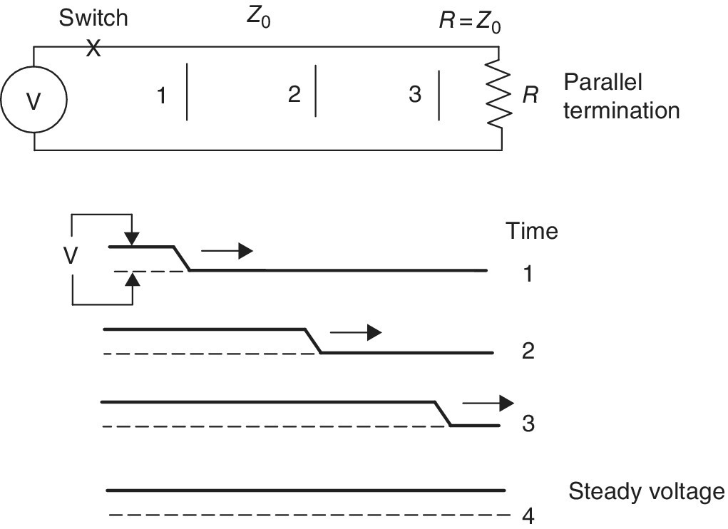
Figure 2.4 The wave action associated with a transmission line shunt terminated in its characteristic impedance.
A second representation showing wave action is given in Figure 2.5.
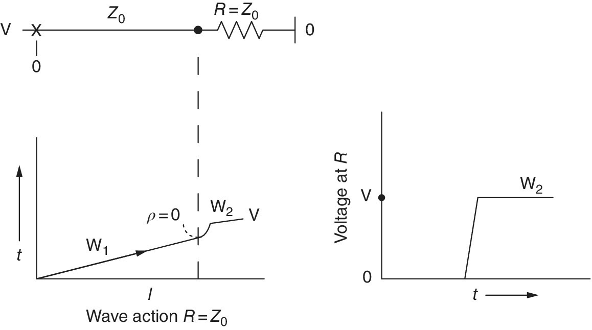
Figure 2.5 The wave action on a transmission line shunt terminated in its characteristic impedance.
In this representation, time is shown on the vertical axis and wave activity along the transmission path is shown on the horizontal axis. The U‐shaped “cups” on the diagram represent points in time and position where waves will transition. Usually a transition is a reflection back and a transmission forward. For the cup at time t = 0 and position ℓ, the closure of the switch results in a transmission W1 forward into the line. When the wave reaches the resistor R, there is no reflection. The forward transmission wave W2 is a voltage V.
In some applications, it may be desirable to terminate a line in a Zener diode in series with a terminating resistor. The Zener clamps the reflected voltage and terminates the line until wave action stops. This avoids damage to the input gate and allows the final voltage to hold without dissipating energy.
2.10 Reflections and Transmissions at Impedance Transitions
There are many places on a circuit board where the characteristic impedance of the transmission path changes. This can include sources of logic and energy, as well as at logic terminations. The wiring from an IC to pads or from pads to a capacitor are examples of short transmission lines that are often not considered. A termination can be an open circuit, a resistor, or another short transmission line. Terminations involving a general RLC network will not be considered.
On many board designs, the leading edges may transition slowly enough so that reflections do not occur. We assume zero rise times to develop equations for reflection and transmission coefficients. The criteria for when to apply these equations is given in Section 2.13.
At a transmission, the initial forward voltage is V1, the reflected voltage is VR, and the transmitted voltage is VL. Using circuit theory the relationship between these three voltages is
Assume the initial transmission line has a characteristic impedance of Z0 and the terminating transmission line or resistance is ZL. The currents must satisfy the relationship
Eliminating VL between Equations 2.13 and 2.14 and solving for the ratio VR/V1
where ρ is called the reflection coefficient.
The reflected wave has a voltage equal to
Eliminating VR between Equations 2.13 and 2.14 and solving for the ratio VL/V1,

where τ is called the transmission coefficient.
The transmitted or forward wave is equal to
The reflection coefficient ρ at an open circuit is 1. This means that the reflected wave amplitude equals the forward wave amplitude. The resulting voltage at the open circuit is double the forward wave voltage. Energy continues to flow into the transmission line doubling the voltage. If the transmission line is terminated in a short circuit then the reflection coefficient is −1. This means that the voltage of the reflected wave is reversed in polarity. Short circuits do not dissipate energy; they simply reflect the wave. If the termination is equal to Z0, then there is no reflection and the energy flows directly into the termination.
The transmission coefficient τ at an open circuit is 2. The voltage at the output terminals is double the arriving wave voltage. If the output is shorted, the transmission coefficient is 0. If the output is terminated in Z0 the transmission coefficient is 1, which means that there is no reflection and all the energy proceeds forward.
When a wave reaches the end of a transmission line terminated in a voltage V, the terminating impedance is 0 and there is no transmission. The reflection coefficient is −1 and the reflected voltage is the terminating voltage less the reflected voltage. In effect, the reflected wave returns the voltage on the line to V.
The reflection and transmission equations given above are very general and apply to any waveform. For sine waves, the voltages and loads can use the complex notation of circuit theory. See Appendix A for a review of this notation. When sine waves are involved, sums and differences are also sine waves. When other waveforms are involved this simplification is not available. The voltages on the following transmission line terminations are all step functions. Each reflected or transmitted wave is assumed to be another step function with the same rise and fall time. Each combination of waveforms is unique. This makes it more difficult to represent each method of termination. This is why it is helpful to use two different representations to display the wave action.
2.11 The Unterminated (Open) Transmission Line
The voltage representation of this wave action is shown in Figure 2.6. The rise time is assumed to be a small part of the forward transit time.

Figure 2.6 The voltage waveforms on an ideal open circuit transmission line for a step input voltage. (a) Individual waves and (b) The sum of the waves.
A second representation of this wave action is shown in Figure 2.7. Note the reflections at the voltage source and at the open circuit. At the open circuit, two new waves W2 and W3 are generated. At the voltage source there are no transmitted waves. The reflected waves are the incident waves reversed in polarity.
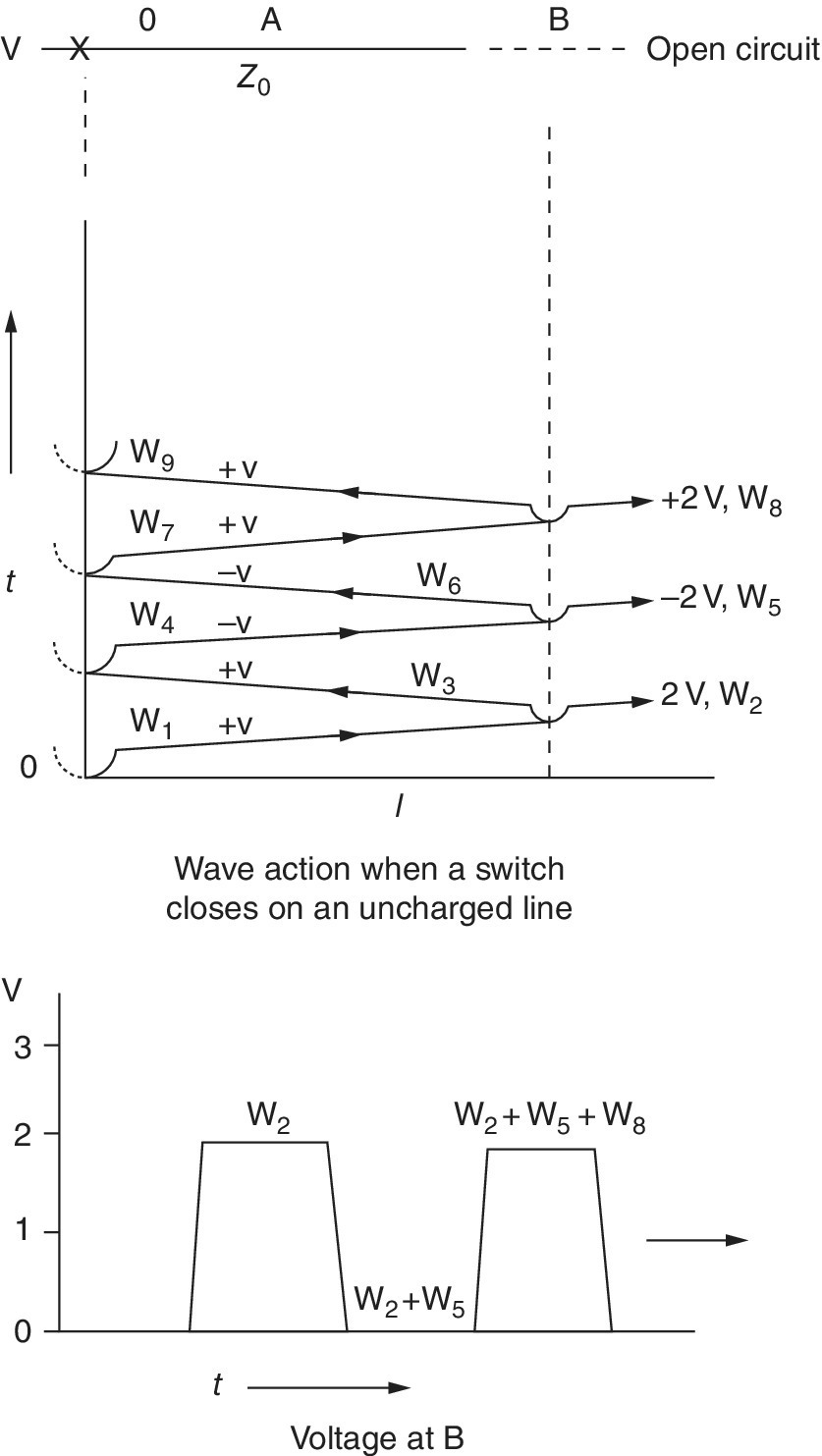
Figure 2.7 The voltage waveforms on an ideal open circuit transmission line for a step input voltage.
When the reflected wave W3 reaches the voltage source, a second reflection W4 takes place. This reflected wave W4 must have an amplitude of –W3. The current for this wave is supplied by half the charge stored in the line capacitance.2 The conversion to a negative current and a magnetic field takes place along the line at the leading edge of W4. The voltage at the source supplies no further energy to the line.
When W4 reaches the open end of the line, the negative current cannot flow in the open circuit; so, a new wave must return the output voltage to 0. The leading edge of this wave W6 converts the remaining energy in the capacitance to current and stores energy in the magnetic field of the line. The full cycle is complete when the last or sixth wave reaches the source. Without losses, this wave sequence will repeat over and over.
Four waves (W3, W4, W5, and W6) constitute one full cycle of what might be called a resonance. Two waves place electric field energy on the line. Then the next two waves convert this energy from an electric field to a magnetic field. After two round trips of waves, the next electric field energy comes from the existing stored magnetic field, not from the voltage source. This assumes no losses.
The open transmission line behaves just like the LC tank circuit of circuit theory. The difference is that step voltages are involved instead of sine waves. The lesson is simple. Without a way to lose energy, an ideal open transmission line must oscillate. Note that the voltage pattern at points A and B are different.
In the oscillating transmission line, the voltage source supplies no energy after the first round trip. The waves that are moving back and forth convert field energy back and forth between the magnetic and electric forms. In these waves, there is no net energy flow, only energy conversion. Remember, we showed that the initial wave carried exactly equal amounts of electric and magnetic field energy.
The fact that an ideal open transmission line oscillates when excited by a step wave should not be a surprise. There is inductance, capacitance, energy, and no intentional losses. In circuit theory, this is a tank circuit that supports a decaying sine wave. In this example the reflections are step functions. We know that in practice there are losses and the voltage soon stabilizes at the level of the initial wave. When the logic state is changed back from a 1 to a 0, the voltage changes but the energy stored on the capacitance of the line is not removed. This means that the line must oscillate. In circuit theory voltages just disappear from the circuit. The truth is that when energy is transported or is in transition it must eventually be dissipated and this takes time.
When the logic switch shorts the open line, the leading edge of a wave converts the energy in the line capacitance to magnetic field energy which we can sense as current flow. This current does not come through the logic switch as there is no new energy added to the line. When this wave reaches the open end of the line, the reflection converts the magnetic field energy back to electric field energy which appears as a negative voltage. What we see is wave action that appears as a square wave of voltage that goes from +V to –V. It may seem strange, but when there is voltage there is no current and when there is current there is no voltage. As before, when there is energy on a transmission line and there is no terminating resistor, the energy will transfer back and forth in a pattern we recognize as a resonance.
The presence of a negative voltage assumes the logic gate will accept this voltage without causing a diode to conduct. A conducting diode dissipates energy and this modifies the wave action. There is always the issue of whether this dissipation is within the rating of the integrated circuit. A parallel external diode would only provide protection if it conducted at a lower voltage. A germanium diode conducts at a lower voltage than silicon. It is temperature limited and may not be an acceptable protection device.
The following sections discuss various transmission line configurations. The wave action is discussed mainly in terms of voltage transitions. The function of the individual waves is not always discussed. Note that some energy is dissipated when energy is moved in and out of a magnetic field. Some energy is dissipated when it is moved into and out of a capacitance.
2.12 The Short‐Circuited Transmission Line
The pattern of voltage waves is shown in Figure 2.8a and the corresponding pattern of current waves is shown in Figure 2.8b. Unlike the open‐circuit case, there is no oscillation and the current builds up in a step manner.
Figure 2.8 The voltage pattern of waves on a short‐circuited transmission line. (a) Individual waves and (b) The sum of the waves.
The initial voltage wave stores energy in both the line capacitance and inductance. The first reflected wave converts electric field energy to magnetic field energy. This results in doubling the current flow behind the wave front. When this wave returns to the source, the voltage source must support three units of forward current: the initial current, the converted current, and the current for the next forward wave. After the next round trip of wave action, the current increases to 5 units. The arrows in the figures indicate the wave direction and not the current direction which always points toward the short on the transmission line. This is another example of where the current flow direction and the wave directions are not the same.
A second representation of wave action for a shorted transmission line is shown in Figure 2.9.
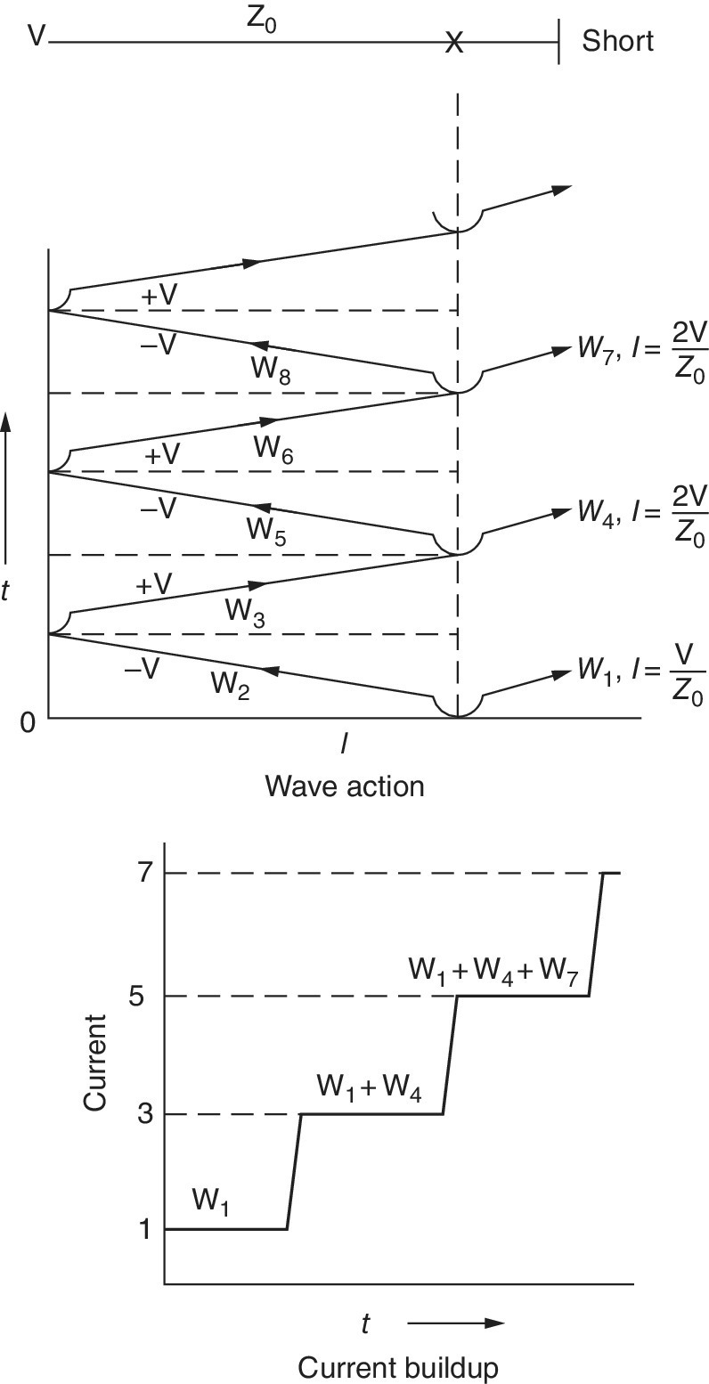
Figure 2.9 The staircase current pattern for a shorted transmission line.
2.13 Voltage Doubling and Rise Time
In Section 2.10, we saw that there is voltage doubling on an open transmission line. This occurred because we assumed zero rise time for the initial step voltage. With a finite rise time, a doubling of voltage can only occur if the line is longer than 2.5 times the distance traveled by the wave in the rise time. In many circuit board applications, line terminations are not required. Because clock rates are increasing, this problem needs to be addressed as each design is considered.
At 1 GHz, a wave travels about 15 cm in one clock cycle. The distance traveled in a rise time is about 1.5 cm. Voltage doubling will begin to appear if the line is longer than 3.7 cm. Since there can be about 1.5 cm of line inside a component, the maximum trace length before voltage doubling occurs is about 0.7 cm. It is safe to say that termination resistors are needed above 1 GHz. If the forward wave is at half voltage, the reflection will double the voltage and no termination resistors are needed (see Section 2.16).
This doubling action is shown in Figure 2.10 where the line length is given in terms of the distance traveled by the wave. This figure can easily be scaled by increasing the line length and using this same factor on all of the rise times.
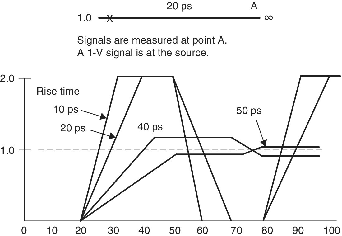
Figure 2.10 Rise times and the reflections from an unterminated transmission line.
2.14 Matched Shunt Terminated Transmission Lines
In Figure 2.11 an ideal voltage source V is connected to a length of 50‐ohm transmission line terminated in a matched (shunt) 50‐ohm resistor. When the switch X connects the transmission line to the resistor, the voltage at the switch drops to 2.5 V and a wave of −2.5 V travels back toward the source. At the source, this wave reflects and a wave of +2.5 V travels forward. At the load this voltage adds to the initial voltage making the total voltage 5 V. There is no reflection as the line impedance matches the termination resistor and all wave action stops.
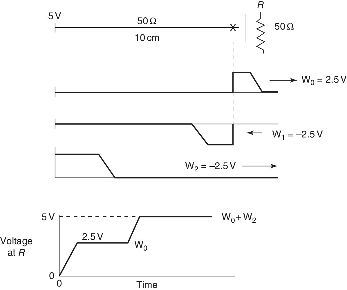
Figure 2.11 Matching shunt termination using a remote switch.
This wave action occurs any time a circuit makes a request for energy from a remote point. The intervening transmission line determines the level of initial current and the time it takes for the request to be met. The voltage source could be a decoupling capacitor.
This method of line termination dissipates energy as long as the logic switch is closed. It is used on long lines where voltage doubling is a problem. When the switch is opened, a wave must travel toward the voltage source that sets the current to 0. In an ideal line the energy in motion before the switch opens cannot be lost. In this case, the arriving energy is stored in the line capacitance. This means that the return wave doubles the voltage across the open switch which can destroy the switch. If the logic is to be disconnected from the transmission line it should be done on the other side of any termination. This avoids any voltage doubling. Once the switch opens, the line has inductance, capacitance, and energy and there is no terminating resistor. The result is an oscillation on a resonant transmission line.
A second method of displaying wave action on this transmission line termination is shown in Figure 2.12.

Figure 2.12 A matching termination using a remote switch.
When the switch closes, a wave W1 of amplitude V/2 enters the resistor. Wave W2 moves toward the voltage source and reflects. There is no wave transmission into a voltage source. The reflected wave W3 reverses the polarity of W2. When W3 reaches the resistor R there is no reflection as the resistor matches the characteristic impedance of the line. The transmission coefficient is unity and the wave W4 = W3 enters the resistor. Two waves of amplitude V/2 have arrived at the resistor R making the final voltage equal to V.
If the transmission line characteristic impedance is higher than the load, then the reflected waves will be smaller and more wave action is required to bring energy to the load. This is shown in Figure 2.13.

Figure 2.13 The voltage at a termination when there is a mismatch in impedances.
If the resistor R is 25 ohms in Figure 2.11, then the wave into this resistor would be 0.666 V and the reflected wave would be −0.333 V. The current for this wave comes from the charge stored in the line capacitance. At the source, the reflection reverses the wave polarity and a wave of +0.333 V moves forward. At the load, another reflection and transmission takes place. The voltage at the load increases in the steps 0.666 V, 0.888 V, 0.962 V, 0.986 V, and so on. In most practical situations, it is not possible to see these step voltages. What is seen is a smooth leading edge that appears exponential in character. Remember that wave character involving transmission lines is not the same as transient behavior described by linear circuit theory. In circuit theory, this exponential rise in voltage would be explained by assuming a parasitic series inductance or a parasitic shunt capacitance. In this example, the time it takes for the voltage to reach its final value involves the path length as well as the capacitance, the dielectric constant, and the inductance in the transmission path. Assuming the delay is the result of inductance alone is incorrect. It is the result of moving energy which is a very different picture. This wave action is shown in Figure 2.14.
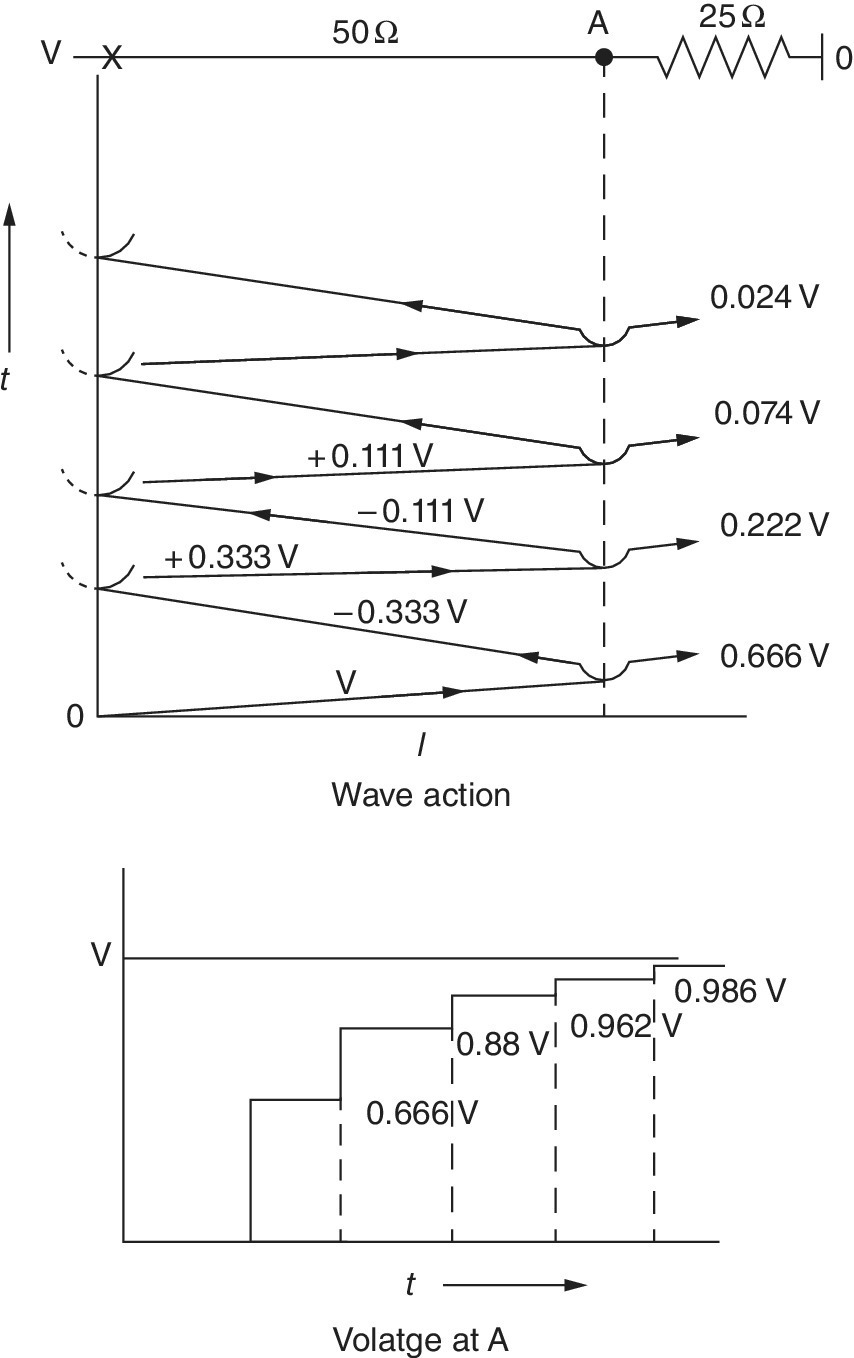
Figure 2.14 The voltage at a termination when there is a mismatch in terminating impedance.
2.15 Matched Series Terminated Transmission Lines
In Figure 2.15 an ideal voltage source is connected to a series switch, a line matching series resistor of 50 ohms, and a length of 50‐ohm line that is unterminated. When the switch connects a voltage to the line, a wave of amplitude V/2 travels down the line. At the open end of the line the voltage doubles to V. The reflected wave converts the magnetic field energy to electric field energy. When this wave reaches the matching resistor at the source, the voltage across the resistor is 0 and all wave action stops. This is an ideal transmission line configuration for short rise time logic. The matching series resistor must be located very close to the voltage source and the logic switch for this wave action to take place. If the integrated circuit is built with an internal series line‐matching resistor, then no external series matching resistor is needed. When the switch returns the logic voltage to 0, the forward wave is –V/2. At the open circuit the wave voltage is doubled and the resulting voltage at the open circuit is 0 V.
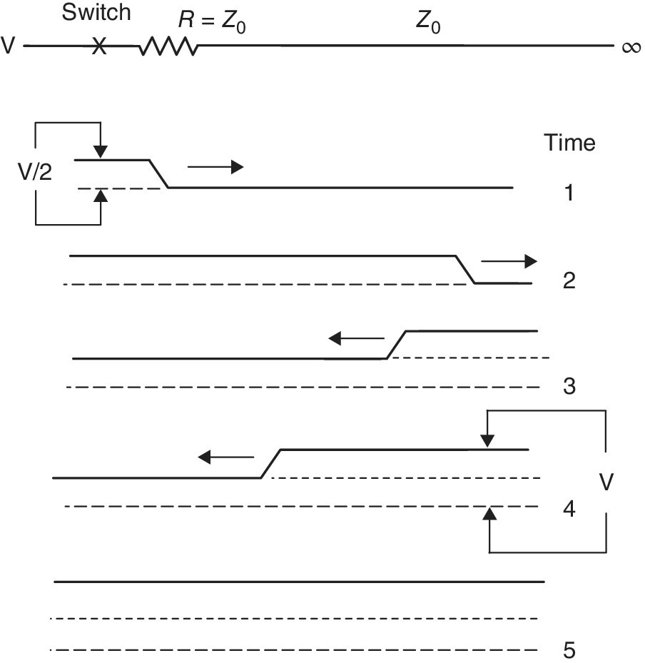
Figure 2.15 A series (source) terminated transmission line.
2.16 Extending a Transmission Line
Logic operations can involve extending transmission lines from a source of energy such as a decoupling capacitor through a switch to a remote gate G. In Section 3.2, we will discuss the fact that there are several sources of immediate energy in the IC. Assume for the moment that these energy sources are not present. The transmission line to the left of a switch is labeled d1. The line to the right is labeled d2 and stores no energy. This transmission line arrangement is shown in Figure 2.16. Initially the switch is open.
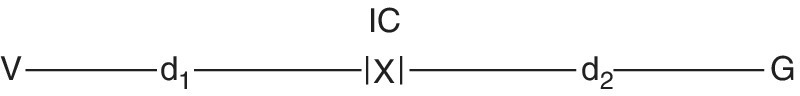
Figure 2.16 A typical transmission line.
At the moment where d1 connects to d2, waves must propagate on each transmission line. The connected voltage drops to V1. The voltage of the wave going left is –(V–V1). The voltage of the wave going right is V1. The energy in d1 in a distance s must travel a distance 2s to get to the point s on d2. The initial energy in a distance s is ½CV2. The energy in motion is half magnetic. Therefore, in a distance 2s, the energy in the electric field is ¼CV2. This equation shows that V1 = V/2. This means that there is a wave growing in length traveling in both directions moving energy from d1 to d2. The wave moving left is depleting energy in d1 and this energy is moving right into d2. If the relative dielectric constant is 4, the wave velocities are c/2. A full understanding of what occurs requires a relativistic treatment.
The energy flowing into d2 comes from d1. Since the wave in d1 is traveling left and the energy in d2 moving right, the rise time for the forward wave in d2 is doubled over the rise time in the initial switching action. This doubling of rise time does not usually occur as there is usually enough local energy in parasitic capacitance to fill in the gap. The wave that travels right into d2 carries energy forward. This energy flow as required is half electric and half magnetic. When the wave front traveling left reaches the voltage source, the wave reflects and a positive wave moves forward. This wave converts the magnetic field energy moving left into electric field energy that is stationary (stored in the line capacitance.) This wave action returns the energy to d1. Remember that the combined stationary E and H field along the line implies energy flow.
When the wave moving forward in d2 reaches the open end of the line, the wave reflects. The wave front converts arriving magnetic energy into electric field energy doubling the voltage on the line. This wave action places energy in the line capacitance of d2. When this wave reaches the forward wave, all wave activity stops as the currents are 0 and the voltages are equal. Wave action has moved a block of energy from d1 to d2 and supplied a block of energy to d1.
At first glance this seems like a perfect solution where no terminating resistor is needed. In practice, several logic elements can make a demand for energy at the same time. If these demands are made on one transmission line to an energy source the wave action does not stop as described above. A separate power trace for each logic line is impractical. The only viable solution is to provide an energy source in or at the IC. In this situation, the full voltage moves forward and voltage doubling can do damage. This is the reason why a series matching resistor is needed.
2.17 Skin Effect
A full treatment of skin effect on circuit traces is complex. An approximate picture of this effect can be helpful.
The textbook approach to skin effect assumes a plane electromagnetic field reflecting from an infinite conducting plane. The field is sinusoidal so that the surface currents that flow are also sinusoidal. The field intensity at any depth is a function of frequency, conductivity, and permeability. For copper the relative permeability is unity. A skin depth at a given frequency is the depth where the field intensity is reduced by a factor of 1/e or 36.8%. The frequency that is used when logic is involved is obviously a compromise. The frequency that is often used is 1/πτR where τR is the rise time of the logic.
The attenuation factor for an infinite conducting plane and a plane sinusoidal wave is
where h is the depth and
The permeability μ0 of space is 4π × 10−7 T m/A. The conductivity of copper is σ = 0.580 × 10⁸ A/V m and f is frequency.
When h = 1/α the field intensity is reduced by a factor of 36.8%. This is called one skin depth. For copper at 1 MHz, the skin depth is 0.65 µm. At 100 MHz, the depth is 0.065 µm. This approximation is a reminder of just how little of the copper gets used in a single transmission. If the copper is plated this is where the initial current flows.
It is interesting to point out that a static voltage without current flow along a transmission line requires a surface charge. These charges are the first to move when wave action takes place. Just a reminder, electron velocity in a transmission line is only centimeters per second.
Problem Set
- 1 If the dielectric constant increases by 2%, what is the change in characteristic impedance?
- 2 A transmission line is 10 cm long. The dielectric constant is 4 at 10 MHz and 3.5 at 1 GHz. What is the arrival time difference for sine waves?
- 3 Show that 1 − τ = ρ
- 4 A 5‐V wave on a 50‐ohm line terminates on a 60‐ohm line. What is the voltage of the transmitted wave? What is the reflected voltage?
- 5 A 50‐ohm line terminates in two 50‐ohm lines. What are the reflected and transmitted voltages if the initial voltage is 5 V?
- 6 What is the field intensity at two skin depths?
- 7 An unterminated transmission line is oscillating. The dielectric constant is 3.5. What is the frequency if the length of the line is 5 cm?
- 8 A request for energy is made over a 50‐ohm line that is 4 cm long. The dielectric constant is 3.5. The logic is 5 cm away. Assume two round trips are needed. What is the delay?
Glossary
- Characteristic impedance
- The ratio of initial voltage to initial current on a transmission line. On an ideal line the ratio is constant until a reflected wave returns to the source (Section 2.4).
- Conductivity
- A measure of a material to conduct current. It is the reciprocal of resistivity. The resistance of a conductor is R = ρl/A where ρ is resistivity, l is the length of the conductor, and A is the cross‐sectional area (Section 2.17).
- Exponential
- Growth or decay of physical phenomena where the activity is proportional to the amount present involves a natural constant e which is 2.718. The voltage on a capacitor discharged by a resistor is said to be exponential decay (Section 2.14).
- Flux
- Usually a representation of the magnetic B field. Line density indicates field intensity.
- Free space
- Ideally a vacuum removed from conductors or charges. Practically, the space around a circuit not near conductors.
- Ground plane
- A conducting surface usually larger than any associated components. On a circuit board, it can be a conducting layer (Section 2.3).
- Leading edge
- The voltage pattern at the front of a wave.
- Line
- A transmission line. A trace running parallel to a conductor.
- Lumped parameter
- A circuit representation of a conductor geometry where distributed parameters are represented by series and parallel elements. On a transmission line, every increment of the line has inductance and capacitance. The lumped parameter model is a series of inductors interspersed with shunt capacitors (Section 2.3).
- Matching termination
- Usually a resistor equal to the characteristic impedance of a transmission line. A terminating transmission line with a matching characteristic impedance.
- Reflection coefficient
- The ratio of a reflected wave amplitude to a forward wave amplitude at a transmission line termination. For a transmission line this ratio can cover the range −1 to +1. At a short circuit the reflection coefficient is −1. For an open circuit the reflection coefficient is +1. This means the voltage is doubled (Section 2.10).
- Relative permittivity
- The dielectric constant.
- Resonance
- A condition where energy is in constant transition between two storage mechanisms. On a transmission line the energy transfers back and forth between electric and magnetic fields. On a pendulum, energy transfers back and forth between energy of motion and energy of position (Section 1.11).
- Rise time
- The length of time it takes a wave to transition from 10 to 90% of final value. It is usually a voltage measure. Other definitions are frequently used.
- Series termination
- A termination, usually a resistor, that is in series with the source voltage on a transmission line.
- Shunt termination
- A termination that is placed across a transmission line usually at the end of the line.
- Skin depth
- A measure of how far into a conductor surface currents penetrate. One skin depth implies the current falls to 1/e or 36.8% of the surface value.
- Skin effect
- A phenomena that occurs in conductors where changing currents tend to flow on the surface of conductors. The measure is made for sine waves but applies to any waveform (Section 2.17).
- Step voltage
- A voltage that changes value in zero time. This is of course impossible as the energy stored in parasitic capacitance would have to appear in zero time and this would require infinite power. In practice a step voltage has a finite rise time (Section 2.11).
- Termination
- The impedance at the ends of a transmission line. A termination can be an open circuit, a short circuit, or a resistor.
- Transmission coefficient
- The ratio between a transmitted wave and an arriving wave at a transmission line termination. The coefficient can cover the range 0–2. At a short circuit, the coefficient is 0. At an open circuit, the coefficient is 2, which means the voltage is doubled (Section 2.10).
- Transmission line
- A conductor geometry that supports the flow of electromagnetic energy.
- Unterminated line
- A transmission line terminated at an open circuit. The actual termination is a small capacitance that can modify the leading edge of an arriving wave.
- Wave
- A transition in voltage that travels along a transmission line usually characterized by a leading edge followed by a steady voltage. A wave can carry, deposit, or transform energy. The term wave is also used for sinusoidal transmissions where there is no leading edge. Waves can be confined by conductors or they can move in free space. There are wave patterns that appear stationary. A steady pattern moving in or on a media can also be called a wave.
Answers to Problems
- 1 The capacitance increases by 2% and the characteristic impedance drops by 1.414%.
- 2 42 ps.
- 4 τ = 1.091, ρ = 0.091.
- 5 Both the reflected and transmitted waves are 3.333 V.
- 6 One skin depth is 36.8%. The square of this percentage is 13.5%.
- 7 802 MHz or four different wave patterns.
- 8 The distance travelled is 27 cm at a velocity of 160 m/µs. The time is 1.7 ns.