
10
SOFT-SWITCHING IN DC-DC CONVERTERS AND HALF-BRIDGE RESONANT CONVERTERS
10.1 INTRODUCTION
In converters so far, we have discussed hard-switching in the switching power-pole, as described in Chapter 2. In this chapter, we will look at the problems associated with hard-switching and some of the practical circuits where this problem can be minimized with soft-switching.
10.2 HARD-SWITCHING IN SWITCHING POWER POLES
Figure 10.1a shows the switching power-pole, and Figure 10.1b shows the hard-switching waveforms, which were discussed in Chapter 2. Because of the simultaneous high voltage and high current associated with the transistor during the switching transition, the switching power losses in the transistor increase linearly proportional to the switching frequency and the sum of the times ![]() and
and ![]() , shown in Figure 10.1b, assuming an ideal diode,
, shown in Figure 10.1b, assuming an ideal diode,

FIGURE 10.1 Hard switching in a power pole.
In hard-switching converters, in addition to the switching power losses decreasing the energy efficiency, the other problems are device stresses, thermal management of power losses, and electromagnetic interference resulting from high di/dt and dv/dt due to fast transitions in the converter voltages and currents. The above problems are exacerbated by the stray capacitances and leakage inductances associated with the converter layout and the components.
In order to reduce the overall converter size while maintaining high energy efficiency, the trend is to design DC-DC converters operating at as high a switching frequency as possible (typically 100–200 kHz in small power ratings), using fast-switching MOSFETs. At high switching frequency, the switching power losses become unacceptable if hard-switching is used, and hence soft-switching is often employed, as briefly described in this chapter.
The problems described above associated with hard-switching can be minimized by means of the following:
- Circuit layout to reduce stray capacitances and inductances.
- Snubbers to reduce di/dt and dv/dt.
- Gate-drive control to reduce di/dt and dv/dt.
- Soft-switching.
It is always recommended to have a layout to reduce stray capacitances and inductances. Snubbers consist of passive elements (R, C, and possibly a diode) to reduce di/dt and dv/dt during the switching transient, by shaping the switching trajectory. The trend in modern power electronics is to use snubbers only in transformer-isolated DC-DC converters, where the leakage inductance associated with the high-frequency transformer can be substantial, in spite of a good circuit layout. Generally, snubbers do not reduce the overall losses; rather, they shift some of the switching losses in the transistor to the snubber resistor. A detailed discussion of snubbers is beyond the scope of this book; the interested reader is advised to refer to [1].
By controlling the gate voltage of MOSFETs and IGBTs, it is possible to slow down the turn-on and turn-off speed, thereby resulting in reduced di/dt and dv/dt, at the expense of higher switching losses in the transistor. The above techniques, at best, result in a partial solution to the problems of hard-switching.
However, there are certain topologies and control, as described in the next section, that allow soft-switching that essentially eliminates the drawbacks of hard-switching without creating new problems.
10.3 SOFT-SWITCHING IN SWITCHING POWER-POLES
There are many such circuits and control techniques proposed in the literature, most of which may make the problem of EMI and the overall losses worse due to large conduction losses in the switches and other passive components. Avoiding these topologies, only a few soft-switching circuits are practical.
The goal in soft-switching is that the switching transition in the power pole occurs under very favorable conditions, that is, the switching transistor has a zero voltage and/or zero current associated with it. Based on these conditions, the soft-switching circuits can be classified as follows:
- ZVS (zero-voltage switching), and
- ZCS (zero-current switching)
We will consider only the converter circuits using MOSFETs, which result in ZVS (zero-voltage switching). The reason is that, based on Equation 10.1, soft-switching is of interest at high switching frequencies where MOSFETs are used. In MOSFETs operating at high switching frequencies, a significant reduction of switching loss is achieved by not dissipating the charge associated with the junction capacitance inside the MOSFET each time it turns on. This implies that for meaningful soft-switching, the MOSFETs should be turned on under a zero-voltage switching (ZVS) condition. As we will see shortly, the turn-off also occurs at ZVS.
10.3.1 Zero-Voltage Switching (ZVS)
To illustrate the ZVS principle, the intrinsic anti-parallel diode of the MOSFET is shown as being distinct in Figures 10.2a and 10.2b, where a capacitor is used in parallel. This MOSFET is connected in a circuit such that before applying the gate voltage to turn the MOSFET on, the switch voltage is brought to zero, and the anti-parallel diode is conducting, as shown in Figure 10.2a. This results in an ideal lossless turn-on at ZVS. At turn-off, as shown in Figure 10.2b, the capacitor across the switch results in an essentially ZVS turn-off where the current through the MOSFET channel is removed while the voltage across the device remains small (essentially zero) due to the parallel capacitor. This ZVS principle is illustrated by modifying the synchronous-rectified buck DC-DC converter, as discussed below.

FIGURE 10.2 ZVS in a MOSFET.
10.3.2 Synchronous Buck Converter with ZVS
As discussed in section 3.10 (Chapter 3), synchronous-rectified buck DC-DC converters are used in applications where the output voltage is very low. Figure 10.3a shows a synchronous-rectified DC-DC converter where the diode has been replaced by another MOSFET, and the two MOSFETs are provided complementary gate signals ![]() and
and ![]() . The waveforms associated with this synchronous buck converter are shown in Figure 10.3b, where the inductor is large such that the inductor-current ripple is small (shown by the solid curve in Figure 10.3b), and the inductor current remains positive in the direction shown in Figure 10.3a in the continuous conduction mode.
. The waveforms associated with this synchronous buck converter are shown in Figure 10.3b, where the inductor is large such that the inductor-current ripple is small (shown by the solid curve in Figure 10.3b), and the inductor current remains positive in the direction shown in Figure 10.3a in the continuous conduction mode.

FIGURE 10.3 Synchronous-rectified buck converter.
To achieve ZVS, the circuit of Figure 10.3a is modified, as shown in Figure 10.4a, by showing the internal diode of the MOSFET explicitly and adding small external capacitances (in addition to the junction capacitances inherent in MOSFETs). The inductance value in this circuit is chosen to be much smaller such that the inductor current has a waveform shown dotted in Figure 10.3b with a large ripple and such that the current ![]() is both positive and negative during every switching cycle.
is both positive and negative during every switching cycle.

FIGURE 10.4 Synchronous-rectified buck converter with ZVS.
We will consider the transition at time ![]() labeled in Figure 10.3b and Figure 10.4b, when the inductor current is at its peak
labeled in Figure 10.3b and Figure 10.4b, when the inductor current is at its peak ![]() in Figure 10.4a. The gate signal
in Figure 10.4a. The gate signal ![]() of the transistor
of the transistor ![]() , which is initially conducting
, which is initially conducting ![]() , goes to zero, while
, goes to zero, while ![]() remains zero, as shown in Figure 10.4b. The transition time during which the current transfers from
remains zero, as shown in Figure 10.4b. The transition time during which the current transfers from ![]() to
to ![]() is very short, and it is reasonable to assume for discussion purposes that the inductor current remains constant at
is very short, and it is reasonable to assume for discussion purposes that the inductor current remains constant at ![]() , as shown in Figure 10.5a.
, as shown in Figure 10.5a.
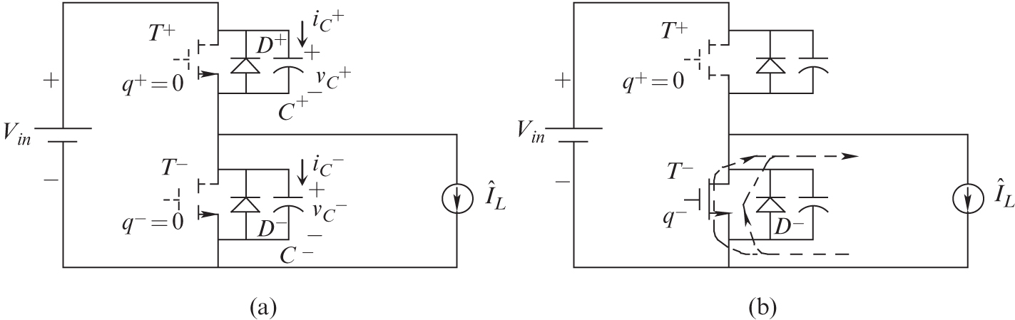
FIGURE 10.5 Transition in synchronous-rectified buck converter with ZVS.
In the circuit of Figure 10.5a with both ![]() and
and ![]() equal to zero, initially
equal to zero, initially ![]() and
and ![]() , where from Kirchhoff’s law, these two voltages must add to the input voltage,
, where from Kirchhoff’s law, these two voltages must add to the input voltage,
As the current through ![]() declines, equal and opposite currents flow through the two capacitors in Figure 10.5a, which can be derived from Equation 10.2 as follows, assuming equal capacitances
declines, equal and opposite currents flow through the two capacitors in Figure 10.5a, which can be derived from Equation 10.2 as follows, assuming equal capacitances ![]() : differentiating both sides of Equation 10.2 and multiplying both sides by
: differentiating both sides of Equation 10.2 and multiplying both sides by ![]() ,
,
As the current through ![]() declines, a positive
declines, a positive ![]() causes
causes ![]() to rise from
to rise from ![]() , and a negative
, and a negative ![]() causes
causes ![]() to decline from its initial value of
to decline from its initial value of ![]() . If this voltage transition happens slowly compared to the current fall time of the MOSFET
. If this voltage transition happens slowly compared to the current fall time of the MOSFET ![]() , then the turn-off of
, then the turn-off of ![]() is achieved at essentially zero voltage (ZVS). After the current through
is achieved at essentially zero voltage (ZVS). After the current through ![]() has gone to zero, applying Kirchhoff’s current law in Figure 10.5a and using Equation 10.4 results in
has gone to zero, applying Kirchhoff’s current law in Figure 10.5a and using Equation 10.4 results in
In Figure 10.5a, during the turn-off transition of ![]() ,
, ![]() rises to
rises to ![]() , and
, and ![]() declines to
declines to ![]() . The voltage
. The voltage ![]() cannot become negative because of the diode
cannot become negative because of the diode ![]() (assuming an ideal diode with zero forward voltage drop), which begins to conduct the entire
(assuming an ideal diode with zero forward voltage drop), which begins to conduct the entire ![]() in Figure 10.5b, marking the ZVS turn-off of
in Figure 10.5b, marking the ZVS turn-off of ![]() .
.
Once ![]() begins to conduct, the voltage is zero across
begins to conduct, the voltage is zero across ![]() , which is applied a gate signal
, which is applied a gate signal ![]() to turn on, as shown in Figure 10.4b, thus resulting in the ZVS turn-on of
to turn on, as shown in Figure 10.4b, thus resulting in the ZVS turn-on of ![]() . Subsequently, the entire inductor current begins to flow through the channel of
. Subsequently, the entire inductor current begins to flow through the channel of ![]() in Figure 10.5b. The important item to note here is that the gate signal to
in Figure 10.5b. The important item to note here is that the gate signal to ![]() is appropriately delayed by an interval
is appropriately delayed by an interval ![]() , shown in Figure 10.4b, making sure that
, shown in Figure 10.4b, making sure that ![]() is applied after
is applied after ![]() begins to conduct.
begins to conduct.
The next half-cycle in this converter is similar to the ZVS turn-off of ![]() , followed by the ZVS turn-on of
, followed by the ZVS turn-on of ![]() , facilitated by the negative peak of the inductor current.
, facilitated by the negative peak of the inductor current.
Although this buck converter results in ZVS turn-on and turn-off of both transistors, the inductor current has a large ripple, which will also make the size of the filter capacitor large since it has to carry the inductor current ripple. In order to make this circuit practical, the overall ripple that the output capacitor has to carry can be made much smaller (similar ripple reduction occurs in the current drawn from the input source) by an interleaving of two or more such converters, as discussed in section 3.11 (Chapter 3). Another advantage of this converter is its ability to respond rapidly to load change.
10.3.3 Phase-Shift Modulated (PSM) DC-DC Converters
Another practical soft-switching technology is the phase-shift modulated (PSM) DC-DC converter, shown in Figure 10.6a. It is a variation of the PWM DC-DC converters discussed in Chapter 8.

FIGURE 10.6 Phase-shift modulated (PSM) DC-DC converter.
The switches in each power pole of the PSM converter operate at nearly 50% duty ratio, and the regulation of the output voltage is provided by shifting the output of one switching power-pole with respect to the other, as shown in Figure 10.6b, to control the zero-voltage intervals in the transformer primary voltage ![]() .
.
To provide the ZVS turn-on and turn-off of switches, a capacitor is placed across each switch. This topology makes use of the transformer leakage inductance and the magnetizing current.
10.4 HALF-BRIDGE RESONANT CONVERTER
It is possible to achieve soft-switching in converters for induction heating and compact fluorescent lamps by using a half-bridge converter with soft-switching, as shown in Figure 10.7.

FIGURE 10.7 Half-bridge resonant converter.
This converter consists of two DC capacitors that establish the midpoint such that each capacitor has ![]() across them. The load in this generic circuit is represented by a resistance R in series with the resonant circuit elements
across them. The load in this generic circuit is represented by a resistance R in series with the resonant circuit elements ![]() and
and ![]() , which have a resonant frequency
, which have a resonant frequency
The switching frequency ![]() is selected to be greater than the resonant frequency:
is selected to be greater than the resonant frequency:
In Figure 10.7, two switches are switched with essentially 50% duty ratio. This results in ![]() that has a square waveform, as shown in Figure 10.8. Because the switching frequency in the resonant circuit is higher than the resonant frequency, this circuit appears inductive at the switching frequency. Therefore, the current i lags behind the voltage waveform, as shown in Figure 10.8. Since the impedance of the resonant circuit will be much higher at the harmonic frequency of the input voltage, the current will essentially have a sinusoidal waveform, as shown in Figure 10.8.
that has a square waveform, as shown in Figure 10.8. Because the switching frequency in the resonant circuit is higher than the resonant frequency, this circuit appears inductive at the switching frequency. Therefore, the current i lags behind the voltage waveform, as shown in Figure 10.8. Since the impedance of the resonant circuit will be much higher at the harmonic frequency of the input voltage, the current will essentially have a sinusoidal waveform, as shown in Figure 10.8.

FIGURE 10.8 Converter output waveforms.
At t = 0, ![]() is forced to turn off, essentially at ZVS due to lossless capacitors, and after a brief period during which capacitor voltages change, the current begins to flow through
is forced to turn off, essentially at ZVS due to lossless capacitors, and after a brief period during which capacitor voltages change, the current begins to flow through ![]() . As soon as
. As soon as ![]() begins to conduct,
begins to conduct, ![]() is gated on, and the current can flow through it when it becomes positive. At
is gated on, and the current can flow through it when it becomes positive. At ![]() ,
, ![]() is forced to turn off at essentially ZVS, and the next half-cycle ensues.
is forced to turn off at essentially ZVS, and the next half-cycle ensues.
A detailed description of such resonant circuits is provided in [1, 2].
REFERENCES
- 1. N. Mohan, T.M. Undeland, and W.P. Robbins, Power Electronics: Converters, Applications and Design, 3rd Edition (New York: John Wiley & Sons, 2003).
- 2. N. Mohan, W. Robins, T. Undeland, and S. Raju, Power Electronics for Grid-Integration of Renewables: Analysis, Simulations and Hardware Lab (New York: John Wiley & Sons, 2023).
PROBLEMS
- 10.1 In a synchronous-rectified buck converter with ZVS, shown in Figure 10.4a,
 ,
,  ,
,  , and the maximum load is
  . Calculate the filter inductance such that the negative peak current through the inductor is at least 1.5 amps.
 - 10.2 In Problem 10.1, calculate the capacitances across the MOSFETs if the charge/discharge time is to be no more than
 .
.
SIMULATION PROBLEMS
- 10.3 In a synchronous buck converter, such as that shown in Figure 10.4a,

 the filter-inductor
  and the output capacitance
  and the switching frequency
 The gate voltages are as shown below:
- Obtain the waveforms for
 and
and 
- Obtain the voltage across and the current through one of the switches. Comment on the zero-voltage/current switchings.
- Around the blanking time, obtain the currents through one of the switches and through its associated diode and the snubber capacitors.
- Obtain the waveforms for
- 10.4 In a resonant converter, shown in Figure 10.7,
 ,
,  ,
,  and
and  . The snubber capacitors across the MOSFETs are
  each. The switching frequency
  .
.- Obtain the waveforms for
 and
and  .
. - By Fourier analysis, obtain and plot
 and
and  waveforms, where the subscript 1 refers to the fundamental frequency component. Why does the current lag the voltage?
 - Plot the voltage across the capacitor and the current through it.
- Obtain the waveforms for