
3
SWITCH-MODE DC-DC CONVERTERS: SWITCHING ANALYSIS, TOPOLOGY SELECTION, AND DESIGN
In Chapter 1, we discussed various applications of power electronics, including those for energy sustainability. Some of these applications, such as harnessing solar energy using photovoltaics, use of fuel cells, and energy storage in batteries, require DC-DC converters to convert voltages and currents from one DC level to another and to operate these systems optimally. In addition to these direct applications, DC-DC converters form the basic block of conversion between AC and DC voltages, required in applications such as harnessing wind energy and efficiently adjusting the speed of drives in transportation and compressor systems for increasing energy efficiency.
3.1 DC-DC CONVERTERS[1]
Figure 3.1a shows buck, boost, and buck-boost DC-DC converters by a block diagram and how the pulse-width modulation process regulates their output voltage. The design of the feedback controller is the subject of the next chapter. The power flow through these converters is in only one direction. Thus, their voltages and currents remain unipolar and unidirectional, as shown in Figure 3.1b. Based on these converters, several transformer-isolated DC-DC converter topologies, which are used in all types of electronics equipment, are discussed in Chapter 8.
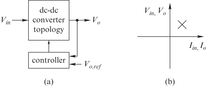
FIGURE 3.1 Regulated switch-mode DC power supplies
3.2 SWITCHING POWER-POLE IN DC STEADY STATE
All the converters that we will discuss consist of a switching power-pole that was introduced in Chapter 1 and is redrawn in Figure 3.2a. In these converter circuits in DC steady state, the input voltage and the output load are assumed constant. The switching power-pole operates with a transistor switching function ![]() , whose waveform repeats, unchanged from one cycle to the next, and the corresponding switch duty ratio remains constant at its steady-state DC value
, whose waveform repeats, unchanged from one cycle to the next, and the corresponding switch duty ratio remains constant at its steady-state DC value ![]() . Therefore, all waveforms associated with the power pole repeat with the switching time period
. Therefore, all waveforms associated with the power pole repeat with the switching time period ![]() in the DC steady state, where the basic principles described below are extremely useful for analysis purposes.
in the DC steady state, where the basic principles described below are extremely useful for analysis purposes.

FIGURE 3.2 Switching power-pole as the building block of DC-DC converters.
First, let us consider the voltage and current of the inductor associated with the power pole. The inductor current depends on the pulsating voltage waveform, as shown in Figure 3.2b. The inductor voltage and current are related by the conventional differential equation, which can be expressed in the integral form as follows:
where ![]() is a variable of integration representing time. For simplicity, we will consider the first time period starting with
is a variable of integration representing time. For simplicity, we will consider the first time period starting with ![]() in Figure 3.2b. Using the integral form in Equation (3.1), the inductor current at a time
in Figure 3.2b. Using the integral form in Equation (3.1), the inductor current at a time ![]() can be expressed in terms of its initial value
can be expressed in terms of its initial value ![]() as:
as:
 (3.2)
(3.2)
In the DC steady state, the waveforms of all circuit variables must repeat with the switching frequency time period ![]() , resulting in the following conclusions from Equation (3.2):
, resulting in the following conclusions from Equation (3.2):
- The inductor current waveforms repeat with
 , and therefore in Equation (3.2)
 (3.3)
(3.3)
- Integrating over one switching time period
 in Equation (3.2) and using Equation (3.3) show that the inductor voltage integral over
  is zero. This leads to the conclusion that the average inductor voltage, averaged over
  , is zero:
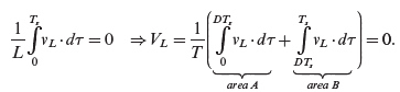 (3.4)
(3.4)
In Figure 3.2a, the area A in volt-seconds, which causes the current to rise, equals in magnitude the negative area B, which causes the current to decline to its initial value.
If the current waveform in steady state in an inductor of ![]() is as shown in Figure 3.3a, calculate the inductor voltage waveform
is as shown in Figure 3.3a, calculate the inductor voltage waveform ![]() .
.
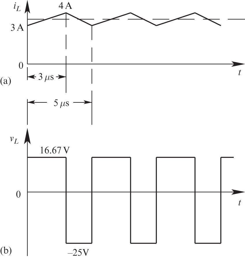
Therefore, the inductor voltage waveform is as shown in Figure 3.3b.
Solution During the current rise time, ![]() Therefore,
Therefore,
During the current fall time, ![]() Hence,
Hence,
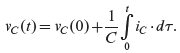
The above analysis applies to any inductor in a switch-mode converter circuit operating in a DC steady state. By analogy, a similar analysis applies to any capacitor in a switch-mode converter circuit operating in the DC steady state as follows: The capacitor voltage and current are related by the conventional differential equation, which can be expressed in the integral form as follows:
where ![]() is a variable of integration representing time. Using the integral form of Equation (3.5), the capacitor voltage at a time
is a variable of integration representing time. Using the integral form of Equation (3.5), the capacitor voltage at a time ![]() can be expressed in terms of its initial value
can be expressed in terms of its initial value ![]() as:
as:
 (3.6)
(3.6)
In the DC steady state, the waveforms of all circuit variables must repeat with the switching frequency time period ![]() , resulting in the following conclusions from Equation (3.6):
, resulting in the following conclusions from Equation (3.6):
- The capacitor voltage waveform repeats with
 , and therefore in Equation (3.6)
 (3.7)
(3.7)
- Integrating over one switching time period
 in Equation (3.6) and using Equation (3.7) show that the capacitor current integral over
  is zero, which leads to the conclusion that the average capacitor current, averaged over
  , is zero:
 (3.8)
(3.8)
The capacitor current ![]() , shown in Figure 3.4a, is flowing through a
, shown in Figure 3.4a, is flowing through a ![]() capacitor. Calculate the peak-peak ripple in the capacitor voltage waveform due to this ripple current.
capacitor. Calculate the peak-peak ripple in the capacitor voltage waveform due to this ripple current.

Solution For the given capacitor current waveform, the capacitor voltage waveform, as shown in Figure 3.4b, is at its minimum at time ![]() , before which the capacitor current has been negative. This voltage waveform reaches its peak at time
, before which the capacitor current has been negative. This voltage waveform reaches its peak at time ![]() , beyond which the current becomes negative.
, beyond which the current becomes negative.
The hatched area in Figure 3.4a equals the charge  .
.
Using Equation (3.6), the peak-peak ripple in the capacitor voltage is ![]() .
.
In addition to the above two conclusions, it is important to recognize that in DC steady state, just as with instantaneous quantities, Kirchhoff’s voltage and current laws apply to average quantities as well. In the DC steady state, average voltages sum to zero in a circuit loop, and average currents sum to zero at a node:
3.3 SIMPLIFYING ASSUMPTIONS
To gain a clear understanding of the DC steady state, we will first make certain simplifying assumptions by ignoring the second-order effects listed below, and later on, we will include them for accuracy:
- Transistors, diodes, and other passive components are all ideal unless explicitly stated. For example, we will ignore the inductor equivalent series resistance.
- The input is a pure DC voltage
 .
. - Design specifications require the ripple in the output voltage to be very small. Therefore, we will initially assume that the output voltage is purely DC without any ripple, that is
 , and later calculate the ripple in it.
 - The current at the current port of the power pole through the series inductor flows continuously, resulting in a continuous conduction mode, CCM (the discontinuous conduction mode, DCM, is analyzed later on).
It is, of course, possible to analyze a switching circuit in detail without making the above simplifying assumptions, as we will do in LTspice-based computer simulations. However, the two-step approach followed here, where the analysis is first carried out by neglecting the second-order effects and adding them later on, provides a deeper insight into converter operation and the design trade-offs.
3.4 COMMON OPERATING PRINCIPLES
In all three converters that we will analyze, the inductor associated with the switching power-pole acts as an energy transfer means from the input to the output. Turning on the transistor of the power pole increases the inductor energy by a certain amount, drawn from the input source, which is transferred to the output stage during the off interval of the transistor. In addition to this inductive energy-transfer means, depending on the converter, there may be additional energy transfer directly from the input to the output, as discussed in the following sections.
3.5 BUCK CONVERTER SWITCHING ANALYSIS IN DC STEADY STATE
A buck converter is shown in Figure 3.5a, with the transistor and the diode making up the bi-positional switch of the power pole. The equivalent series resistance (ESR) of the capacitor will be ignored. Turning on the transistor increases the inductor current in the sub-circuit of Figure 3.5b. When the transistor is turned off, the inductor current freewheels through the diode, as shown in Figure 3.5c.

FIGURE 3.5 Buck DC-DC converter.
For a given transistor switching function waveform ![]() shown in Figure 3.5d with a switch duty ratio
shown in Figure 3.5d with a switch duty ratio ![]() in steady state, the waveform of the voltage
in steady state, the waveform of the voltage ![]() at the current port follows
at the current port follows ![]() as shown. In Figure 3.5d, integrating
as shown. In Figure 3.5d, integrating ![]() over
over ![]() , the average voltage
, the average voltage ![]() equals
equals ![]() . Recognizing that the average inductor voltage is zero (Equations 3.4) and the average voltages in the output loop sum to zero (Equations 3.9),
. Recognizing that the average inductor voltage is zero (Equations 3.4) and the average voltages in the output loop sum to zero (Equations 3.9),
The inductor voltage ![]() pulsates between two values,
pulsates between two values, ![]() and
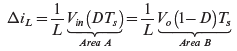
and ![]() , as plotted in Figure 3.5d. Since the average inductor voltage is zero, the volt-second areas during two subintervals are equal in magnitude and opposite in sign. In DC steady state, the inductor current can be expressed as the sum of its average and the ripple component:
, as plotted in Figure 3.5d. Since the average inductor voltage is zero, the volt-second areas during two subintervals are equal in magnitude and opposite in sign. In DC steady state, the inductor current can be expressed as the sum of its average and the ripple component:
where the average current depends on the output load, and the ripple component is dictated by the waveform of the inductor voltage ![]() in Figure 3.5d. As shown in Figure 3.5d, the ripple component consists of linear segments, rising when
in Figure 3.5d. As shown in Figure 3.5d, the ripple component consists of linear segments, rising when ![]() is positive and falling when
is positive and falling when ![]() is negative. The peak-peak ripple can be calculated as follows, using either area A or B:
is negative. The peak-peak ripple can be calculated as follows, using either area A or B:
This ripple component is plotted in Figure 3.5d. Since the average capacitor current is zero in DC steady state, the average inductor current equals the output load current by Kirchhoff’s current law applied at the output node:
The inductor current waveform is shown in Figure 3.5d by superposing the average and the ripple components.
Next, we will calculate the ripple current through the output capacitor. In practice, the filter capacitor is large enough to achieve the output voltage, nearly DC ![]() . Therefore, to the ripple-frequency current, the path through the capacitor offers much smaller impedance than through the load resistance, hence justifying the assumption that the ripple component of the inductor current flows entirely through the capacitor. That is, in Figure 3.5a,
. Therefore, to the ripple-frequency current, the path through the capacitor offers much smaller impedance than through the load resistance, hence justifying the assumption that the ripple component of the inductor current flows entirely through the capacitor. That is, in Figure 3.5a,
In practice, in a capacitor, the voltage drops across its equivalent series resistance (ESR) and the equivalent series inductance (ESL) dominate over the voltage drop ![]() across C, given by Equation (3.6). The capacitor current
across C, given by Equation (3.6). The capacitor current ![]() , equal to
, equal to ![]() in Figure 3.5d, can be used to calculate the ripple in the output voltage.
in Figure 3.5d, can be used to calculate the ripple in the output voltage.
The input current ![]() pulsates, equal to
pulsates, equal to ![]() when the transistor is on, and otherwise zero, as plotted in Figure 3.5d. An input L-C filter is often needed to prevent the pulsating current from being drawn from the input DC source. The average value of the input current in Figure 3.5d is
when the transistor is on, and otherwise zero, as plotted in Figure 3.5d. An input L-C filter is often needed to prevent the pulsating current from being drawn from the input DC source. The average value of the input current in Figure 3.5d is
Using Equations (3.11) and (3.16), we can confirm that the input power equals the output power, as it should, in this idealized converter:
Equation (3.11) shows that the voltage conversion ratio of buck converters in the continuous conduction mode (CCM) depends on D but is independent of the output load. If the output load decreases (that is, if the load resistance increases) to the extent that the inductor current becomes discontinuous, then the input-output relationship in CCM is no longer valid, and, if the duty ratio ![]() were to be held constant, the output voltage in the discontinuous conduction mode would rise above that given by Equation (3.11). The discontinuous conduction mode will be considered fully in section 3.15.
were to be held constant, the output voltage in the discontinuous conduction mode would rise above that given by Equation (3.11). The discontinuous conduction mode will be considered fully in section 3.15.
In the buck DC-DC converter shown in Figure 3.5a, ![]() . It is operating in DC steady state under the following conditions:
. It is operating in DC steady state under the following conditions: ![]() ,
, ![]() ,
, ![]() , and
, and ![]() . Assuming ideal components, calculate and draw the waveforms shown earlier in Figure 3.5d.
. Assuming ideal components, calculate and draw the waveforms shown earlier in Figure 3.5d.
Solution With ![]() ,
, ![]() and
and ![]() ,
, ![]() .
.
The inductor voltage ![]() fluctuates between
fluctuates between ![]() and
and ![]() , as shown in Figure 3.6.
, as shown in Figure 3.6.

Therefore, from Equation (3.13), the ripple in the inductor current is ![]() . The average inductor current is
. The average inductor current is ![]() . Therefore,
. Therefore, ![]() , as shown in Figure 3.6. When the transistor is on,
, as shown in Figure 3.6. When the transistor is on, ![]() , and otherwise it zero. The average input currents is
, and otherwise it zero. The average input currents is ![]() .
.
3.5.1 Simulation and Hardware Prototyping
The simulation of a non-ideal buck converter is demonstrated by means of an example:
Example 3.4
In the buck DC-DC converter shown in Figure 3.5a, ![]() ,
, ![]() , and
, and ![]() . It is operating in DC steady state under the following conditions:
. It is operating in DC steady state under the following conditions: ![]() ,
, ![]() , and
, and ![]() . For the switch and the diode, use the parameters given in the Appendix of Chapter 2. Simulate this converter using LTspice.
. For the switch and the diode, use the parameters given in the Appendix of Chapter 2. Simulate this converter using LTspice.
Solution The simulation file used in this example is available on the accompanying website. The LTspice model is shown in Figure 3.7, and the steady-state waveforms from the simulation of this converter are shown in Figure 3.8.

FIGURE 3.7 LTspice model.

FIGURE 3.8 LTspice simulation results
The Workbench model for implementing the above example in hardware using the Sciamble lab kit is as shown in Figure 3.9.

FIGURE 3.9 Workbench model.
The steady-state waveforms from running the buck converter using the Sciamble laboratory kit are shown in Figure 3.10. The step-by-step procedure for re-creating the above hardware implementation is presented in [2].

FIGURE 3.10 Workbench hardware results: (1) inductor current, (2) switch-node voltage, (3) input current, and (4) output voltage.
3.6 BOOST CONVERTER SWITCHING ANALYSIS IN DC STEADY STATE
A Boost converter is shown in Figure 3.11a. It is conventional to show power flow from left to right. To follow this convention, the circuit of Figure 3.11a is flipped and drawn in Figure 3.11b. The output stage consists of the output load and a large filter capacitor that is used to minimize the output voltage ripple. This capacitor at the output initially gets charged to a voltage equal to ![]() through the diode.
through the diode.

FIGURE 3.11 Boost DC-DC converter.
Compared to buck converters, the boost converters have two major differences:
- Power flow is from a lower voltage DC input to the higher load voltage in the opposite direction through the switching power-pole. Hence, the current direction through the series inductor of the power pole is chosen as shown, opposite to that in a buck converter, and this current remains positive in the continuous conduction mode.
- In the switching power-pole, the bi-positional switch is realized using a transistor and a diode that are placed as shown in Figure 3.7a. Across the output, a filter capacitor
 is placed, which forms the voltage port and minimizes the output ripple voltage.
In a boost converter, turning on the transistor in the bottom position applies the input voltage across the inductor such that ![]() equals
equals ![]() , as shown in Figure 3.12a, and
, as shown in Figure 3.12a, and ![]() linearly ramps up, increasing the energy in the inductor. Turning off the transistor forces the inductor current to flow through the diode, as shown in Figure 3.12b, and some of the inductively stored energy is transferred to the output stage that consists of the filter capacitor and the output load across it.
linearly ramps up, increasing the energy in the inductor. Turning off the transistor forces the inductor current to flow through the diode, as shown in Figure 3.12b, and some of the inductively stored energy is transferred to the output stage that consists of the filter capacitor and the output load across it.

FIGURE 3.12 Boost converter: operation and waveforms.
The transistor switching function is shown in Figure 3.12c, with a steady-state duty ratio ![]() . Because of the transistor in the bottom position in the power pole, the resulting
. Because of the transistor in the bottom position in the power pole, the resulting ![]() waveform is as plotted in Figure 3.12c. Since the average voltage across the inductor in the DC steady state is zero, the average voltage
waveform is as plotted in Figure 3.12c. Since the average voltage across the inductor in the DC steady state is zero, the average voltage ![]() equals the input voltage
equals the input voltage ![]() . The inductor voltage
. The inductor voltage ![]() pulsates between two values:
pulsates between two values: ![]() and
and ![]() as plotted in Figure 3.12c. Since the average inductor voltage is zero, the volt-second areas during the two subintervals are equal in magnitude and opposite in sign.
as plotted in Figure 3.12c. Since the average inductor voltage is zero, the volt-second areas during the two subintervals are equal in magnitude and opposite in sign.
The input/output voltage ratio can be obtained either by the waveform of ![]() or
or ![]() in Figure 3.12c. Using the inductor voltage waveform whose average is zero in DC steady state,
in Figure 3.12c. Using the inductor voltage waveform whose average is zero in DC steady state,
Hence,
The inductor current waveform consists of its average value, which depends on the output load, and a ripple component, which depends on ![]() :
:
where as shown in Figure 3.12c, ![]() , whose average value is zero, consists of linear segments, rising when
, whose average value is zero, consists of linear segments, rising when ![]() is positive and falling when
is positive and falling when ![]() is negative. The peak-peak ripple can be calculated by using either area A or B:
is negative. The peak-peak ripple can be calculated by using either area A or B:
In a boost converter, the inductor current equals the input current, whose average can be calculated from the output load current by equating the input and the output powers:
Hence, using Equation (3.19) and ![]() ,
,
The inductor current waveform is shown in Figure 3.12c, superposing its average and the ripple components.
The current through the diode equals ![]() when the transistor is on; otherwise, it equals
when the transistor is on; otherwise, it equals ![]() , as plotted in Figure 3.12c. In the DC steady state, the average capacitor current
, as plotted in Figure 3.12c. In the DC steady state, the average capacitor current ![]() is zero, and therefore the average diode current equals the output current
is zero, and therefore the average diode current equals the output current ![]() . In practice, the filter capacitor is large to achieve the output voltage of nearly DC
. In practice, the filter capacitor is large to achieve the output voltage of nearly DC ![]() . Therefore, to the ripple-frequency component in the diode current, the path through the capacitor offers a much smaller impedance than through the load resistance, hence justifying the assumption that the ripple component of the diode current flows entirely through the capacitor. That is,
. Therefore, to the ripple-frequency component in the diode current, the path through the capacitor offers a much smaller impedance than through the load resistance, hence justifying the assumption that the ripple component of the diode current flows entirely through the capacitor. That is,
In practice, the voltage drops across the capacitor ESR and the ESL dominate over the voltage drop ![]() across C. The plot of
across C. The plot of ![]() in Figure 3.8c can be used to calculate the ripple in the output voltage.
in Figure 3.8c can be used to calculate the ripple in the output voltage.
In a boost converter, shown in Figure 3.11b, the inductor current has ![]() . It is operating in DC steady state under the following conditions:
. It is operating in DC steady state under the following conditions: ![]() ,
, ![]() ,
, ![]() , and
, and ![]() . (a) Assuming ideal components, calculate
. (a) Assuming ideal components, calculate ![]() and draw the waveforms as shown in Figure 3.12c.
and draw the waveforms as shown in Figure 3.12c.
Solution From Equation (3.19), the duty ratio ![]() . With
. With ![]() ,
, ![]() and
and ![]() .
. ![]() fluctuates between
fluctuates between ![]() and
and ![]() . Using the conditions during the transistor on-time, from Equation (3.21),
. Using the conditions during the transistor on-time, from Equation (3.21),
The average inductor current is ![]() , and
, and ![]() , as shown in Figure 3.13. When the transistor is on, the diode current is zero; otherwise
, as shown in Figure 3.13. When the transistor is on, the diode current is zero; otherwise ![]() . The average diode current is equal to the average output current:
. The average diode current is equal to the average output current:

The capacitor current is ![]() . When the transistor is on, the diode current is zero and
. When the transistor is on, the diode current is zero and ![]() A. The capacitor current jumps to a value of
A. The capacitor current jumps to a value of ![]() and drops to
and drops to ![]() .
.
The above analysis shows that the voltage conversion ratio (Equation 3.19) of boost converters in CCM depends on ![]() , and is independent of the output load, as shown in Figure 3.14. If the output load decreases to the extent that the average inductor current becomes less than the critical value
, and is independent of the output load, as shown in Figure 3.14. If the output load decreases to the extent that the average inductor current becomes less than the critical value ![]() , the inductor current becomes discontinuous, and in this discontinuous conduction mode (DCM), the input-output relationship of CCM is no longer valid, as shown in Figure 3.14.
, the inductor current becomes discontinuous, and in this discontinuous conduction mode (DCM), the input-output relationship of CCM is no longer valid, as shown in Figure 3.14.

FIGURE 3.14 Boost converter: voltage transfer ratio.
If the duty ratio ![]() were to be held constant, as shown in Figure 3.14, the output voltage could rise to dangerously high levels in DCM; this case is fully considered in Section 3.15.
were to be held constant, as shown in Figure 3.14, the output voltage could rise to dangerously high levels in DCM; this case is fully considered in Section 3.15.
3.6.1 Simulation and Hardware Prototyping
The simulation of a non-ideal boost converter is demonstrated by means of an example:
Example 3.6
In the boost DC-DC converter shown in Figure 3.11b, ![]() ,
, ![]() , and
, and ![]() . It is operating in DC steady state under the following conditions:
. It is operating in DC steady state under the following conditions: ![]() ,
, ![]() , and
, and ![]() . For the switch and the diode, use the parameters given in the Appendix of Chapter 2. Simulate this converter using LTspice.
. For the switch and the diode, use the parameters given in the Appendix of Chapter 2. Simulate this converter using LTspice.
Solution The simulation file used in this example is available on the accompanying website. The LTspice model is shown in Figure 3.15, and the steady-state waveforms from the simulation of this converter are shown in Figure 3.16.
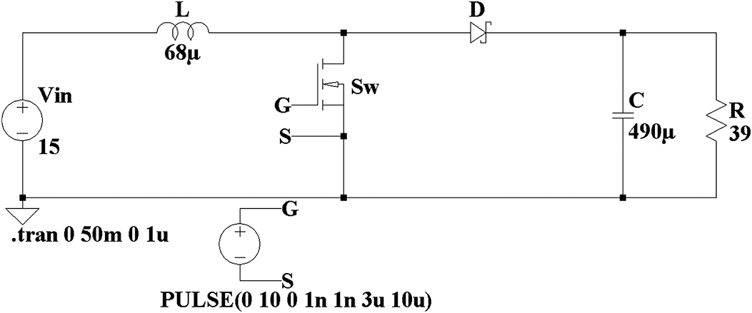
FIGURE 3.15 LTspice model.

FIGURE 3.16 LTspice simulation results.
The Workbench model for implementing the above example in hardware using the Sciamble lab kit is shown in Figure 3.17.

FIGURE 3.17 Workbench model.
The steady-state waveforms from running the boost converter using the Sciamble laboratory kit are shown in Figure 3.18. The step-by-step procedure for re-creating the above hardware implementation is presented in [3].
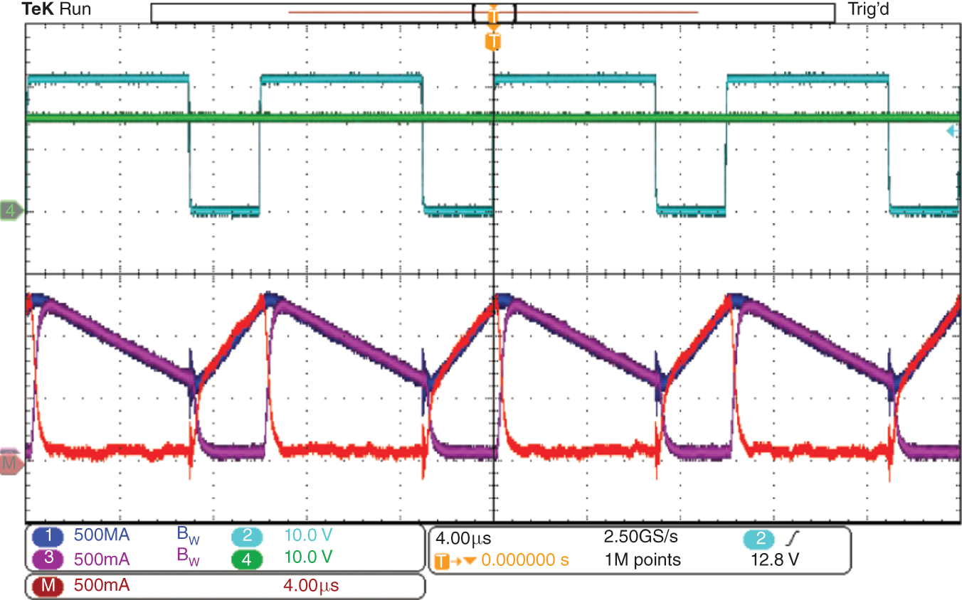
FIGURE 3.18 Workbench hardware results: (1) input current, (2) switch-node voltage, (3) diode current, (4) output voltage, and (M) switch current.
3.7 BUCK-BOOST CONVERTER ANALYSIS IN DC STEADY STATE
Buck-boost converters allow the output voltage to be greater or lower than the input voltage based on the switch duty ratio ![]() . A buck-boost converter is shown in Figure 3.19a, where the switching power-pole is implemented as shown. Conventionally, to make the power flow from left to right, buck-boost converters are drawn as in Figure 3.19b.
. A buck-boost converter is shown in Figure 3.19a, where the switching power-pole is implemented as shown. Conventionally, to make the power flow from left to right, buck-boost converters are drawn as in Figure 3.19b.

FIGURE 3.19 Buck-boost DC-DC converter.
As shown in Figure 3.20a, turning on the transistor applies the input voltage across the inductor such that ![]() equals
equals ![]() , and the current linearly ramps up, increasing the energy in the inductor. Turning off the transistor results in the inductor current flowing through the diode, as shown in Figure 3.20b, transferring to the output the incremental energy in the inductor which was accumulated during the previous transistor state.
, and the current linearly ramps up, increasing the energy in the inductor. Turning off the transistor results in the inductor current flowing through the diode, as shown in Figure 3.20b, transferring to the output the incremental energy in the inductor which was accumulated during the previous transistor state.

FIGURE 3.20 Buck-boost converter: operation and waveforms.
The transistor-switching function is shown in Figure 3.20c, with a steady-state duty ratio ![]() . The resulting
. The resulting ![]() waveform is as plotted. Since the average voltage across the inductor in the DC steady state is zero, the average
waveform is as plotted. Since the average voltage across the inductor in the DC steady state is zero, the average ![]() equals the output voltage
equals the output voltage ![]() . The inductor voltage pulsates between two values:
. The inductor voltage pulsates between two values: ![]() and
and ![]() , as plotted in Figure 3.20c. Since the average inductor voltage is zero, the volt-second areas during the two subintervals are equal in magnitude and opposite in sign.
, as plotted in Figure 3.20c. Since the average inductor voltage is zero, the volt-second areas during the two subintervals are equal in magnitude and opposite in sign.
The input/output voltage ratio can be obtained either by the waveform of ![]() or
or ![]() in Figure 3.20c. Using the
in Figure 3.20c. Using the ![]() waveform, whose average is zero in the DC steady state,
waveform, whose average is zero in the DC steady state,
Hence,
The inductor current consists of an average value, which depends on the output load, and a ripple component, which depends on ![]() :
:
where as shown in Figure 3.20c, ![]() , whose average value is zero, consists of linear segments, rising when
, whose average value is zero, consists of linear segments, rising when ![]() is positive and falling when
is positive and falling when ![]() is negative. The peak-peak ripple can be calculated by using either area A or B,
is negative. The peak-peak ripple can be calculated by using either area A or B,
 (3.28)
Applying Kirchhoff’s current law in Figure 3.19a or 3.19b, the average inductor current equals the sum of the average input current and the average output current (note that the average capacitor current is zero in DC steady state),
Equating the input and the output powers,
and using Equation (3.26),
Hence, using Equations (3.29) and (3.31),
Superposing the average and the ripple components, the inductor current waveform is shown in Figure 3.20c.
The diode current is zero, except when it conducts the inductor current, as plotted in Figure 3.20c. In the DC steady state, the average current ![]() through the capacitor is zero, and therefore by Kirchhoff’s current law, the average diode current equals the output current. In practice, the filter capacitor is large to achieve the output voltage nearly DC
through the capacitor is zero, and therefore by Kirchhoff’s current law, the average diode current equals the output current. In practice, the filter capacitor is large to achieve the output voltage nearly DC ![]() . Therefore, to the ripple-frequency current, the path through the capacitor offers a much smaller impedance than through the load resistance, hence justifying the assumption that the ripple component of the diode current flows entirely through the capacitor. That is,
. Therefore, to the ripple-frequency current, the path through the capacitor offers a much smaller impedance than through the load resistance, hence justifying the assumption that the ripple component of the diode current flows entirely through the capacitor. That is,
In practice, the voltage drops across the capacitor ESR and the ESL dominate over the voltage drop ![]() across C. The plot of
across C. The plot of ![]() in Figure 3.20c can be used to calculate the ripple in the output voltage.
in Figure 3.20c can be used to calculate the ripple in the output voltage.
The buck-boost converter of Figure 3.19b is operating in DC steady state under the following conditions: ![]() ,
, ![]() ,
, ![]() ,
, ![]() , and
, and ![]() . Assuming ideal components, calculate
. Assuming ideal components, calculate ![]() and draw the waveforms as shown in Figure 3.20c.
and draw the waveforms as shown in Figure 3.20c.
Solution From Equation (3.26), ![]() .
. ![]() and
and ![]() , as shown in Figure 3.13. The inductor voltage
, as shown in Figure 3.13. The inductor voltage ![]() fluctuates between
fluctuates between ![]() and
and ![]() . Using Equation (3.28),
. Using Equation (3.28),
The average input current is ![]() , and
, and ![]() . Therefore,
. Therefore, ![]() . When the transistor is on, the diode current is zero; otherwise,
. When the transistor is on, the diode current is zero; otherwise, ![]() . The average diode current is equal to the average output current:
. The average diode current is equal to the average output current: ![]() . The capacitor current is
. The capacitor current is ![]() . When the transistor is on, the diode current is zero and
. When the transistor is on, the diode current is zero and ![]() . The capacitor current jumps to a value of
. The capacitor current jumps to a value of ![]() and drops to
and drops to ![]() , as shown in Figure 3.21.
, as shown in Figure 3.21.

The above analysis shows that the voltage conversion ratio (Equation 3.26) of buck-boost converters in CCM depends on ![]() and is independent of the output load, as shown in Figure 3.22. If the output load decreases to the extent that the average inductor current becomes less than the critical value
and is independent of the output load, as shown in Figure 3.22. If the output load decreases to the extent that the average inductor current becomes less than the critical value ![]() , the inductor current becomes discontinuous, and in this discontinuous conduction mode (DCM), the input-output relationship of CCM is no longer valid, as shown in Figure 3.22. If the duty ratio
, the inductor current becomes discontinuous, and in this discontinuous conduction mode (DCM), the input-output relationship of CCM is no longer valid, as shown in Figure 3.22. If the duty ratio ![]() were to be held constant as shown in Figure 3.22, the output voltage could rise to dangerously high levels in DCM; this case is fully considered in Section 3.23.
were to be held constant as shown in Figure 3.22, the output voltage could rise to dangerously high levels in DCM; this case is fully considered in Section 3.23.

FIGURE 3.22 Buck-boost converter: voltage transfer ratio.
3.7.1 Simulation and Hardware Prototyping
The simulation of a non-ideal buck-boost converter is demonstrated by means of an example:
Example 3.8
In the buck-boost DC-DC converter shown in Figure 3.19b, ![]() ,
, ![]() , and
, and ![]() . It is operating in DC steady state under the following conditions:
. It is operating in DC steady state under the following conditions: ![]() ,
, ![]() , and
, and ![]() . For the switch and the diode, use the parameters given in the Appendix of Chapter 2. Simulate this converter using LTspice.
. For the switch and the diode, use the parameters given in the Appendix of Chapter 2. Simulate this converter using LTspice.
Solution The simulation file used in this example is available on the accompanying website. The LTspice model is shown in Figure 3.23, and the steady-state waveforms from the simulation of this converter are shown in Figure 3.24.

FIGURE 3.23 LTspice model.
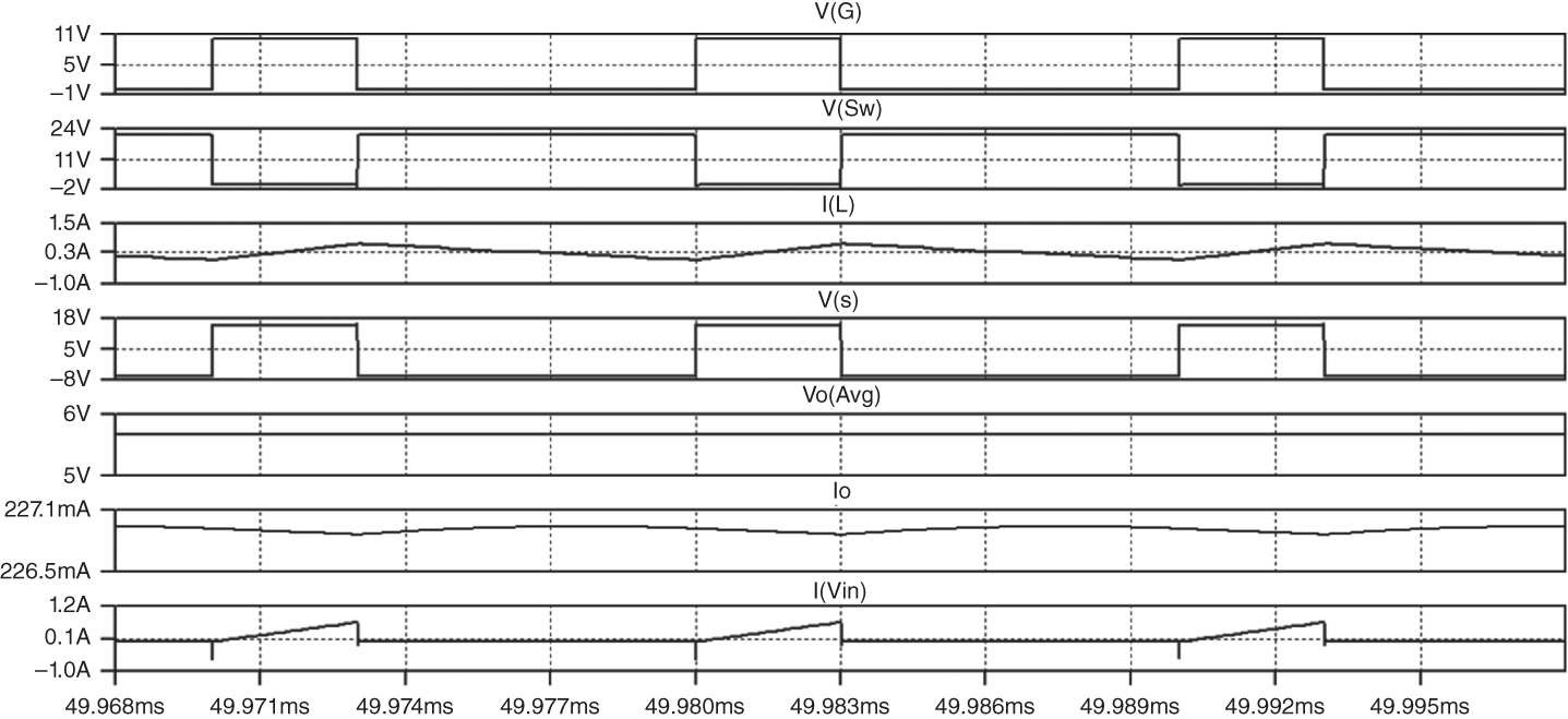
FIGURE 3.24 LTspice simulation results..
The Workbench model for implementing the above example in hardware using the Sciamble lab kit is as shown in Figure 3.25.
FIGURE 3.25 Workbench model.
The steady-state waveforms from running the buck-boost converter using the Sciamble laboratory kit are shown in Figure 3-26. The step-by-step procedure for re-creating the above hardware implementation is presented in [4].
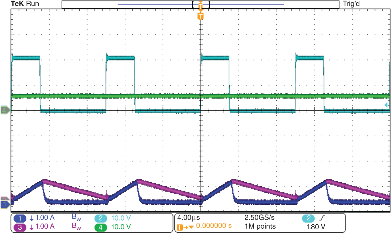
FIGURE 3.26 Workbench hardware results: (1) input current, (2) switch-node voltage, (3) inductor current, and (4) output voltage.
3.7.2 Other Buck-Boost Topologies
There are two variations of the buck-boost topology, which are used in certain applications. These two topologies are briefly described below.
3.7.2.1 SEPIC Converters (Single-Ended Primary Inductor Converters)
The SEPIC converter, shown in Figure 3.27a, is used in certain applications where the current drawn from the input is required to be relatively ripple-free. By applying Kirchhoff’s voltage law and the fact that the average inductor voltage is zero in the DC steady state, the capacitor in this converter gets charged to an average value that equals the input voltage ![]() with the polarity shown. During the on interval of the transistor,
with the polarity shown. During the on interval of the transistor, ![]() , as shown in Figure 3.27b, the diode gets reverse biased by the sum of the capacitor and the output voltages, and
, as shown in Figure 3.27b, the diode gets reverse biased by the sum of the capacitor and the output voltages, and ![]() and
and ![]() flow through the transistor. During the off interval
flow through the transistor. During the off interval ![]() ,
, ![]() and
and ![]() flow through the diode, as shown in Figure 3.15c. The voltage across
flow through the diode, as shown in Figure 3.15c. The voltage across ![]() equals
equals ![]() during the on interval and (
during the on interval and (![]() ) during the off interval. In terms of the average value of the capacitor voltage that equals
) during the off interval. In terms of the average value of the capacitor voltage that equals ![]() (by applying Equation (3.9) in Figure 3.27a), equating the average voltage across
(by applying Equation (3.9) in Figure 3.27a), equating the average voltage across ![]() to zero results in,
to zero results in,

FIGURE 3.27 SEPIC converter.
or
Unlike the buck-boost converters, the output voltage polarity in the SEPIC converter remains the same as that of the input.
3.7.2.2 Ćuk Converters
Named after its inventor, the Ćuk converter is shown in Figure 3.28a, where the energy transfer means is through the capacitor ![]() between the two inductors. Using Equation (3.9) in Figure 3.28a, this capacitor voltage has an average value of
between the two inductors. Using Equation (3.9) in Figure 3.28a, this capacitor voltage has an average value of ![]() with the polarity shown. During the on interval of the transistor,
with the polarity shown. During the on interval of the transistor, ![]() , as shown in Figure 3.28b, the diode gets reverse biased by the capacitor voltage, and the input and the output currents flow through the transistor. During the off interval
, as shown in Figure 3.28b, the diode gets reverse biased by the capacitor voltage, and the input and the output currents flow through the transistor. During the off interval ![]() , the input and the output currents flow through the diode, as shown in Figure 3.28c. In terms of the average values of the inductor currents, equating the net change in charge on the capacitor over
, the input and the output currents flow through the diode, as shown in Figure 3.28c. In terms of the average values of the inductor currents, equating the net change in charge on the capacitor over ![]() to zero in steady state,
to zero in steady state,
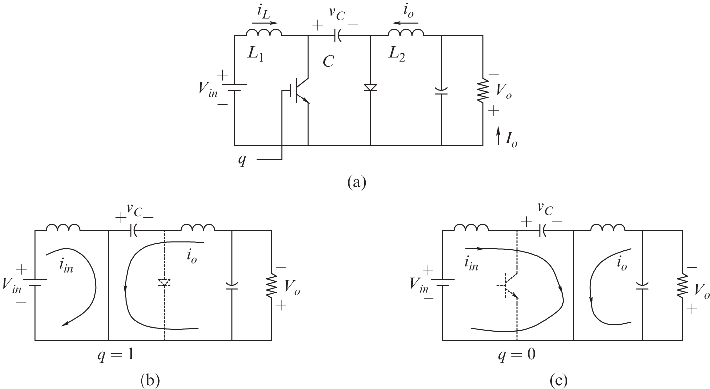
FIGURE 3.28 Ćuk converter.
or
Equating input and output powers in this idealized converter leads to,
which shows the same functionality as buck-boost converters. One of the advantages of the Ćuk converter is that it has non-pulsating currents at the input and the output, but it suffers from the same component stress disadvantages as the buck-boost converters and produces an output voltage of the polarity opposite to that of the input.
3.8 TOPOLOGY SELECTION [5]
For selecting between the three converter topologies discussed in this chapter, the stresses listed in Table 3.1 can be compared, which are based on the assumption that the inductor ripple current is negligible.
TABLE 3.1 Topology selection criteria.
| Criterion | Buck | Boost | Buck-boost | |
|---|---|---|---|---|
| Transistor | ||||
| Transistor | ||||
| Transistor | ||||
|
| Transistor | |||
| Diode | ||||
|
| ||||
| Effect of | significant | little | little | |
| Pulsating Current | input | output | both | |
From the above table, we can clearly conclude that the buck-boost converter suffers from several additional stresses. Therefore, it should be used only if both the buck and the boost capabilities are needed. Otherwise, the buck or the boost converter should be used based on the desired capability. A detailed analysis is carried out in [2].
3.9 WORST-CASE DESIGN
The worst-case design should consider the ranges in which the input voltage and the output load vary. As mentioned earlier, converters above a few tens of watts are often designed to operate in CCM. To ensure CCM even under very light load conditions would require prohibitively large inductance. Hence, the inductance value chosen is often no larger than three times the critical inductance ![]() , where the critical inductance
, where the critical inductance ![]() is the value of the inductor that will make the converter operate at the border of CCM and DCM at full load.
is the value of the inductor that will make the converter operate at the border of CCM and DCM at full load.
3.10 SYNCHRONOUS-RECTIFIED BUCK CONVERTER FOR VERY LOW OUTPUT VOLTAGES [6]
Operating voltages in computing and communication equipment have already dropped to an order of 1 V, and even lower voltages, such as 0.5 V, are predicted in the near future. At these low voltages, the diode (even a Schottky diode) of the power pole in a buck converter has an unacceptably high voltage drop across it, resulting in extremely poor converter efficiency.
As a solution to this problem, the switching power-pole in a buck converter is implemented using two MOSFETs, as shown in Figure 3.29a, which are available with very low ![]() in low voltage ratings. The two MOSFETs are driven by almost complementary gate signals (some dead time, where both signals are low, is necessary to avoid the shoot-through of current through the two transistors), as shown in Figure 3.29b.
in low voltage ratings. The two MOSFETs are driven by almost complementary gate signals (some dead time, where both signals are low, is necessary to avoid the shoot-through of current through the two transistors), as shown in Figure 3.29b.

FIGURE 3.29 Buck converter: synchronous rectified.
When the upper MOSFET is off, the inductor current flows through the channel, from the source to the drain, of the lower MOSFET that has gate voltage applied to it. This results in a very low voltage drop across the lower MOSFET. At light load conditions, the inductor current may be allowed to become negative without becoming discontinuous, flowing from the drain to the source of the lower MOSFET [3].
It is possible to achieve soft switching in such converters, as discussed in Chapter 10, where the ripple in the total output and the input currents can be minimized by interleaving, which is discussed in the next section.
3.10.1 Simulation and Hardware Prototyping
The simulation of a non-ideal synchronous buck converter is demonstrated by means of an example:
Example 3.9
In the synchronous-rectified buck DC-DC converter shown in Figure 3.29a, ![]() ,
, ![]() , and
, and ![]() . It is operating in DC steady state under the following conditions:
. It is operating in DC steady state under the following conditions: ![]() ,
, ![]() , and
, and ![]() . For the switch, use the parameters given in the Appendix of Chapter 2. Simulate this converter using LTspice.
. For the switch, use the parameters given in the Appendix of Chapter 2. Simulate this converter using LTspice.
Solution The simulation file used in this example is available on the accompanying website. The LTspice model is shown in Figure 3.30, and the steady-state waveforms from the simulation of this converter are shown in Figure 3.31.
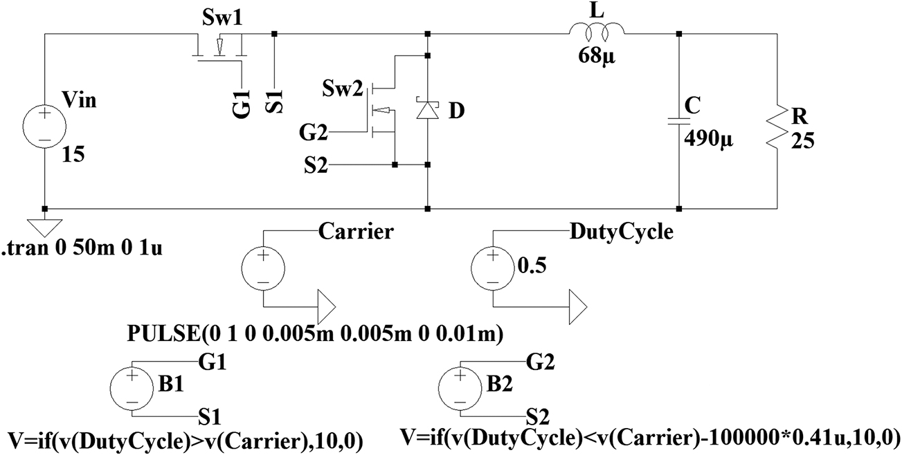
FIGURE 3.30 LTspice model.

FIGURE 3.31 LTspice simulation results.
The Workbench model for implementing the above example in hardware using the Sciamble lab kit is shown in Figure 3.32.

FIGURE 3.32 Workbench model.
The steady-state waveforms from running the synchronous-rectified buck converter using the Sciamble laboratory kit are shown in Figure 3.33. The step-by-step procedure for re-creating the above hardware implementation is presented in [7].

FIGURE 3.33 Workbench hardware results for synchronous-rectified buck converter using Si switches: (1) inductor current, (2) switch-node voltage, (3) high-side switch current/input current, and (M) low-side switch current.
In the case of a buck converter, discussed in section 3.5, there is a significant reduction in the efficiency due to the 0.3–1.1 V drop across the freewheeling diode, as seen in Figure 3.34a. This drop can be greatly reduced in the synchronous-rectified buck converter by using a Si-MOSFET instead of a diode, as seen in Figure 3.34b.

FIGURE 3.34 Switch-node voltage: (a) buck converter, (b) synchronous-rectified buck converter using Si-MOSFETs, (c) synchronous-rectified buck converter using GaN-FETs.
It must be noted that, while the gate ON signal transitions from one MOSFET to the other, both MOSFETs’ gate is held OFF for a brief period of time to prevent shoot-through. During this short interval, the current flows through the body diode of the MOSFET, as seen by the −0.7 V drop during the dead time, of about 200 ns, in Figure 3.34b.
Figure 3.34c shows the switch-node voltage of a synchronous-rectified buck converter using GaN-FETs. The dead time required for GaN-FET of a similar rating as Si-MOSFET is typically an order of magnitude lower, 30 ns in this case. This faster switching characteristic leads to reduced switching losses. Particular care must be taken to ensure that the dead time is maintained as low as possible [8] because the voltage drop across the GaN-FET under reverse current conduction, while the gate is OFF, is typically around 3.5 V, as seen in Figure 3.34c. This reverse voltage drop is significantly higher than that of a Si-MOSFET’s body diode.
3.11 INTERLEAVING OF CONVERTERS
Figure 3.35a shows two interleaved converters whose switching waveforms are phase-shifted by ![]() , as shown in Figure 3.35b. In general, n such converters can be used, their operation phase-shifted by
, as shown in Figure 3.35b. In general, n such converters can be used, their operation phase-shifted by ![]() . The advantage of such interleaved multi-phase converters is the cancellation of ripple in the input and the output currents to a large degree. This is also a good way to achieve higher control bandwidth.
. The advantage of such interleaved multi-phase converters is the cancellation of ripple in the input and the output currents to a large degree. This is also a good way to achieve higher control bandwidth.

FIGURE 3.35 Interleaving of converters.
3.12 REGULATION OF DC-DC CONVERTERS BY PWM
Almost all DC-DC converters are operated with their output voltages regulated to equal their reference values within a specified tolerance band (for example, ![]() around its nominal value) in response to disturbances in the input voltage and the output load. The average output of the switching power-pole in a DC-DC converter can be controlled by pulsed-width modulating (PWM) the duty ratio
around its nominal value) in response to disturbances in the input voltage and the output load. The average output of the switching power-pole in a DC-DC converter can be controlled by pulsed-width modulating (PWM) the duty ratio ![]() of this power pole.
of this power pole.
Figure 3.36a shows a block diagram form of a regulated DC-DC converter. It shows that the converter output voltage is measured and compared with its reference value within a PWM controller IC, briefly described in Chapter 2. The error between the two voltages is amplified by an amplifier, whose output is the control voltage ![]() . Within the PWM-IC, the control voltage is compared with a ramp signal
. Within the PWM-IC, the control voltage is compared with a ramp signal ![]() , as shown in Figure 3.36b, where the comparator output represents the switching function
, as shown in Figure 3.36b, where the comparator output represents the switching function ![]() whose pulse width
whose pulse width ![]() can be modulated to regulate the output of the converter.
can be modulated to regulate the output of the converter.
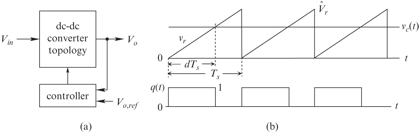
FIGURE 3.36 Regulation of output by PWM.
The ramp signal ![]() has the amplitude
has the amplitude ![]() , and the switching frequency
, and the switching frequency ![]() constant. The output voltage of this comparator represents the transistor-switching function
constant. The output voltage of this comparator represents the transistor-switching function ![]() , which equals 1 if
, which equals 1 if ![]() and 0 otherwise. The switch duty ratio in Figure 3.36b is given as
and 0 otherwise. The switch duty ratio in Figure 3.36b is given as
and thus the control voltage, limited in a range between ![]() and
and ![]() , linearly and dynamically controls the pulse width
, linearly and dynamically controls the pulse width ![]() in Equation (3.39) and shown in Figure 3.36b. The topic of feedback controller design for regulating the output voltage is discussed in detail in Chapter 4.
in Equation (3.39) and shown in Figure 3.36b. The topic of feedback controller design for regulating the output voltage is discussed in detail in Chapter 4.
3.13 DYNAMIC AVERAGE REPRESENTATION OF CONVERTERS IN CCM
In all three types of DC-DC converters in CCM, the switching power-pole switches between two sub-circuit states based on the switching function ![]() . (It switches between three sub-circuit states in DCM, where the switch can be considered “stuck” between the on and the off positions during the subinterval when the inductor current is zero, discussed in detail in Section 3.15.) It is very beneficial to obtain non-switching average models of these switch-mode converters for simulating the converter performance under dynamic conditions caused by the change of input voltage and/or the output load. Under the dynamic condition, the converter duty ratio, and the average values of voltages and currents within the converter vary with time, but relatively slowly, with frequencies an order of magnitude smaller than the switching frequency.
. (It switches between three sub-circuit states in DCM, where the switch can be considered “stuck” between the on and the off positions during the subinterval when the inductor current is zero, discussed in detail in Section 3.15.) It is very beneficial to obtain non-switching average models of these switch-mode converters for simulating the converter performance under dynamic conditions caused by the change of input voltage and/or the output load. Under the dynamic condition, the converter duty ratio, and the average values of voltages and currents within the converter vary with time, but relatively slowly, with frequencies an order of magnitude smaller than the switching frequency.
The switching power-pole is shown in Figure 3.37a, where the voltages and currents are labeled with the subscript ![]() for the voltage port and
for the voltage port and ![]() for the current port. In the above analysis for the three converters in the DC steady state, we can write the average voltage and current relationships for the bi-positional switch of the power pole as,
for the current port. In the above analysis for the three converters in the DC steady state, we can write the average voltage and current relationships for the bi-positional switch of the power pole as,
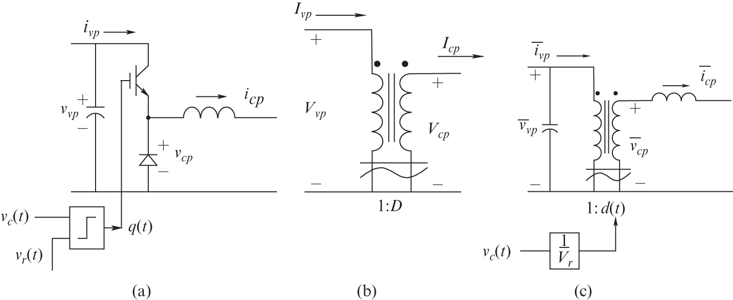
FIGURE 3.37 Average dynamic model of a switching power-pole.
Relationships in Equation (3.40) can be represented by an ideal transformer as shown in Figure 3.37b, where the ideal transformer, hypothetical and only a convenience for mathematical representation, can operate with AC as well DC voltages and currents, which a real transformer cannot. A symbol consisting of a straight bar with a curve below it is used to remind us of this fact. Since no electrical isolation exists between the voltage port and the current port of the switching power-pole, the two windings of this ideal transformer in Figure 3.37b are connected at the bottom. Moreover, the voltage at the voltage port in Figure 3.37b cannot become negative, and ![]() is limited to a range between 0 and 1.
is limited to a range between 0 and 1.
Under dynamic conditions, the average model in Figure 3.37b of the bi-positional switch can be substituted in the power pole of Figure 3.37a, resulting in the dynamic average model shown in Figure 3.37c, using Equation (3.39) for ![]() . Here, the uppercase letters used in the DC steady state relationships are replaced with lowercase letters with an overbar (a “–” on top) to represent average voltages and currents, which may vary dynamically with time:
. Here, the uppercase letters used in the DC steady state relationships are replaced with lowercase letters with an overbar (a “–” on top) to represent average voltages and currents, which may vary dynamically with time: ![]() by
by ![]() ,
, ![]() by
by ![]() ,
, ![]() by
by ![]() , and
, and ![]() by
by ![]() . Therefore, from Equations (3.40a) and (3.40b):
. Therefore, from Equations (3.40a) and (3.40b):
The above discussion shows that the dynamic average model of a switching power-pole in CCM is an ideal transformer with the turns ratio ![]() . Using this model for the switching power-pole, the dynamic average models of the three converters shown in Figure 3.38a are as in Figure 3.38b in CCM. Note that in the boost converter where the transistor is in the bottom position in the power pole, the transformer turns ratio is
. Using this model for the switching power-pole, the dynamic average models of the three converters shown in Figure 3.38a are as in Figure 3.38b in CCM. Note that in the boost converter where the transistor is in the bottom position in the power pole, the transformer turns ratio is ![]() for the following reason: Unlike buck and buck-boost converters, the transistor in a boost converter is in the bottom position. Therefore, when the transistor is on with a duty ratio
for the following reason: Unlike buck and buck-boost converters, the transistor in a boost converter is in the bottom position. Therefore, when the transistor is on with a duty ratio ![]() , the effective bi-positional switch is in the “down” position, and the pole duty ratio is
, the effective bi-positional switch is in the “down” position, and the pole duty ratio is ![]() . The average representation of these converters in DCM is described in section 3.15.5.
. The average representation of these converters in DCM is described in section 3.15.5.

FIGURE 3.38 Average dynamic models: buck (left), boost (middle), and buck-boost (right).
In the average representation of the switching converters, all the switching information is removed, and hence it provides an uncluttered understanding of achieving desired objectives. Moreover, the average model in simulating the dynamic response of a converter results in computation speeds orders of magnitude faster than that in the switching model, where the simulation time-step must be smaller than at least one-hundredth of the switching time period ![]() in order to achieve an accurate resolution.
in order to achieve an accurate resolution.
3.14 BI-DIRECTIONAL SWITCHING POWER-POLE
In buck, boost, and buck-boost DC-DC converters, the implementation of the switching power-pole by one transistor and one diode dictates the instantaneous current flow to be unidirectional. As shown in Figure 3.39a, combining the switching power-pole implementations of buck and boost converters, where the two transistors are switched by complementary signals, allows a continuous bi-directional power and current capability.

FIGURE 3.39 Bi-directional power flow through a switching power-pole.
In such a bi-directional switching power-pole, the positive inductor current, as shown in Figure 3.39b, represents a buck mode, where only the transistor and the diode associated with the buck converter take part. Similarly, as shown in Figure 3.39c, the negative inductor current represents a boost mode, where only the transistor and the diode associated with the boost converter take part. We will utilize such bi-directional switching power-poles in DC and AC motor drives, uninterruptible power supplies, and power systems applications, discussed in Chapters 11 and 12.
In a bi-directional switching power-pole where the transistors are gated by complementary signals, the current through it can flow in either direction, and hence ideally (ignoring a small dead time needed due to practical considerations when both the transistors are off simultaneously for a very short interval), a discontinuous conduction mode does not exist.
As described by Figures 3.39b and c above, the bi-directional switching power-pole in Figure 3.40a is in the “up” position, regardless of the direction of ![]() , when
, when ![]() , as shown in Figure 3.40b. Similarly, it is in the “down” position, regardless of the direction of
, as shown in Figure 3.40b. Similarly, it is in the “down” position, regardless of the direction of ![]() , when
, when ![]() . Therefore, the average representation of the bi-directional switching power-pole in Figure 3.40a (represented as in Figure 3.40b) is an ideal transformer shown in Figure 3.40c, with a turns ratio
. Therefore, the average representation of the bi-directional switching power-pole in Figure 3.40a (represented as in Figure 3.40b) is an ideal transformer shown in Figure 3.40c, with a turns ratio ![]() , where
, where ![]() represents the pole duty ratio that is also the duty ratio of the transistor associated with the buck mode.
represents the pole duty ratio that is also the duty ratio of the transistor associated with the buck mode.
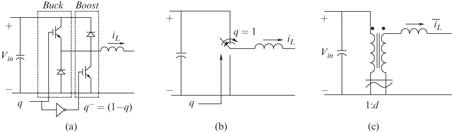
FIGURE 3.40 Average dynamic model of the switching power-pole with bi-directional power flow.
3.15 DISCONTINUOUS-CONDUCTION MODE (DCM)
All DC-DC converters for unidirectional power and current flow have their switching power-pole implemented by one transistor and one diode and hence go into a discontinuous conduction mode, DCM, below a certain output load. As an example, as shown in Figure 3.41, if we keep the switch duty ratio constant, a decline in the output load results in the inductor average current to decrease until a critical load value is reached, where the inductor current waveform reaches zero at the end of the turn-off interval.

FIGURE 3.41 Inductor current at various loads; duty ratio is kept constant.
We will call the average inductor current in this condition the critical inductor current and denote it by ![]() . For loads below this critical value, the inductor current cannot reverse through the diode in any of the three converters (buck, boost, and buck-boost) and enters DCM, where the inductor current remains zero for a finite interval until the transistor is turned on, beginning the next switching cycle.
. For loads below this critical value, the inductor current cannot reverse through the diode in any of the three converters (buck, boost, and buck-boost) and enters DCM, where the inductor current remains zero for a finite interval until the transistor is turned on, beginning the next switching cycle.
In DCM, during the interval when the inductor current remains zero, there is no power drawn from the input source, and there is no energy in the inductor to transfer to the output stage. This interval of inactivity generally results in increased device stresses and the ratings of the passive components. DCM also results in noise and EMI, although the diode reverse recovery problem is minimized. Based on these considerations, converters above a few tens of watts are generally designed to operate in CCM, although all of them implemented using one transistor and one diode will enter DCM at very light loads, and the feedback controller should be designed to operate adequately in both modes. It should be noted that designing the controller of some converters, such as the buck-boost converters, in CCM is more complicated, so the designers may prefer to keep such converters in DCM for all possible operating conditions. This we will discuss further in the next chapter, dealing with the feedback controller design.
3.15.1 Critical Condition at the Border of Continuous-Discontinuous Conduction
At the critical load condition with ![]() shown in Figure 3.41, the average inductor current is one-half the peak value:
shown in Figure 3.41, the average inductor current is one-half the peak value:
At the critical condition, the peak inductor current in Figure 3.41 can be calculated by considering the voltage ![]() that is applied across the inductor for an interval
that is applied across the inductor for an interval ![]() when the transistor is on, causing the current to rise from zero to its peak value. In buck converters, this inductor voltage is
when the transistor is on, causing the current to rise from zero to its peak value. In buck converters, this inductor voltage is ![]() . Using Equation (3.42) and the fact that
. Using Equation (3.42) and the fact that ![]() and
and ![]() (the same voltage relationship holds in the critical condition as in CCM),
(the same voltage relationship holds in the critical condition as in CCM),
In both the boost and the buck-boost converters, the inductor voltage during ![]() equals
equals ![]() . Hence, using Equation (3.42),
. Hence, using Equation (3.42),
Equating the critical values of the average inductor current given in Equations (3.43) and (3.44) to input/output currents, relating the output voltage ![]() to the input voltage
to the input voltage ![]() and recognizing that the output resistance
and recognizing that the output resistance ![]() , the critical values of the load resistance in these converters can be derived as:
, the critical values of the load resistance in these converters can be derived as:
 (3.45)
A load resistance above this critical value results in less than a critical load, causing the corresponding converter to go into DCM.
3.15.2 Buck Converters in DCM in Steady State
Waveforms for a buck converter under DCM are shown in Figure 3.42a. In DCM, the inductor current remains zero for a finite interval, resulting in an average value (equal to ![]() ) that is smaller than the critical value. When the inductor current is zero during the
) that is smaller than the critical value. When the inductor current is zero during the ![]() interval, the voltage across the inductor is zero and
interval, the voltage across the inductor is zero and ![]() .
.
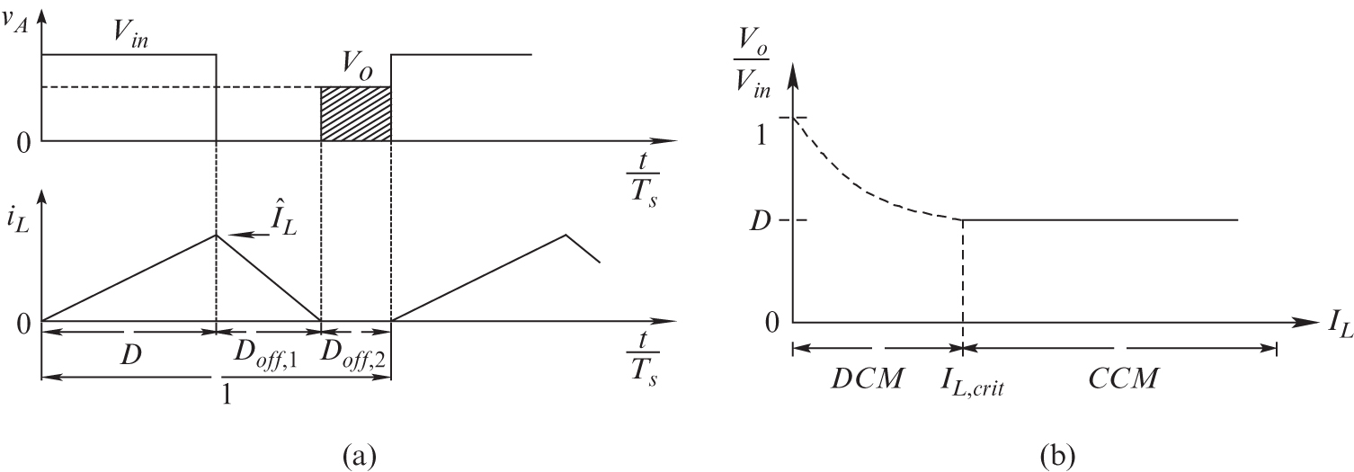
FIGURE 3.42 Buck converter in DCM.
In a buck converter, ![]() equals
equals ![]() during the on interval and is otherwise zero. In Figure 3.42a in DCM,
during the on interval and is otherwise zero. In Figure 3.42a in DCM,
Hence the average value of the input current, recognizing that ![]() ,
,
Equating the average input power ![]() to the output power
to the output power ![]() , we can derive that (see problem 3.32),
, we can derive that (see problem 3.32),
where
Equation (3.48) shows that light loads with ![]() cause the output voltage to rise towards the input voltage, as shown in Figure 3.42b. Of course in a regulated DC-DC converter, the feedback controller will adjust the duty ratio in order to regulate the output voltage.
cause the output voltage to rise towards the input voltage, as shown in Figure 3.42b. Of course in a regulated DC-DC converter, the feedback controller will adjust the duty ratio in order to regulate the output voltage.
3.15.2.1 Simulation and Hardware Prototyping
The simulation of a non-ideal buck converter operating under discontinuous conduction mode is demonstrated by means of an example:
In the buck DC-DC converter shown in Figure 3.5a, ![]() ,
, ![]() , and
, and ![]() . It is operating in DC steady state under the following conditions:
. It is operating in DC steady state under the following conditions: ![]() ,
, ![]() , and
, and ![]() . For the switch and the diode, use the parameters given in the Appendix of Chapter 2. Simulate this converter using LTspice.
. For the switch and the diode, use the parameters given in the Appendix of Chapter 2. Simulate this converter using LTspice.
Solution The simulation file used in this example is available on the accompanying website. The LTspice model is the same as the one shown in Figure 3.7, and the steady-state waveforms from the simulation of this converter are shown in Figure 3.43.

FIGURE 3.43 LTspice simulation results.
The steady-state waveforms from running the buck converter under discontinuous conduction mode using the Sciamble laboratory kit are shown in Figure 3.44. The Workbench model is the same as the one shown in Figure 3.9. The step-by-step procedure for re-creating the above hardware implementation is presented in [9].

FIGURE 3.44 Workbench hardware: (1) inductor current, (2) switch-node voltage, (3) input current, and (4) output voltage.
3.15.2.2 Ringing of the Voltage at the Switching Node
Compared to the operation of the ideal buck converter in Figure 3.5a, the switch node voltage of a practical buck converter during ![]() rings with a peak-to-peak magnitude which is double that of the magnitude of the output voltage, clamped between 0 and Vin
:
rings with a peak-to-peak magnitude which is double that of the magnitude of the output voltage, clamped between 0 and Vin
:![]() . This is due to the LC tank circuit formed by the filter inductor and the parallel combination of switch and diode parasitic capacitance, as shown in Figure 3.45.
. This is due to the LC tank circuit formed by the filter inductor and the parallel combination of switch and diode parasitic capacitance, as shown in Figure 3.45.

FIGURE 3.45 Non-ideal buck converter showing the parasitic switch and diode capacitance.
This ringing leads to increased electromagnetic interference (EMI) and higher losses. Knowing the frequency of this ringing is necessary to design an EMI filter to suppress this frequency component. The procedure is demonstrated by means of an example:
Example 3.11
In the buck converter shown in Figure 3.45, the switch has a parasitic capacitance of ![]() and the diode has a parasitic capacitance of
and the diode has a parasitic capacitance of ![]() . Assume the remaining parameters are the same as those given in Example 3.10. Compute the ringing frequency of the ringing of switching node voltage.
. Assume the remaining parameters are the same as those given in Example 3.10. Compute the ringing frequency of the ringing of switching node voltage.
Solution
This matches the results shown in Figure 3.45. The magnitude and the total time period of this ringing can be greatly reduced by means of a snubber circuit, which is discussed in Chapter 8.
3.15.3 Boost Converters in DCM in Steady State
Waveforms for a boost converter under DCM are shown in Figure 3.46a. In DCM, when the inductor current is zero during the ![]() interval, the voltage across the inductor is zero, and
interval, the voltage across the inductor is zero, and ![]() equals
equals ![]() . In a boost converter, the average
. In a boost converter, the average ![]() , and
, and ![]() equals
equals ![]() during all intervals. In Figure 3.46a in DCM,
during all intervals. In Figure 3.46a in DCM,
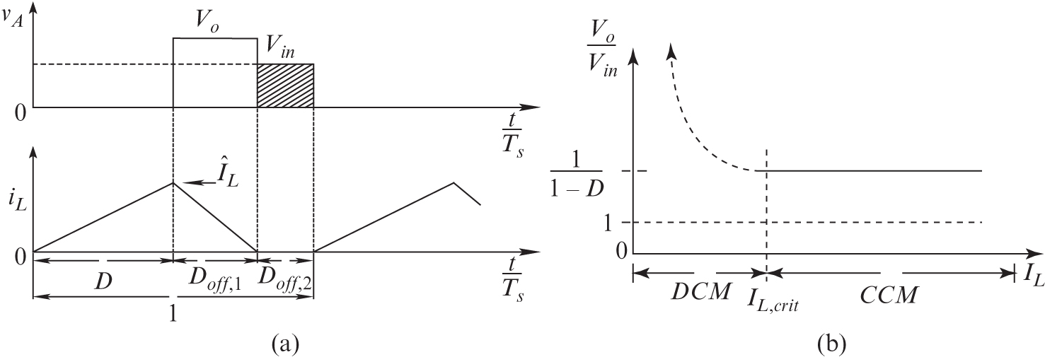
FIGURE 3.46 Boost converter in DCM.
Hence the average value of the input current, recognizing that ![]() ,
,
Equating the average input power ![]() to the output power
to the output power ![]() ,
,
From Figure 3.46a, the average output current, equal to ![]() , is as follows:
, is as follows:
Solving for ![]() from Equation (3.52) and substituting into Equation (3.51),
from Equation (3.52) and substituting into Equation (3.51),
where
Equation (3.53) shows that light loads with ![]() cause the output voltage to rise dangerously high toward infinity, as shown in Figure 3.46b. Of course, in a regulated DC-DC converter, the feedback controller must adjust the duty ratio in order to regulate the output voltage.
cause the output voltage to rise dangerously high toward infinity, as shown in Figure 3.46b. Of course, in a regulated DC-DC converter, the feedback controller must adjust the duty ratio in order to regulate the output voltage.
3.15.3.1 Simulation and Hardware Prototyping
The simulation of a non-ideal boost converter operating under discontinuous conduction mode is demonstrated by means of an example:
Example 3.12
In the boost DC-DC converter shown in Figure 3.11a, ![]() ,
, ![]() , and
, and ![]() . It is operating in DC steady state under the following conditions:
. It is operating in DC steady state under the following conditions: ![]() ,
, ![]() , and
, and ![]() . For the switch and the diode, use the parameters given in the Appendix of Chapter 2. Simulate this converter using LTspice.
. For the switch and the diode, use the parameters given in the Appendix of Chapter 2. Simulate this converter using LTspice.
Solution The simulation file used in this example is available on the accompanying website. The LTspice model is the same as the one shown in Figure 3.15, and the steady-state waveforms from the simulation of this converter are shown in Figure 3.47.

FIGURE 3.47 LTspice simulation results.
The steady-state waveforms from running the boost converter under discontinuous conduction mode using the Sciamble laboratory kit are shown in Figure 3.48. The Workbench model is the same as the one shown in Figure 3.17. The step-by-step procedure for re-creating the above hardware implementation is presented in [10].

FIGURE 3.48 Workbench hardware: (2) switch-node voltage, (3) diode current, (4) output voltage, and (M) switch current.
Similar to the practical buck converter, the switch-node voltage of the practical boost converter also rings, during ![]() with a peak-to-peak magnitude which is double that of the magnitude of the difference between the output and the input voltage, clamped between 0 and V0:
with a peak-to-peak magnitude which is double that of the magnitude of the difference between the output and the input voltage, clamped between 0 and V0:![]() .
.
3.15.4 Buck-Boost Converters in DCM in Steady State
Waveforms for a buck-boost converter under DCM are shown in Figure 3.49a. In DCM, when the inductor current is zero during ![]() interval, the voltage across the inductor is zero and
interval, the voltage across the inductor is zero and ![]() equals
equals ![]() . In a buck-boost converter, the average
. In a buck-boost converter, the average ![]() .
.

FIGURE 3.49 Buck-boost converter in DCM.
In a buck-boost converter, ![]() equals
equals ![]() during the on interval and is otherwise zero. In Figure 3.49a in DCM,
during the on interval and is otherwise zero. In Figure 3.49a in DCM,
Hence, the average value of the input current, recognizing that ![]() ,
,
Equating the average input power ![]() to the output power
to the output power ![]() ,
,
Therefore,
Equation (3.57) shows that light loads with ![]() cause the output voltage to rise dangerously high toward infinity, as shown in Figure 3.49b. Of course, in a regulated DC-DC converter, the feedback controller must adjust the duty ratio in order to regulate the output voltage.
cause the output voltage to rise dangerously high toward infinity, as shown in Figure 3.49b. Of course, in a regulated DC-DC converter, the feedback controller must adjust the duty ratio in order to regulate the output voltage.
3.15.4.1 Simulation and Hardware Prototyping
The simulation of a non-ideal buck-boost converter operating under discontinuous conduction mode is demonstrated by means of an example:
Example 3.13
In the buck-boost DC-DC converter shown in Figure 3.19b, ![]() ,
, ![]() , and
, and ![]() . It is operating in DC steady state under the following conditions:
. It is operating in DC steady state under the following conditions: ![]() ,
, ![]() , and
, and ![]() . For the switch and the diode, use the parameters given in the Appendix of Chapter 2. Simulate this converter using LTspice.
. For the switch and the diode, use the parameters given in the Appendix of Chapter 2. Simulate this converter using LTspice.
Solution The simulation file used in this example is available on the accompanying website. The LTspice model is the same as the one shown in Figure 3.23, and the steady-state waveforms from the simulation of this converter are shown in Figure 3.50.

FIGURE 3.50 LTspice simulation results.
The steady-state waveforms from running the buck-boost converter under discontinuous conduction mode using the Sciamble laboratory kit are shown in Figure 3.51. The Workbench model is the same as the one shown in Figure 3.25. The step-by-step procedure for re-creating the above hardware implementation is presented in [11].
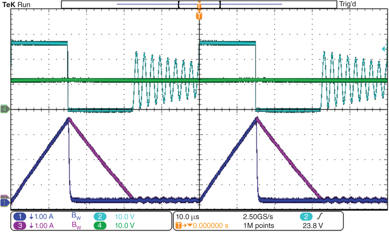
FIGURE 3.51 Workbench hardware: (1) input current, (2) switch-node voltage, (3) inductor current, and (4) output voltage.
Similar to the practical buck converter, the switch-node voltage of the practical buck-boost converter also rings, during ![]() with a peak-to-peak magnitude which is double that of the magnitude of the output voltage, clamped between 0 and Vin
+ Vo
:
with a peak-to-peak magnitude which is double that of the magnitude of the output voltage, clamped between 0 and Vin
+ Vo
:![]() .
.
3.15.5 Average Representation in CCM and DCM for Dynamic Analysis
In the previous sections, all three DC-DC converters are analyzed in DCM in steady state. Unlike the CCM, where the output voltage is dictated only by the input voltage ![]() and the transistor duty ratio, the output voltage in DCM also depends on the converter parameters and the operating condition. The output voltage at the voltage port of the switching power-pole is higher than that in the CCM case.
and the transistor duty ratio, the output voltage in DCM also depends on the converter parameters and the operating condition. The output voltage at the voltage port of the switching power-pole is higher than that in the CCM case.
If the duty ratio varies slowly, with a frequency an order of magnitude smaller than the switching frequency, then the average representation obtained on the basis of the DC steady state can be used for dynamic modeling in CCM and DCM by replacing uppercase letters with lowercase letters with an overbar (a “–” on top) to represent average quantities that are shown explicitly to be functions of time:
Therefore, as derived in the Appendix, in DCM, the average model of a switching power-pole in CCM by an ideal transformer is augmented by a dependent voltage source ![]() at the current port and by a dependent current source
at the current port and by a dependent current source ![]() at the voltage port, as shown in Figure 3.52a for buck and buck-boost converters and in Figure 3.52b for boost converters. The values of these dependent sources for the three converters are calculated in the Appendix, and only the results are presented in Table 3.2.
at the voltage port, as shown in Figure 3.52a for buck and buck-boost converters and in Figure 3.52b for boost converters. The values of these dependent sources for the three converters are calculated in the Appendix, and only the results are presented in Table 3.2.
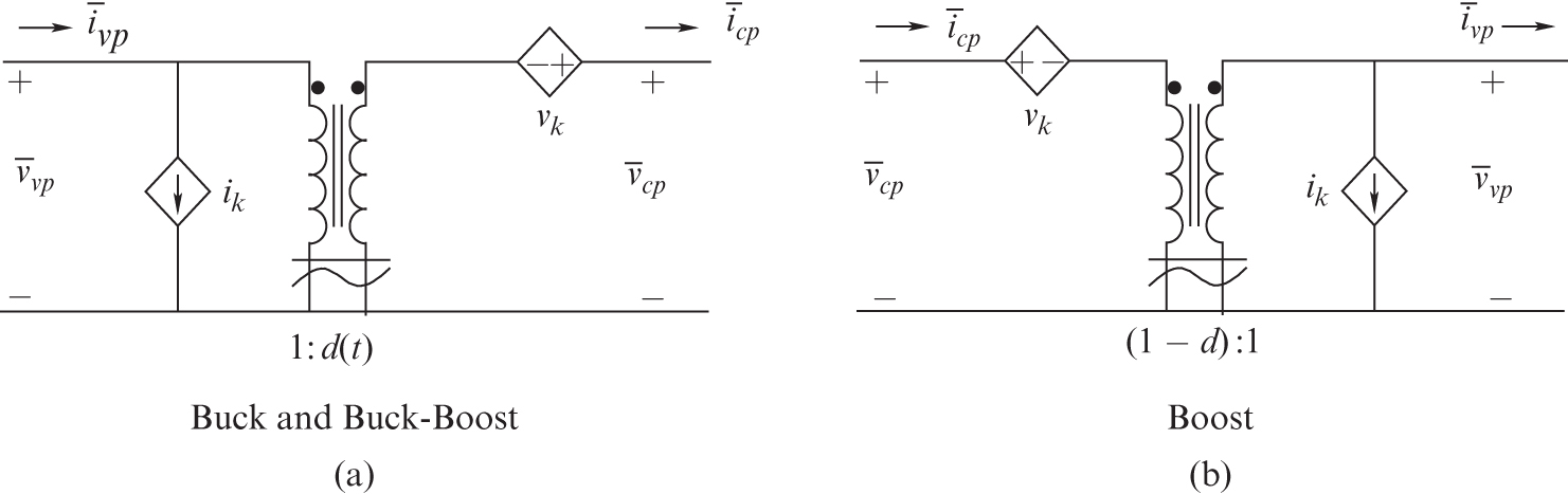
FIGURE 3.52 Average representation of a switching power-pole valid in CCM and DCM.
TABLE 3.2 Vk and Ik .
| Converter |
|
|
|---|---|---|
| Buck | ||
| Boost | ||
| Buck-Boost | ||
If ![]() and
and ![]() are expressed conditionally such that they are both zero in CCM and are expressed by the expressions in Table 3.2 only in DCM when the average inductor current falls below its critical value, then the representations in Figure 3.52 become valid for both the CCM and the DCM. In LTspice the ideal transformer itself is represented by a dependent current source and a dependent voltage source. The conditional dependent sources
are expressed conditionally such that they are both zero in CCM and are expressed by the expressions in Table 3.2 only in DCM when the average inductor current falls below its critical value, then the representations in Figure 3.52 become valid for both the CCM and the DCM. In LTspice the ideal transformer itself is represented by a dependent current source and a dependent voltage source. The conditional dependent sources ![]() and
and ![]() shown in Figures 3.52a and 3.52b are in addition to those used to represent the ideal transformer.
shown in Figures 3.52a and 3.52b are in addition to those used to represent the ideal transformer.
REFERENCES
- 1. N. Mohan, T.M. Undeland, and W.P. Robbins, Power Electronics: Converters, Applications and Design, 3rd Edition (New York: John Wiley & Sons, 2003).
- 2. Buck Converter Lab Manual. https://sciamble.com/resources/pe-drives-lab/basic-pe/buck-converter.
- 3. Boost Converter Lab Manual. https://sciamble.com/resources/pe-drives-lab/basic-pe/boost-converter.
- 4. Buck-Boost Converter Lab Manual. https://sciamble.com/resources/pe-drives-lab/basic-pe/ buck-boost-converter.
- 5. B. Carsten, “Converter Component Load Factors: A Performance Limitation of Various Topologies,” PCI Proceedings, June 1988, pp. 31–49.
- 6. M. Walters, “An Integrated Synchronous-Rectifier Power IC with Complementary-Switching (HIP5010, HIP5011),” Technical Brief, July 1995, TB332, Intersil Corp.
- 7. Synchronous-Rectified Buck Converter Lab Manual. https://sciamble.com/resources/pe-drives-lab/basic-pe/synchronous-buck-converter.
- 8. “Does GaN Have a Body Diode?—Understanding the Third Quadrant Operation of GaN,” Texas Instruments Application Report SNOAA36–February 2019. https://www.ti.com/lit/an/snoaa36/snoaa36.pdf?ts=1654535176366.
- 9. Buck Converter Discontinuous Conduction Mode Lab Manual. https://sciamble.com/resources/pe-drives-lab/basic-pe/buck-converter-dcm.
- 10. Boost Converter Discontinuous Conduction Mode Lab Manual. https://sciamble.com/resources/pe-drives-lab/basic-pe/boost-converter-dcm.
- 11. Buck-Boost Converter Discontinuous Conduction Mode Lab Manual. https://sciamble.com/resources/pe-drives-lab/basic-pe/buck-boost-converter-dcm.
PROBLEMS
Buck DC-DC Converters
Problems 3.1 through 3.6: In a buck DC-DC converter, ![]() . It is operating in DC steady state under the following conditions:
. It is operating in DC steady state under the following conditions:![]() ,
, ![]() ,
, ![]() , and
, and ![]() . Assume ideal components.
. Assume ideal components.
- 3.1 Calculate and draw the waveforms as shown in Figure 3.5d.
- 3.2 Draw the inductor voltage and current waveforms if
 ; all else is unchanged. Compare the ripple in the inductor current with that in Problem 3.1.
 - 3.3 In this buck converter, the output load is changing. Calculate the critical value of the output load
 below which the converter will enter the discontinuous conduction mode of operation.
 - 3.4 Calculate the critical value of the inductance
 such that this buck converter remains in the continuous conduction mode at and above
  under all values of the input voltage
  in a range from 24 V to 50 V.
 - 3.5 Draw the waveforms for the variables shown in Figure 3.5d for this buck converter at the output load that causes it to operate at the border of continuous and discontinuous modes.
- 3.6 In this buck converter, the input voltage is varying in a range from 24 V to 50 V. For each input value, the duty ratio is adjusted to keep the output voltage constant at its nominal value (with
 and
and  ). Calculate the minimum value of the inductance
  that will keep the converter in the continuous conduction mode at
  .
. - 3.7 A buck DC-DC converter is to be designed for
 ,
,  , and the maximum output power
  . The switching frequency is selected to be
  . Assume ideal components. Estimate the value of the filter inductance that should be used if the converter is to remain in CCM at one-third the maximum output power.
Boost DC-DC Converters
Problems 3.8 through 3.13: In a boost converter, ![]() . It is operating in DC steady state under the following conditions:
. It is operating in DC steady state under the following conditions: ![]() ,
, ![]() ,
, ![]() , and
, and ![]() . Assume ideal components.
. Assume ideal components.
- 3.8 Calculate and draw the waveforms as shown in Figure 3.12c.
- 3.9 Draw the inductor voltage and current waveforms, if
 ; all else is unchanged. Compare the ripple in the inductor current with that in Problem 3.8.
 - 3.10 In this boost converter, the output load is changing. Calculate the critical value of the output load
 below which the converter will enter the discontinuous conduction mode of operation.
 - 3.11 Calculate the critical value of the inductance
 below which this boost converter will enter the discontinuous conduction mode of operation at
  .
. - 3.12 Draw the waveforms for the variables in Figure 3.12c for this boost converter at the output load that causes it to operate at the border of continuous and discontinuous modes.
- 3.13 In this boost converter, the input voltage is varying in a range from 9 V to 15 V. For each input value, the duty ratio is adjusted to keep the output voltage constant at its nominal value (with
 and
and  ). Calculate the critical value of the inductance
  such that this boost converter remains in the continuous conduction mode at and above
  under all values of the input voltage
  .
. - 3.14 A boost converter is to be designed with the following values:
 ,
,  , and the maximum output power
  . The switching frequency is selected to be
  . Assume ideal components. Estimate the value of
  if the converter is to remain in CCM at one-third the maximum output power.
Boost DC-DC Converters
Problems 3.15 through 3.20: In a buck-boost converter, ![]() . It is operating in DC steady state under the following conditions:
. It is operating in DC steady state under the following conditions: ![]() ,
, ![]() ,
, ![]() , and
, and ![]() . Assume ideal components.
. Assume ideal components.
- 3.15 Calculate and draw the waveforms as shown in Figure 3.20c.
- 3.16 Draw the inductor voltage and current waveforms if
 ; all else is unchanged. Compare the ripple in the inductor current with that in Problem 3.15.
 - 3.17 In this buck-boost converter, the output load is changing. Calculate the critical value of the output load
 below which the converter will enter the discontinuous conduction mode of operation.
 - 3.18 Calculate the critical value of the inductance
 below which this buck-boost converter will enter the discontinuous conduction mode of operation at
- 3.19 Draw the waveforms for the variables in Figure 3.20c for this buck-boost converter at the output load that causes it to operate at the border of continuous and discontinuous modes.
- 3.20 In this buck-boost converter, the input voltage is varying in a range from 9 V to 15 V. For each input value, the duty ratio is adjusted to keep the output voltage constant at its nominal value (with
 and
and  ). Calculate the critical value of the inductance
  such that this buck-boost converter remains in the continuous conduction mode at and above
  under all values of the input voltage
  .
. - 3.21 A buck-boost converter is to be designed under the following conditions:
 ,
,  , and the maximum output power is
  . The switching frequency is selected to be
  . Assume ideal components. Estimate the value of
  if the converter is to remain in CCM at one-third the maximum output power.
SEPIC DC-DC Converters
- 3.22 In a SEPIC converter, assume the ripple in the inductor currents and the capacitor voltage to be zero. This SEPIC converter is operating in a DC steady state under the following conditions:
 ,
,  ,
,  , and
, and  . Assume ideal components. Draw the waveforms for all the converter variables under this DC steady-state condition.
 - 3.23 Show that the SEPIC converter consists of a switching power-pole as its building block.
Ćuk DC-DC Converters
- 3.24 In a Ćuk converter, assume the ripple in the inductor currents and the capacitor voltage to be zero. This Ćuk converter is operating in a DC steady state under the following conditions:
 ,
,  ,
,  , and
, and  . Assume ideal components. Draw the waveforms for all the converter variables under this DC steady-state condition.
 - 3.25 Show that the Ćuk converter consists of a switching power-pole as its building block.
Interleaving of DC-DC Converters
- 3.26 Two interleaved buck converters, each similar to the buck converter for Problem 3.1, are supplying a total of
 . Calculate and draw the waveforms of the total input current and the total current
  to the output stage. The gate signals to the converters are phase shifted by
  .
.
Regulation by PWM
- 3.27 In a buck converter, consider two values of duty ratios: 0.3 and 0.4. The switching frequency
 is 200 kHz and
  . Draw the waveforms as in Figure 3.36b.
Dynamic Average Models in CCM
- 3.28 Draw the dynamic average representations for buck, boost, buck-boost, SEPIC, and Ćuk converters in the continuous conduction mode for representation in LTspice.
- 3.29 In the converters based on average representations in Problem 3.28, calculate the average input current for each converter in terms of the average output current and the duty ratio
 .
.
Bi-Directional Switching Power-Poles
- 3.30 The DC-DC bi-directional converter shown in Figure 3.40a interfaces a 12/14-V battery with a 36/42-V battery bank. The internal emfs are
 (DC) and
  (DC). Both these battery sources have an internal resistance of
  each. In the DC steady state, calculate the power pole duty ratio
  if (a) the power into the low-voltage battery terminals is 140 W, and (b) the power out of the low-voltage battery terminals is 140 W.
DC-DC Converters in DCM
- 3.31 Derive the expressions for the critical resistance for the three converters given in Equation (3.45).
- 3.32 Derive the voltage ratio in DCM for a buck converter, given by Equation (3.48).
- 3.33 Derive the voltage ratio in DCM for a boost converter, given by Equation (3.53).
- 3.34 Derive the voltage ratio in DCM for a buck-boost converter, given by Equation (3.57).
- 3.35 Repeat the buck converter Problem 3.1 if
 is not specified but the load resistance is twice its critical value.
 - 3.36 Repeat the boost converter Problem 3.8 if
 is not specified but the load resistance is twice its critical value.
 - 3.37 Repeat the buck-boost converter Problem 3.15 if
 is not specified, but the load resistance is twice its critical value.
Sustainability-Related Questions
- 3.38 A 1.2 kW PV system consists of 4 series-connected arrays, each of which has a rated voltage of 55 V and a rated current of 6.0 A at the maximum power point, at the maximum expected insolation. The output of the series-connected arrays is boosted to 400 V (DC) by a boost converter as an input to an inverter that feeds power into the single-phase utility grid. Assuming that the switching frequency in the boost converter is selected to be 200 kHz and the peak-to-peak ripple in the input current to this converter is to be less than 10% of the rated current at the maximum power, calculate the value of the inductance in this converter. Assume ideal components.
- 3.39 In a large battery-storage system, the rated output voltage of a battery string is 650 V (DC), and the rated current is 1,200 A. The voltage can vary in a range from 500 V to 800 V. This output voltage is boosted to 900 V (DC), as an input to an inverter that interfaces with the three-phase utility grid. A switching power-pole with a bi-directional power capability is used. The switching frequency is selected to be 50 kHz, and the inductor value is selected such that the peak-to-peak ripple in the inductor current is less than 10% of the rated battery current, with the battery voltage at its rated value.
- Calculate the inductance value.
- Calculate the peak-to-peak ripple in the inductor current if operating at the rated current, but the battery voltage is at its minimum.
- Repeat part (b) if the battery voltage is at its maximum.
Simulation Problems
- 3.40 In the buck converter shown in Figure 3.5a, various parameters are as follows:
 . The input voltage
  , the switching frequency
  , and the switch duty ratio
  .
.- Plot the waveforms, after reaching the steady state, during the last 10 switching cycles for
 ,
,  , and
, and  .
. - Plot the average value of
 .
. - Plot
 and measure the peak-peak ripple
  and compare it with Equation (3.13).
 - Plot the
 waveform. What is the average of
  ? Compare the
  waveform with the ripple in
  .
. - Plot the input current waveform and calculate its average. Compare it to the value calculated from Equation (3.16).
- Plot the waveforms, after reaching the steady state, during the last 10 switching cycles for
- 3.41 In Problem 3.40, calculate the inductance value of
 , if
, if  should be
  of the load current. Verify the results by simulations.
 - 3.42 In Problem 3.40, change the output power to one-half its original value. Measure the peak-peak ripple
 and compare it with that in Problem 3.40c. Comment on this comparison.
 - 3.43 In the circuit of Problem 3.40, calculate
 from Equation (3.45) and verify by simulation whether the converter is operating on the boundary of CCM and DCM.
 - 3.44 In the boost converter shown in Figure 3.11, various parameters are as follows:
 . The input voltage
  , the switching frequency
  , and the switch duty ratio
  .
.- Plot the waveforms during the last 10 switching cycles, after reaching the steady state, for
 ,
,  , and
, and  .
. - Plot the average value of
 .
. - Plot
 and measure the peak-peak ripple
  and compare it with Equation (3.21).
 - Plot the
 and
and  waveform. What is the average of
  ? Compare the
  waveform with the ripple in
  .
. - Plot the input current waveform and calculate its average. Compare it to the value calculated from Equation (3.23).
- Plot the waveforms during the last 10 switching cycles, after reaching the steady state, for
- 3.45 In Problem 3.44, calculate the inductance value of
 , if
, if  should be
  of the input current. Verify the results by simulations.
 - 3.46 In Problem 3.44, change the output power to one-half its original value. Measure the peak-peak ripple
 and compare it with that in Problem 3.44c. Comment on this comparison.
 - 3.47 In Problem 3.44, calculate
 from Equation (3.45) and verify whether the converter is operating on the boundary of CCM and DCM.
 - 3.48 In the buck-boost converter shown in Figure 3.11, various parameters are as follows:
 . The input voltage
  , the switching frequency
  , and the switch duty ratio
  .
.- Plot the waveforms during the last 10 switching cycles, after reaching the steady state, for
 ,
,  and
and  .
. - Plot the average value of
 .
. - Plot
 and measure the peak-peak ripple
  and compare it with Equation (3.28).
 - Plot the
 and
and  waveform. What is the average of
  ? Compare the
  waveform with the ripple in
  .
. - Plot the input current waveform and calculate its average. Compare it to the value calculated from Equation (3.31).
- Plot the waveforms during the last 10 switching cycles, after reaching the steady state, for
- 3.49 In Problem 3.48, calculate the inductance value of
 , if
, if  should be
  of the input current. Verify the results by simulations.
 - 3.50 In Problem 3.48, change the output power to one-half its original value. Measure the peak-peak ripple
 and compare it with that in Problem 3.48c. Comment on this comparison.
 - 3.51 In Problem 3.48, calculate
 from Equation (3.45) and verify whether the converter is operating on the boundary of CCM and DCM.
 - 3.52 The buck-boost converter of Problem 3.48 is initially operating with an output load resistance
 . After the steady state is reached, an additional resistance of
  is switched in. Simulate this converter by representing the switching power-pole by its average model and compare the waveform of the inductor current in the average representation to that in switching representation.
 - 3.53 The buck-boost converter in Problem 3.48 is initially operating in DCM with
 .
.- Plot the waveforms during the last 5 switching cycles for
 ,
,  , and
, and  .
. - Plot the average value of
 .
. - Calculate
 using Equation (3.57) and compare it with its measured value.
 - Plot the waveform of
 , label it in terms of
  and
and  , and compare it with Figure 3.49a.
 - Show that the hatched area in Figure 3.49a, averaged over the switching time period, results in the increase in
 , compared to its CCM value.
- Plot the waveforms during the last 5 switching cycles for
APPENDIX 3A AVERAGE REPRESENTATION IN DISCONTINUOUS-CONDUCTION MODE (DCM)
3A.1 Introduction
Single-switch converters such as buck, boost, and buck-boost DC converters enter the discontinuous-conduction mode (DCM) under light-load conditions. In DCM, the inductor current becomes zero for a finite interval during a switching cycle. In the continuous-conduction mode (CCM), the building-block switch has two positions, either up or down. In DCM, the switch has another position (in the middle), thus resulting in three circuit sub-states during a switching cycle.
The following analysis shows that the average representation of single-switch converters in DCM consists of an ideal transformer (similar to that in CCM), augmented by dependent voltage and current sources. Such a representation allows a smooth transition between continuous and discontinuous modes.
3A.2 Average Representation in Discontinuous-Conduction Mode
3A.2.1 Buck and Buck-Boost Converters
The basic building block, with the switch and the diode in the appropriate positions for the buck and the buck-boost converters, is shown in Figure 3A.1a. The currents ![]() and
and ![]() and the voltage
and the voltage ![]() are shown in Figure 3A.1b, where
are shown in Figure 3A.1b, where ![]() is the voltage at the second terminal of the inductor, as defined in Figure 3A.1a. The switch duty ratio, controlled by the PWM-IC, is defined as
is the voltage at the second terminal of the inductor, as defined in Figure 3A.1a. The switch duty ratio, controlled by the PWM-IC, is defined as ![]() . The inductor current flows through the diode during
. The inductor current flows through the diode during ![]() , and the inductor current remains zero during
, and the inductor current remains zero during ![]() .
.
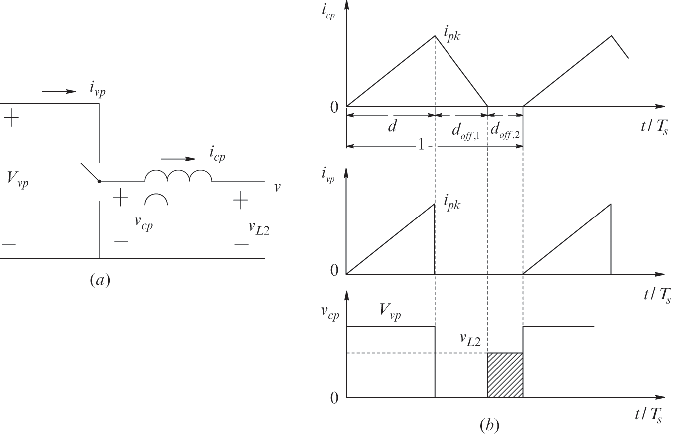
FIGURE 3A.1(a) Building Block. (b) Waveforms.
Based on voltages in the circuit of Figure 3A.1a, and the waveforms in Figure 3A.1b,
and
From Equations 3A.1 and 3A.2,
where
is a constant in terms of the inductance and the switching frequency ![]() .
.
The average equivalent circuit is shown in Figure 3.28a where the ideal transformer with the turns ratio ![]() is augmented by two dependent sources
is augmented by two dependent sources ![]() and
and ![]() . The expressions for these dependent sources can be calculated easily, as shown below:
. The expressions for these dependent sources can be calculated easily, as shown below:
In the model of Figure 3.52a,
From the waveforms in Figure 3A.1b,
Substituting for ![]() from Equation 3A.6, and for
from Equation 3A.6, and for ![]() from Equation 3A.3 into Equation 3A.5,
from Equation 3A.3 into Equation 3A.5,
To calculate ![]() in Figure 3.28a, the average of the voltage at the current port is
in Figure 3.28a, the average of the voltage at the current port is
From Figure 3A.2,
Substituting Equation 3A.8 and Equation 3A.3 into Equation 3A.9,
At the transition from the DCM to CCM, both ![]() and
and ![]() must go to zero simultaneously in the model of Figure 3.52a. The critical value of the current at the boundary of DCM and CCM, from either Equation 3A.7 for
must go to zero simultaneously in the model of Figure 3.52a. The critical value of the current at the boundary of DCM and CCM, from either Equation 3A.7 for ![]() or Equation 3A.10 for
or Equation 3A.10 for ![]() is
is
3A.2.1.1 Expressions for Buck Converters
The above analysis was general, applicable to buck as well as buck-boost converters. Specifically in buck converters, ![]() ,
, ![]() , and
, and ![]() . Therefore,
. Therefore,
and
3A.2.1.2 Expressions for Buck-Boost Converters
In buck-boost converters, ![]() ,
, ![]() , and
, and ![]() . Therefore,
. Therefore,
and
3A.2.2 Boost Converters
The average representation for boost converters operating in DCM is shown in Figure 3.52b. A similar analysis as for buck and buck-boost converters results in the following equations:
and
3A.3 Average Modeling in PSpice for Large Signal Disturbances
To keep it general so that the models in PSpice are valid both in CCM and DCM, the dependent sources in Figure 3.52a and Figure 3.52b should be represented by conditional expressions, which make them go to zero in CCM.