
8
SWITCH-MODE DC POWER SUPPLIES
8.1 APPLICATIONS OF SWITCH-MODE DC POWER SUPPLIES
Switch-mode DC power supplies represent an important power electronics application area with a worldwide market of several billion dollars per year. Many of these power supplies incorporate transformer isolation for reasons that are discussed below. Within these power supplies, transformer-isolated DC-DC converters are derived from non-isolated DC-DC converter topologies already discussed in Chapter 3. For short, we will refer to transformer-isolated switch-mode DC power supplies as SMPS (switched-mode power supply, sometimes called switcher), whose block diagram is shown in Figure 8.1. As shown in Figure 8.1, these supplies encompass the rectification of the utility supply, and the voltage ![]() across a large filter capacitor is the input to the transformer-isolated DC-DC converter, which is the focus of discussion in this chapter. Internally, the transformer operates at very high frequencies, typically upwards of a few hundred kHz, thus resulting in small size and weight, as discussed in the next chapter.
across a large filter capacitor is the input to the transformer-isolated DC-DC converter, which is the focus of discussion in this chapter. Internally, the transformer operates at very high frequencies, typically upwards of a few hundred kHz, thus resulting in small size and weight, as discussed in the next chapter.

FIGURE 8.1 Block diagram of switch-mode DC power supplies.
8.2 NEED FOR ELECTRICAL ISOLATION
Electrical isolation by means of transformers is needed in switch-mode DC power supplies for three reasons:
- Safety: It is necessary for the low-voltage DC output to be isolated from the utility supply to avoid the shock hazard.
- Different reference potentials: The DC supply may have to operate at a different potential, for example, the DC supply to the gate drive for the upper MOSFET in the power pole is referenced to its source.
- Voltage matching: If the DC-DC conversion is large, then to avoid requiring large voltage and current ratings of semiconductor devices, it may be economical and operationally more suitable to use an electrical transformer for conversion of voltage levels.
8.3 CLASSIFICATION OF TRANSFORMER-ISOLATED DC-DC CONVERTERS
In the block diagram of Figure 8.1, there are the following three categories of transformer-isolated DC-DC converters, all of which are discussed in detail in this chapter:
- Flyback converters derived from buck-boost DC-DC converters
- Forward converter derived from buck DC-DC converters
- Full-bridge and half-bridge converters derived from buck DC-DC converters
8.4 FLYBACK CONVERTERS
Flyback converters are very commonly used in applications at low power levels below 50 W. These are derived from the buck-boost converter redrawn in Figure 8.2a, where the inductor is drawn descriptively on a low permeability core.

FIGURE 8.2 Buck-boost and the flyback converters.
The flyback converter in Figure 8.2b consists of two mutually coupled coils, where the coil orientations are such that at the instant when the transistor is turned off, the current switches to the second coil to maintain the same flux in the core. Therefore, the dots on coils are as shown in Figure 8.2b, where the current into the dot of either coil produces core flux in the same direction. Commonly, the circuit of Figure 8.2b is redrawn as in Figure 8.2c.
We will consider the steady state in the incomplete demagnetization mode, where the energy is never completely depleted from the magnetic core. This corresponds to the continuous conduction mode (CCM) in buck-boost converters. We will assume ideal devices and components, the output voltage ![]() , and the leakage inductances to be zero.
, and the leakage inductances to be zero.
Turning on the transistor at ![]() in the circuit in Figure 8.2c applies the input voltage
in the circuit in Figure 8.2c applies the input voltage ![]() across coil 1, and the core magnetizing flux
across coil 1, and the core magnetizing flux ![]() increases linearly from its initial value
increases linearly from its initial value ![]() , as shown in the waveforms of Figure 8.3. During the transistor on interval
, as shown in the waveforms of Figure 8.3. During the transistor on interval ![]() , the increase in flux can be calculated from Faraday’s law as:
, the increase in flux can be calculated from Faraday’s law as:

FIGURE 8.3 Flyback converter waveforms.
Due to increasing ![]() , the induced voltage
, the induced voltage ![]() across coil 2 adds to the output voltage
across coil 2 adds to the output voltage ![]() to reverse bias the diode, resulting in
to reverse bias the diode, resulting in ![]() . Corresponding to the core flux, the current
. Corresponding to the core flux, the current ![]() can be calculated using the relationship
can be calculated using the relationship ![]() , where
, where ![]() is the core reluctance in the flux path. Therefore, using Equation (8.1), the increase in the input current during the on interval from its initial value
is the core reluctance in the flux path. Therefore, using Equation (8.1), the increase in the input current during the on interval from its initial value ![]() can be calculated as
can be calculated as
During the on interval ![]() , the output load is entirely supplied by the energy stored in the output capacitor, and the core magnetizing flux and the input current reach their peak values at the end of this interval:
, the output load is entirely supplied by the energy stored in the output capacitor, and the core magnetizing flux and the input current reach their peak values at the end of this interval:
where ![]() is the magnetizing inductance of the transformer seen from the primary side. After the on interval, turning off the transistor forces the input current in Figure 8.2c to zero. The magnetic energy stored in the magnetic core due to the flux
is the magnetizing inductance of the transformer seen from the primary side. After the on interval, turning off the transistor forces the input current in Figure 8.2c to zero. The magnetic energy stored in the magnetic core due to the flux ![]() cannot change instantaneously, and hence the ampere-turns applied to the core must be the same at the instant immediately before and after turning the transistor off. Therefore, the current
cannot change instantaneously, and hence the ampere-turns applied to the core must be the same at the instant immediately before and after turning the transistor off. Therefore, the current ![]() in coil 2 through the diode suddenly jumps to its peak value such that
in coil 2 through the diode suddenly jumps to its peak value such that
With the diode conducting, the output voltage ![]() appears across coil 2 with a negative polarity. Hence, during the off interval
appears across coil 2 with a negative polarity. Hence, during the off interval ![]() , the core flux declines linearly, as plotted in Figure 8.3, by
, the core flux declines linearly, as plotted in Figure 8.3, by ![]() , where
, where
Using Equations (8.1) and (8.7),
The change in the current ![]() can be calculated in a manner similar to Equation (8.2), and this current is plotted in Figure 8.3.
can be calculated in a manner similar to Equation (8.2), and this current is plotted in Figure 8.3.
Equation (8.8) shows that in a flyback converter, the dependence of the voltage ratio on the duty ratio ![]() is identical to that in the buck-boost converter, and it also depends on the coils’ turns ratio
is identical to that in the buck-boost converter, and it also depends on the coils’ turns ratio ![]() Flyback converters require the minimum number of components by integrating the inductor (needed for a buck-boost operation) with the transformer that provides electrical isolation and matching of the voltage levels. These converters are very commonly used in low-power applications in the complete demagnetization mode (corresponding to the discontinuous conduction mode in buck-boost), which makes their control easier. A disadvantage of flyback converters is the need for snubbers to prevent voltage spikes across the transistor and diode due to leakage inductances associated with the two coils
Flyback converters require the minimum number of components by integrating the inductor (needed for a buck-boost operation) with the transformer that provides electrical isolation and matching of the voltage levels. These converters are very commonly used in low-power applications in the complete demagnetization mode (corresponding to the discontinuous conduction mode in buck-boost), which makes their control easier. A disadvantage of flyback converters is the need for snubbers to prevent voltage spikes across the transistor and diode due to leakage inductances associated with the two coils
Example 8.1
In a flyback converter, shown in Figure 8.2c, ![]() ,
, ![]() ,
, ![]() , and the magnetizing inductance
, and the magnetizing inductance ![]() . This converter is operating in equivalent CCM with a switching frequency
. This converter is operating in equivalent CCM with a switching frequency ![]() and supplying an output load
and supplying an output load ![]() . Assuming this converter to be lossless, calculate the waveforms associated with it.
. Assuming this converter to be lossless, calculate the waveforms associated with it.
Solution
From Equation (8.8), the duty ratio ![]() , where
, where ![]() . The average currents are
. The average currents are ![]() and
and ![]() . In Figure 8.3, the rise in current during the on interval
. In Figure 8.3, the rise in current during the on interval ![]() can be calculated as
can be calculated as
From the waveforms of Figure 8.3, the average input current can be calculated as follows:
From the equations above, in Figure 8.3, ![]() and
and ![]() . The output current has a peak value
. The output current has a peak value ![]() and
and ![]() .
.
8.4.1 Simulation and Hardware Prototyping—CCM without Snubber
The simulation of a nonideal flyback converter is demonstrated by means of an example:
Example 8.2
In the flyback converter shown in Figure 8.2c, ![]() , and
, and ![]() . It is operating in DC steady state under the following conditions:
. It is operating in DC steady state under the following conditions: ![]() ,
, ![]() , and
, and ![]() . The transformer’s primary-to-secondary turns ratio is 2:1. The primary side has a magnetizing inductance of
. The transformer’s primary-to-secondary turns ratio is 2:1. The primary side has a magnetizing inductance of ![]() and a leakage inductance of
and a leakage inductance of ![]() . For the switch and the diode, use the parameters given in the Appendix of Chapter 2. Simulate this converter using LTspice.
. For the switch and the diode, use the parameters given in the Appendix of Chapter 2. Simulate this converter using LTspice.
Solution The simulation file used in this example is available on the accompanying website. The LTspice model is as shown in Figure 8.4, and the steady-state waveforms from the simulation of this model are shown in Figure 8.5.

FIGURE 8.4 LTspice model.

FIGURE 8.5 LTspice simulation results.
The Workbench model for implementing the above example in hardware using the Sciamble lab kit is as shown in Figure 8.6.

FIGURE 8.6 Workbench model.
The steady-state waveforms from running the flyback converter using the Sciamble laboratory kit are shown in Figure 8.7. The step-by-step procedure for re-creating the above hardware implementation is presented in [1].

FIGURE 8.7 Workbench hardware results: (1) Input current, (2) Switch-node voltage, (3) Diode current and (4) Output voltage.
8.4.2 RCD Snubber
Unlike the case of an ideal flyback converter waveform shown in Figure 8.3, the switch-node voltage waveform of a practical flyback converter, shown in Figure 8.8, has significant ringing. The energy stored in the leakage inductance ![]() , unlike the energy stored in the magnetizing inductance
, unlike the energy stored in the magnetizing inductance ![]() , does not transfer over to the secondary side when the switch is turned off. This energy charges up the switch’s parasitic capacitance, leading to a high voltage across the switch, causing significant voltage stress, which can damage the switch, the transformer insulation, or both.
, does not transfer over to the secondary side when the switch is turned off. This energy charges up the switch’s parasitic capacitance, leading to a high voltage across the switch, causing significant voltage stress, which can damage the switch, the transformer insulation, or both.
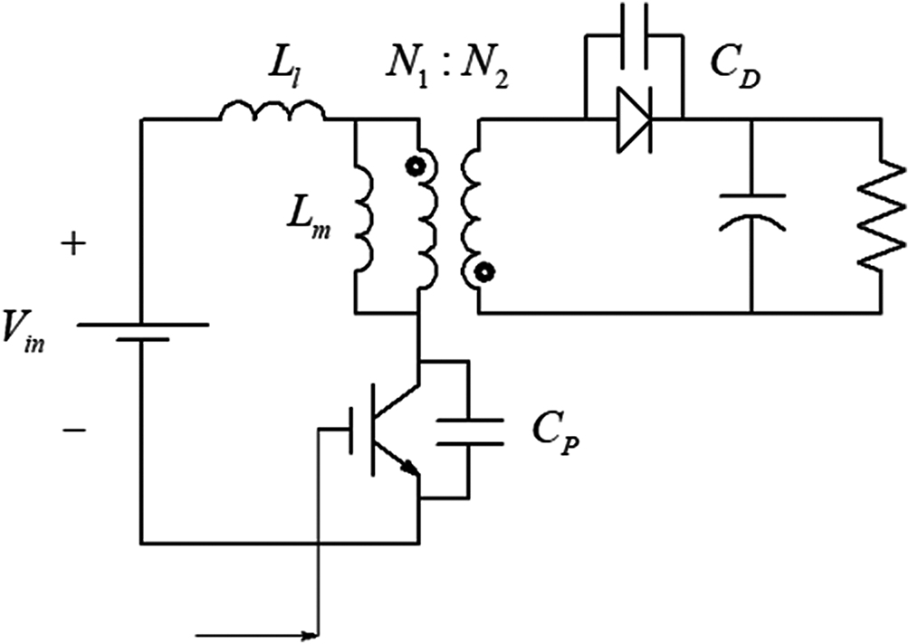
FIGURE 8.8 Practical flyback converter parasitic elements.
In a practical flyback converter, the magnitude of the voltage swing is clamped by the use of a snubber circuit [2]. This section presents the operation and design of one of the commonly used snubber circuit, RCD snubber, shown in Figure 8.9.

FIGURE 8.9 RCD snubber.
We will first analyze the steady-state operation of the snubber circuit before proceeding with how to determine the snubber parameters. The voltage across the snubber capacitor is assumed to be a constant ![]() , which is justified given a sufficiently large
, which is justified given a sufficiently large ![]() .
.
8.4.2.1 Steady-State Operation of RCD Snubber
At time ![]() , when the transistor is on, as shown in Figure 8.10a, the primary current increases linearly, as shown in Figure 8.10b. During this period, the voltage across the transistor is
, when the transistor is on, as shown in Figure 8.10a, the primary current increases linearly, as shown in Figure 8.10b. During this period, the voltage across the transistor is ![]() as shown in Figure 8.10c, and there is no current flowing into the snubber circuit because the diode
as shown in Figure 8.10c, and there is no current flowing into the snubber circuit because the diode ![]() is reverse biased with a voltage of
is reverse biased with a voltage of ![]() across it, as shown in Figure 8.10d. The snubber capacitor is slowly discharged by the snubber resistor, as shown by the negative current,
across it, as shown in Figure 8.10d. The snubber capacitor is slowly discharged by the snubber resistor, as shown by the negative current, ![]() in Figure 8.10e.
in Figure 8.10e.

FIGURE 8.10 RCD snubber waveforms
When the transistor is turned off, the parasitic capacitance ![]() is charged up to the sum of the input voltage and the reflected secondary voltage,
is charged up to the sum of the input voltage and the reflected secondary voltage, ![]() where
where ![]() . During this interval,
. During this interval, ![]() , the energy stored in the magnetizing inductance contributes to a very rapid charging of the transistor’s parasitic capacitance
, the energy stored in the magnetizing inductance contributes to a very rapid charging of the transistor’s parasitic capacitance ![]() as well as the discharging of the secondary side diode’s junction capacitance
as well as the discharging of the secondary side diode’s junction capacitance ![]() . The input current
. The input current ![]() remains relatively constant, given the negligible energy transfer from the magnetizing inductance to the parasitic capacitances.
remains relatively constant, given the negligible energy transfer from the magnetizing inductance to the parasitic capacitances.
Once the secondary side diode’s junction capacitance is fully discharged, and the diode begins conducting and simultaneously ![]() is charged to
is charged to ![]() , the energy stored in the magnetizing inductance starts charging the output capacitor.
, the energy stored in the magnetizing inductance starts charging the output capacitor.
During the time interval ![]() , the snubber diode is still reverse biased since
, the snubber diode is still reverse biased since ![]() . The voltage across the transistor continues to rise until it reaches
. The voltage across the transistor continues to rise until it reaches ![]() (plus the diode forward voltage drop, which is assumed to be negligible in this discussion), forward biasing the snubber diode. The primary current during this interval falls rapidly as only the energy stored in the primary side leakage inductance is available to charge
(plus the diode forward voltage drop, which is assumed to be negligible in this discussion), forward biasing the snubber diode. The primary current during this interval falls rapidly as only the energy stored in the primary side leakage inductance is available to charge ![]() .
.
In the absence of the snubber circuit, the energy in the leakage inductance continues to charge ![]() , which leads to high voltage ringing across the transistor, as seen in Figure 8.7. In addition to the issue of high voltage, the ringing frequency, given by Equation (8.9), is typically in the order of MHz and is a source of significant noise and EMI:
, which leads to high voltage ringing across the transistor, as seen in Figure 8.7. In addition to the issue of high voltage, the ringing frequency, given by Equation (8.9), is typically in the order of MHz and is a source of significant noise and EMI:
In the presence of the snubber circuit, the primary current flows through the forward-biased snubber diode, charging the snubber capacitor. ![]() remains relatively a constant by design, as explained in the next section. During this interval,
remains relatively a constant by design, as explained in the next section. During this interval, ![]() , the primary current continues to fall rapidly. The voltage across the transistor remains clamped at
, the primary current continues to fall rapidly. The voltage across the transistor remains clamped at ![]() .
.
Once the leakage energy is fully transferred to the clamp capacitor at time ![]() , the primary current goes to
, the primary current goes to ![]() , and the snubber diode gets reverse biased as the transistor voltage drops from
, and the snubber diode gets reverse biased as the transistor voltage drops from ![]() to
to ![]() .
.
Example 8.3
In Example 8.1, calculate the frequency of the ringing of the voltage across the transistor when it turns off. The transistor’s parasitic capacitance ![]() .
.
Solution From Equation (8.9), ![]() .
.
8.4.2.2 Design of RCD Snubber
At steady state, since the voltage across the snubber capacitor is a constant, the current through the capacitor averaged over a switching cycle ![]() is zero:
is zero:
During the time interval ![]() , when the snubber diode is forward biased, the voltage across the inductor from Figure 8.8 is the sum of the voltage across the snubber capacitor and the voltage across the transformer primary winding:
, when the snubber diode is forward biased, the voltage across the inductor from Figure 8.8 is the sum of the voltage across the snubber capacitor and the voltage across the transformer primary winding:
The current through the leakage inductor goes from approximately ![]() to zero, as seen in Figure 8.10b. The duration of the interval when the snubber diode is conducting can be obtained from Equation (8.11):
to zero, as seen in Figure 8.10b. The duration of the interval when the snubber diode is conducting can be obtained from Equation (8.11):
The expression for the snubber resistor can be obtained using Equations (8.10) and (8.12):
Given the converter operating condition and the desired maximum transistor voltage, the snubber resistor can be determined using the above expression. The lower the tolerable voltage across the transistor, the smaller the snubber resistor and thus higher losses in the snubber circuit. The power lost in the snubber circuit is:
where ![]() is the leakage inductor power, the energy stored in the leakage inductor per switching cycle time period.
is the leakage inductor power, the energy stored in the leakage inductor per switching cycle time period. ![]() is the factor by which the losses in the circuit are scaled due to the presence of the snubber compared to the circuit without a snubber. Since
is the factor by which the losses in the circuit are scaled due to the presence of the snubber compared to the circuit without a snubber. Since ![]() ,
, ![]() is always greater than 1. The higher the snubber voltage, the lower the losses and vice versa.
is always greater than 1. The higher the snubber voltage, the lower the losses and vice versa.
The value of the snubber capacitor isn’t as crucial as that of the resistor. The only requirement is that the capacitance is large enough to maintain the snubber voltage a constant. An approximate expression can be obtained from the snubber capacitor current waveform in Figure 8.10e. Assuming that the current in the snubber resistor is negligible compared to the peak input current ![]() , during the interval when the snubber diode is reverse biased:
, during the interval when the snubber diode is reverse biased:
In the above expression ![]() is the ratio of the snubber capacitor peak-peak ripple voltage and the snubber capacitor average voltage over a switching cycle. This value is typically chosen between 0.01 and 0.1.
is the ratio of the snubber capacitor peak-peak ripple voltage and the snubber capacitor average voltage over a switching cycle. This value is typically chosen between 0.01 and 0.1.
The diode must be a fast-acting diode such as the Schottky diode since the conduction period ![]() typically lasts for a short interval.
typically lasts for a short interval.
Design a snubber for the flyback converter in Example 8.1. Assume that the snubber diode is ideal and the peak input current is ![]() . The voltage across the transistor should not exceed
. The voltage across the transistor should not exceed ![]() under the given operating conditions.
under the given operating conditions.
Solution Using Equation (8.8), under ideal conditions.
The snubber capacitor voltage must be chosen such that it is greater than the voltage across the transistor when it is off and less than the given maximum allowable voltage across the transistor, i.e.,
allowing for a snubber capacitor ripple of ![]() , which is
, which is ![]() at the worst case. To keep within the specified snubber voltage limit, accounting for the ripple, the voltage is chosen to be
at the worst case. To keep within the specified snubber voltage limit, accounting for the ripple, the voltage is chosen to be ![]() .
.
The snubber resistance can be obtained using Equation (8.13):
The power lost in the snubber circuit can be obtained using Equation (8.14):
which is about 6 times the leakage inductance power ![]() , and is otherwise lost without the snubber circuit.
, and is otherwise lost without the snubber circuit.
The snubber capacitance is obtained using Equation (8.15):
8.4.3 Simulation and Hardware Prototyping—CCM with Snubber
The simulation of a nonideal flyback converter with a primary side snubber is demonstrated by means of an example:
In the flyback converter shown in Figure 8.2c, ![]() , and
, and ![]() . It is operating in DC steady state under the following conditions:
. It is operating in DC steady state under the following conditions: ![]() ,
, ![]() , and
, and ![]() . The transformer’s primary-to-secondary turns ratio is 2:1. The primary side has a magnetizing inductance of
. The transformer’s primary-to-secondary turns ratio is 2:1. The primary side has a magnetizing inductance of ![]() and a leakage inductance of
and a leakage inductance of ![]() . The snubber resistance
. The snubber resistance ![]() and the snubber capacitance
and the snubber capacitance ![]() . For the switch and the diode, use the parameters given in the Appendix of Chapter 2. Simulate this converter using LTspice.
. For the switch and the diode, use the parameters given in the Appendix of Chapter 2. Simulate this converter using LTspice.
Solution The simulation file used in this example is available on the accompanying website. The LTspice model is shown in Figure 8.11, and the steady-state waveforms from the simulation of this model are shown in Figure 8.12.

FIGURE 8.11 LTspice model.

FIGURE 8.12 LTspice simulation results.
The Workbench model for implementing the above example in hardware using the Sciamble lab kit is the same as the one shown in Figure 8.6. The steady-state waveforms from running the flyback converter with an RCD snubber using the Sciamble laboratory kit are shown in Figure 8.13. The step-by-step procedure for re-creating the above hardware implementation is presented in [3].

FIGURE 8.13 Workbench hardware results: (1) Input current, (2) Switch-node
As seen in Figure 8.13, the voltage across the switch is clamped to within the ![]() design requirement given in Example 8.4.
design requirement given in Example 8.4.
8.4.4 Simulation and Hardware Prototyping—DCM with Snubber
In the previous sections, the operation of the flyback converter was considered under continuous conduction mode. The operation of the flyback converter under discontinuous conduction mode is mostly similar to that of the buck-boost converter. The simulation of a nonideal flyback converter with a primary side snubber under discontinuous conduction mode is demonstrated by means of an example:
Example 8.6
The flyback converter in Example 8.5 is operating at a duty of ![]() and the load resistance
and the load resistance ![]() . Simulate this converter using LTspice.
. Simulate this converter using LTspice.
Solution The simulation file used in this example is available on the accompanying website. The LTspice model is the same as the one shown in Figure 8.11, and the steady-state waveforms from the simulation of this model are shown in Figure 8.14.

FIGURE 8.14 LTspice simulation results.
The Workbench model for implementing the above example in hardware using the Sciamble lab kit is the same as the one shown in Figure 8.6. The steady-state waveforms from running the flyback converter with an RCD snubber using the Sciamble laboratory kit under DCM are shown in Figure 8.15.

FIGURE 8.15 Workbench hardware results: (1) Input current, (2) Switch-node voltage, (3) Diode current and (4) Secondary side voltage.
Under DCM, when the secondary side current goes to zero, and the diode is reverse biased, the voltage across the transistor transitions from ![]() to
to ![]() . The frequency of this ringing is given by:
. The frequency of this ringing is given by:
Many commercially available flyback converter controller ICs, such as Texas Instruments’ UCC28704, typically operate under DCM to make use of the inherent ringing of the transistor voltage to turn on the transistor when the voltage across the switch is at the lowest point, thereby reducing the switching losses.
So far, we have only discussed the design of snubber for the primary side. As seen in Figure 8.15, there is significant ringing in the voltage across the secondary side due to the leakage inductance and the diode’s junction capacitance. The frequency of this typically tends to be much higher than that of the primary side ringing. This can be addressed by the use of a simple RC snubber across the diode, as presented in [2].
8.5 FORWARD CONVERTERS
The forward converter and its variations derived from a buck converter are commonly used in applications at low power levels up to 1 kW. A buck converter is shown in Figure 8.16a. In this circuit, a three-winding transformer is added, as shown in Figure 8.16b, to realize a forward converter. The third winding in series with a diode ![]() , and the diode
, and the diode ![]() are needed to demagnetize the core every switching cycle. The winding orientations in Figure 8.16b are such that the current into the dot of any of the windings will produce core flux in the same direction. We will consider steady-state converter operation in the continuous conduction mode where the output inductor current
are needed to demagnetize the core every switching cycle. The winding orientations in Figure 8.16b are such that the current into the dot of any of the windings will produce core flux in the same direction. We will consider steady-state converter operation in the continuous conduction mode where the output inductor current ![]() flows continuously. In the following analysis, we will assume ideal semiconductor devices,
flows continuously. In the following analysis, we will assume ideal semiconductor devices, ![]() , and the leakage inductances to be zero.
, and the leakage inductances to be zero.

FIGURE 8.16 Buck and forward converters.
Initially, assuming an ideal transformer in the forward converter of Figure 8.16b, the third winding and the diode ![]() can be removed, and
can be removed, and ![]() can be replaced by a short circuit. In such an ideal case, the forward converter operation is identical to that of the buck converter, as shown by the waveform in Figure 8.17, except for the presence of the transformer turns ratio
can be replaced by a short circuit. In such an ideal case, the forward converter operation is identical to that of the buck converter, as shown by the waveform in Figure 8.17, except for the presence of the transformer turns ratio ![]() . Therefore, in the continuous conduction mode,
. Therefore, in the continuous conduction mode,

FIGURE 8.17 Forward converter operation.
In the case of a real transformer, the core must be completely demagnetized during the off interval of the transistor, hence the need for the third winding and the diodes ![]() and
and ![]() , as shown in Figure 8.4b. Turning on the transistor causes the magnetizing flux in the core to build up, as shown in Figure 8.18. During this on-interval
, as shown in Figure 8.4b. Turning on the transistor causes the magnetizing flux in the core to build up, as shown in Figure 8.18. During this on-interval ![]() ,
, ![]() gets reverse biased, thus preventing the current from flowing through the tertiary winding. The diode
gets reverse biased, thus preventing the current from flowing through the tertiary winding. The diode ![]() also gets reverse biased, and the output inductor current flows through
also gets reverse biased, and the output inductor current flows through ![]() .
.

FIGURE 8.18 Forward converter core flux.
When the transistor is turned off, the magnetic energy stored in the transformer core forces a current to flow into the dotted terminal of the tertiary winding since the current into the dotted terminal of the secondary winding cannot flow due to ![]() , which results in
, which results in ![]() being applied negatively across the tertiary winding, and the core flux to decline, as shown in Figure 8.6. (The output inductor current freewheels through
being applied negatively across the tertiary winding, and the core flux to decline, as shown in Figure 8.6. (The output inductor current freewheels through ![]() .) After an interval
.) After an interval ![]() , the core flux comes to zero and stays zero during the remaining interval until the next cycle begins.
, the core flux comes to zero and stays zero during the remaining interval until the next cycle begins.
To avoid the core from saturating, ![]() must be less than the off interval
must be less than the off interval ![]() of the transistor. Typically, windings 1 and 3 are wound bifilar to provide a very tight mutual coupling between the two, and hence,
of the transistor. Typically, windings 1 and 3 are wound bifilar to provide a very tight mutual coupling between the two, and hence, ![]() . Therefore, a per-turn voltage of equal magnitude but opposite polarity is applied to the core during
. Therefore, a per-turn voltage of equal magnitude but opposite polarity is applied to the core during ![]() and
and ![]() . With
. With ![]() ,
, ![]() , and at the upper limit,
, and at the upper limit, ![]() and
and ![]() are both equal to
are both equal to ![]() . Therefore, with
. Therefore, with ![]() , the upper limit on the duty ratio is
, the upper limit on the duty ratio is ![]() .
.
In a forward converter, shown in Figure 8.16b, ![]() ,
, ![]() ,
, ![]() ,
, ![]() , and the magnetizing inductance
, and the magnetizing inductance ![]() . This converter is operating in equivalent CCM with a switching frequency
. This converter is operating in equivalent CCM with a switching frequency ![]() and supplying an output load
and supplying an output load ![]() . Assume the filter inductor current
. Assume the filter inductor current ![]() to be ripple-free. Assuming this converter to be lossless, calculate the waveforms associated with it.
to be ripple-free. Assuming this converter to be lossless, calculate the waveforms associated with it.
Solution From Equation (8.17), the duty ratio ![]() , where
, where ![]() . The average currents are
. The average currents are ![]() and
and ![]() . The voltage waveforms are shown in Figure 8.19, where the output current reflected to the primary side is
. The voltage waveforms are shown in Figure 8.19, where the output current reflected to the primary side is ![]() . The peak of the magnetizing current during the on interval
. The peak of the magnetizing current during the on interval ![]() can be calculated as
can be calculated as
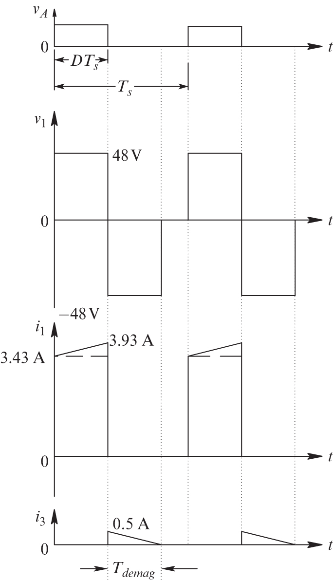
FIGURE 8.19 Waveforms in the forward converter of Example 8.7.
During the transistor off interval, this magnetizing current, flowing through the diode D3, decreases and comes to zero after ![]() , as shown in Figure 8.19.
, as shown in Figure 8.19.
8.5.1 Simulation and Hardware Prototyping
The simulation of a nonideal forward converter is demonstrated by means of an example:
Example 8.8
In the forward converter shown in Figure 8.16c, ![]() ,
, ![]() ,
, ![]() ,
, ![]() , and
, and ![]() . It is operating in DC steady state under the following conditions:
. It is operating in DC steady state under the following conditions: ![]() ,
, ![]() , and
, and ![]() . The primary side has a magnetizing inductance of
. The primary side has a magnetizing inductance of ![]() and a leakage inductance of
and a leakage inductance of ![]() . For the switch and the diode, use the parameters given in the Appendix of Chapter 2. Simulate this converter using LTspice.
. For the switch and the diode, use the parameters given in the Appendix of Chapter 2. Simulate this converter using LTspice.
Solution The simulation file used in this example is available on the accompanying website. The LTspice model is, as shown in Figure 8.20, and the steady-state waveforms from the simulation of this model are shown in Figure 8.21.

FIGURE 8.20 LTspice model.

FIGURE 8.21 LTspice simulation results.
The Workbench model for implementing the above example in hardware using the Sciamble lab kit is as shown in Figure 8.22.

FIGURE 8.22 Workbench model.
The steady-state waveforms from running the forward converter using the Sciamble laboratory kit are shown in Figure 8.23. The step-by-step procedure for re-creating the above hardware implementation is presented in [4].
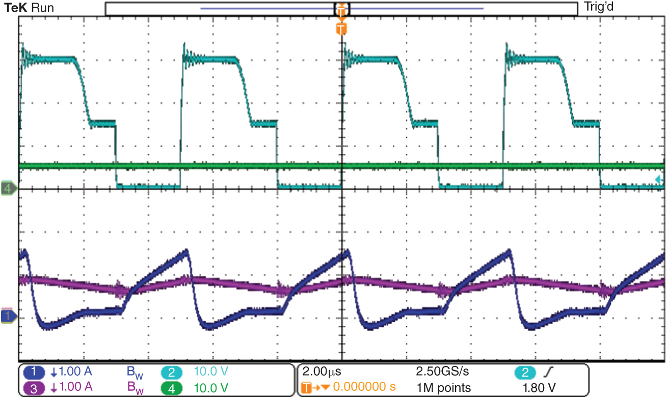
FIGURE 8.23 Workbench hardware results: (1) Input current, (2) Switch-node voltage, (3) Diode current and (4) Output voltage.
Unlike the voltage across the transistor of the flyback converter without a snubber, as seen in Figure 8.7, the voltage across the transistor of a forward converter without a snubber doesn’t ring as much as seen in Figure 8.23. This is due to two reasons: the forward converter transformer typically has lower leakage inductance due to tighter coupling between the primary and the demagnetization winding, and sustained voltage greater than ![]() across the transistor will lead to forward-biasing the demagnetization winding diode, thus effectively clamping the voltage at the sum of
across the transistor will lead to forward-biasing the demagnetization winding diode, thus effectively clamping the voltage at the sum of ![]() and the diode forward voltage drop.
and the diode forward voltage drop.
In cases where the leakage inductance of the transformer is high or the trace parasitic inductance is high due to poor layout, an RCD snubber, explained in the earlier section, can be used to limit the transient voltage spikes.
8.5.2 Two-Switch Forward Converters
Single-switch forward converters are used in power ratings up to a few hundred watts. However, two-switch forward converters discussed below eliminate the need for a separate demagnetizing winding and are used in much higher power ratings of 1 kW and even higher.
Figure 8.24 shows the topology of the two-switch forward converter, where both transistors are gated on and off simultaneously with a duty ratio ![]() . During the on interval
. During the on interval ![]() , when both transistors are on, diodes
, when both transistors are on, diodes ![]() and
and ![]() get reverse biased, and the output inductor current
get reverse biased, and the output inductor current ![]() flows through
flows through ![]() , similar to that in a single-switch forward converter. During the off interval, when both transistors are turned off, the magnetizing current in the transformer core flows through the two primary-side diodes into
, similar to that in a single-switch forward converter. During the off interval, when both transistors are turned off, the magnetizing current in the transformer core flows through the two primary-side diodes into ![]() , thus applying
, thus applying ![]() negatively to the core and causing it to demagnetize. Application of
negatively to the core and causing it to demagnetize. Application of ![]() to the primary winding causes
to the primary winding causes ![]() to get reverse biased, and the output inductor current
to get reverse biased, and the output inductor current ![]() freewheels through
freewheels through ![]() .
.

FIGURE 8.24 Two-switch forward converter.
Based on the discussion regarding the demagnetization of the core in a single-switch forward converter, the switch duty ratio ![]() is limited to
is limited to ![]() . The voltage conversion ratio remains the same as in Equation (8.17).
. The voltage conversion ratio remains the same as in Equation (8.17).
8.6 FULL-BRIDGE CONVERTERS
Full-bridge converters consist of four transistors and hence are economically feasible only at higher power levels in applications at a few hundred watts and higher. Like forward converters, full-bridge converters are also derived from buck converters. Unlike flyback and forward converters that operate in only one quadrant of the B-H loop, full-bridge converters use the magnetic core in two quadrants.
A full-bridge converter consists of two switching power-poles, as shown in Figure 8.25, with a center-tapped transformer secondary winding. In analyzing this converter, we will assume the transformer ideal, although the effects of magnetizing current can be easily accounted for. We will consider steady-state converter operation in the continuous conduction mode where the output inductor current ![]() flows continuously. As with previous converters, we will assume ideal devices and components and
flows continuously. As with previous converters, we will assume ideal devices and components and ![]() .
.

FIGURE 8.25 Full-bridge converter.
In the full-bridge converter of Figure 8.9, the voltage ![]() applied to the primary winding alternates without a DC component. The waveform of this voltage is shown in Figure 8.26, where
applied to the primary winding alternates without a DC component. The waveform of this voltage is shown in Figure 8.26, where ![]() when transistors
when transistors ![]() and
and ![]() are on during
are on during ![]() , and
, and ![]() when
when ![]() and
and ![]() are on for an interval of the same duration. This waveform applies equal positive and negative volt-seconds to the transformer primary. The switch duty ratio
are on for an interval of the same duration. This waveform applies equal positive and negative volt-seconds to the transformer primary. The switch duty ratio ![]()
![]() is controlled to achieve the output voltage regulation by means of zero intervals between the positive and the negative applied voltages.
is controlled to achieve the output voltage regulation by means of zero intervals between the positive and the negative applied voltages.

FIGURE 8.26 Full-bridge converter waveforms.
The way the voltage across the primary winding, and hence the secondary winding, is forced to be zero classifies full-bridge converters into the following two categories:
- Pulse-width modulated (PWM)
- Phase-shift modulated (PSM)
PWM Control. In PWM control, all four transistors are turned off, resulting in a zero voltage across the transformer windings, as discussed shortly. With all transistors off, the output inductor current freewheels through the two secondary windings, and there are no conduction losses on the primary side of the transformer. Therefore, the PWM control results in lower conduction losses, which is why it is the control method we focus on in this chapter.
PSM Control. In phase-shift modulated control, the two transistors of each power pole are operated at nearly 50% duty ratio, with ![]() . The output of each power pole pulsates between
. The output of each power pole pulsates between ![]() and
and ![]() with a duty ratio of nearly 50%. The length of the zero intervals is controlled by phase-shifting the two power-pole outputs with respect to each other, as the name of this control implies. During zero intervals, either both transistors at the top or both transistors at the bottom are on, creating a short circuit (through one of the anti-parallel diodes, depending on the direction of the current) across the primary winding, resulting in
with a duty ratio of nearly 50%. The length of the zero intervals is controlled by phase-shifting the two power-pole outputs with respect to each other, as the name of this control implies. During zero intervals, either both transistors at the top or both transistors at the bottom are on, creating a short circuit (through one of the anti-parallel diodes, depending on the direction of the current) across the primary winding, resulting in ![]() . During this short-circuited condition, the output inductor current is reflected to the primary winding and circulates through the primary-side semiconductor devices, causing additional conduction losses. However, increased conduction losses can be offset by the reduction in switching losses by this means of control, as we will discuss in detail in Chapter 10 on soft-switching.
. During this short-circuited condition, the output inductor current is reflected to the primary winding and circulates through the primary-side semiconductor devices, causing additional conduction losses. However, increased conduction losses can be offset by the reduction in switching losses by this means of control, as we will discuss in detail in Chapter 10 on soft-switching.
8.6.1 PWM Control
As shown by the block diagram of Figure 8.27a, the PWM IC for full-bridge converters provides gate signals to the transistor pairs (![]() and
and ![]() ) during alternate cycles of the ramp voltage in Figure 8.27b.
) during alternate cycles of the ramp voltage in Figure 8.27b.

FIGURE 8.27 PWM IC and control signals for transistors.
Corresponding to these PWM switching signals, the resulting sub-circuits are shown in Figure 8.28 for one-half switching cycle, where the other half-cycle is symmetric.

FIGURE 8.28 Full-bridge: sub-circuits.
Interval ![]() with transistors
with transistors ![]() in their on state. Turning on
in their on state. Turning on ![]() applies a positive voltage
applies a positive voltage ![]() to the primary winding, causing
to the primary winding, causing ![]() to become reverse biased and
to become reverse biased and ![]() is carried through
is carried through ![]() , as shown in Figure 8.28a. During this interval,
, as shown in Figure 8.28a. During this interval, ![]() , as plotted in Figure 8.29.
, as plotted in Figure 8.29.
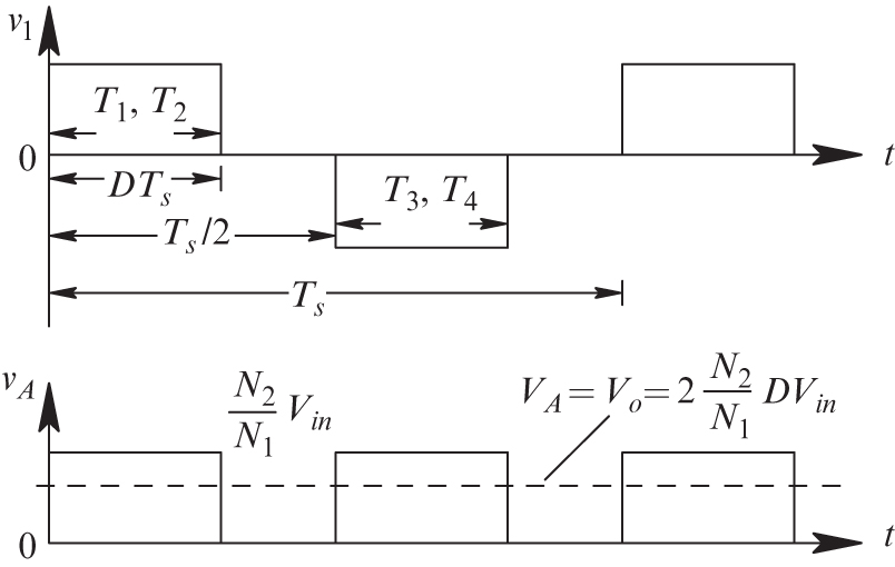
FIGURE 8.29 Full-bridge converter waveforms.
Interval ![]() with all transistors off. When all the transistors are turned off, there is no current in the primary winding, and the output inductor current divides equally (assuming an ideal transformer) between the two output diodes, as shown in the sub-circuit of Figure 8.28b. This ensures that the total ampere-turns acting on the transformer core equal zero because of
with all transistors off. When all the transistors are turned off, there is no current in the primary winding, and the output inductor current divides equally (assuming an ideal transformer) between the two output diodes, as shown in the sub-circuit of Figure 8.28b. This ensures that the total ampere-turns acting on the transformer core equal zero because of ![]() coming out of the dotted terminal and
coming out of the dotted terminal and ![]() going into the dotted terminal. Applying Kirchhoff’s voltage law in the loop consisting of the two secondaries in Figure 8.27b shows that
going into the dotted terminal. Applying Kirchhoff’s voltage law in the loop consisting of the two secondaries in Figure 8.27b shows that ![]() . Since
. Since ![]() , the two voltages must be individually zero, and hence also the primary voltage
, the two voltages must be individually zero, and hence also the primary voltage ![]() :
:
During this interval, ![]() as plotted in Figure 8.29.
as plotted in Figure 8.29.
The above discussion completes the discussion of one-half switching cycle. The other half-cycle with ![]() on applies a negative voltage (
on applies a negative voltage (![]() ) across the primary winding for an interval
) across the primary winding for an interval ![]() and results in
and results in ![]() conducting and
conducting and ![]() reverse biased. During this interval,
reverse biased. During this interval, ![]() as before when the positive voltage was applied to the primary winding. The waveforms during this half-cycle are as plotted in Figure 8.29.
as before when the positive voltage was applied to the primary winding. The waveforms during this half-cycle are as plotted in Figure 8.29.
From Figure 8.29, recognizing that ![]() in the DC steady state,
in the DC steady state,
Example 8.9
In a full-bridge converter shown in Figure 8.25, ![]() ,
, ![]() , and
, and ![]() . This converter is operating in CCM with a switching frequency
. This converter is operating in CCM with a switching frequency ![]() and supplying an output load
and supplying an output load ![]() . The filter inductor has an inductance of
. The filter inductor has an inductance of ![]() . Assuming this converter to be lossless, calculate the waveforms associated with it.
. Assuming this converter to be lossless, calculate the waveforms associated with it.
Solution From Equation (8.19), the duty ratio ![]() , where
, where ![]() . The average currents are
. The average currents are ![]() and
and ![]() . The voltage waveforms are shown in Figure 8.14. The peak-peak ripple in the filter inductor current
. The voltage waveforms are shown in Figure 8.14. The peak-peak ripple in the filter inductor current ![]() can be calculated from the voltage waveforms in Figure 8.30,
can be calculated from the voltage waveforms in Figure 8.30,

FIGURE 8.30 Waveforms of the full-bridge converter of Example 8.3.
Therefore, the ![]() waveform is as shown in Figure 8.30, with a minimum of IL, min = Iout
waveform is as shown in Figure 8.30, with a minimum of IL, min = Iout ![]() and a maximum of
and a maximum of ![]() .
.
Taking the transformer turns ratio into account, the primary current ![]() and the input current
and the input current ![]() ramp from
ramp from ![]() to
to ![]() , and are zero when all the transistors are off.
, and are zero when all the transistors are off.
8.6.2 Simulation and Hardware Prototyping
The simulation of a PWM full-bridge converter is demonstrated by means of an example:
Example 8.10
In the full-bridge converter shown in Figure 8.25, ![]() ,
, ![]() ,
, ![]() , and
, and ![]() . It is operating in DC steady state under the following conditions:
. It is operating in DC steady state under the following conditions: ![]() ,
, ![]() , and
, and ![]() . The primary side has a magnetizing inductance of
. The primary side has a magnetizing inductance of ![]() and a leakage inductance of
and a leakage inductance of ![]() . For the switch and the diode, use the parameters given in the Appendix of Chapter 2. Simulate this converter using LTspice.
. For the switch and the diode, use the parameters given in the Appendix of Chapter 2. Simulate this converter using LTspice.
Solution⋓The simulation file used in this example is available on the accompanying website. The LTspice model is shown in Figure 8.31, and the steady-state waveforms from the simulation of this model are shown in Figure 8.32.

FIGURE 8.31 LTspice model.

FIGURE 8.32 LTspice simulation results.
The Workbench model for implementing the above example in hardware using the Sciamble lab kit is shown in Figure 8.33
FIGURE 8.33 Workbench model.
The steady-state waveforms from running the full-bridge converter using the Sciamble laboratory kit are shown in Figure 8.34. The step-by-step procedure for re-creating the above hardware implementation is presented in [5].

FIGURE 8.34 Workbench hardware results: (1) Input current, (2) T1, T4 switchnode voltage, (3) Secondary-side inductor current, (4) T2, T3 switch-node voltage, and (M) Transformer primary-side voltage.
8.7 HALF-BRIDGE AND PUSH-PULL CONVERTERS
Variations of full-bridge converters are shown in Figure 8.35. The half-bridge converter in Figure 8.35a consists of only two transistors but requires two split capacitors to form a DC input midpoint. It is sometimes used at slightly lower power levels compared to the full-bridge converter.

FIGURE 8.35 Half-bridge and push-pull converters.
The push-pull converter in Figure 8.35b has the advantage of having both transistors’ gates referenced to the low side of the input voltage. The penalty is in the transformer, where during the power transfer interval, only one-half of the primary winding and one-half of the secondary winding are utilized.
8.8 PRACTICAL CONSIDERATIONS
To provide electrical isolation between the input and the output, the feedback control loop should also have electrical isolation. There are several ways of providing this isolation, as discussed in Reference [6].
REFERENCES
- 1. “Flyback Converter Lab Manual.” https://sciamble.com/resources/pe-drives-lab/basic-pe/flyback-converter.
- 2. “Flyback Converter Snubber Design,” Ray Ridley. http://www.ridleyengineering.com/images/phocadownload/12_%20flyback_snubber_design.pdf.
- 3. “Flyback Converter Snubber Design Lab Manual.” https://sciamble.com/resources/pe-drives-lab/basic-pe/flyback-snubber-converter.
- 4. “Forward Converter Lab Manual.” https://sciamble.com/resources/pe-drives-lab/basic-pe/forward-converter.
- 5. “Full-Bridge Converter Lab Manual.” https://sciamble.com/resources/pe-drives-lab/basic-pe/full-bridge-converter.
- 6. N. Mohan, T.M. Undeland, and W.P. Robbins, Power Electronics: Converters, Applications and Design, 3rd Edition (New York: John Wiley & Sons, 2003).
PROBLEMS
Flyback Converters
In Problems 8.1 through 8.4, in a flyback converter, ![]() ,
, ![]() turns, and
turns, and ![]() turns. The self-inductance of winding 1 is
turns. The self-inductance of winding 1 is ![]() , and
, and ![]() . The output voltage is regulated at
. The output voltage is regulated at ![]() .
.
- 8.1 Calculate and draw the waveforms shown in Figure 8.3 along with the ripple current in the output capacitor if the load is 30 W.
- 8.2 For the same duty ratio as in Problem 8.1, calculate the critical power, which makes this converter operate at the border of incomplete and complete demagnetization modes.
- 8.3 Draw the waveforms, similar to those in Problem 8.1, in Problem 8.2.
- 8.4 Consider that a flyback converter is operating in the complete demagnetizing mode. Under this mode of operation, derive the voltage transfer ratio
 in terms of the transformer magnetizing inductance
  seen from the input-side winding, switching frequency
  , the duty ratio
  , and the load resistance
  .
.
Forward Converter
In Problems 8.5 through 8.7, in a forward converter, ![]() ,
, ![]() turns,
turns, ![]() turns, and
turns, and ![]() turns. The self-inductance of winding 1 is
turns. The self-inductance of winding 1 is ![]() , and the switching frequency
, and the switching frequency ![]() . The output voltage is regulated such that
. The output voltage is regulated such that ![]() . The output filter inductance is
. The output filter inductance is ![]() , and the output load is 30 W.
, and the output load is 30 W.
- 8.5 Calculate and draw the waveforms for
 ,
,  ,
,  , and
, and  in Figure 8.16b, where
  is the current drawn from the input, and
  is the current through the diode
  .
. - 8.6 If the maximum duty ratio needs to be increased to
 , calculate
  .
. - 8.7 Why is diode
 necessary in Figure 8.16b?
 - 8.8 Consider that a forward converter is operating in the discontinuous-conduction mode. Under this mode of operation, derive the voltage transfer ratio
 in terms of the circuit parameters.
Two-Switch Forward Converter
In Problems 8.9 and 8.10, in a two-switch forward converter, ![]() ,
, ![]() , and the switching frequency
, and the switching frequency ![]() . The output voltage is regulated such that
. The output voltage is regulated such that ![]() . The self-inductance of winding 1 is
. The self-inductance of winding 1 is ![]() , and the output filter inductance is
, and the output filter inductance is ![]() .
.
- 8.9 Calculate and draw waveforms if the output load is 200 W.
- 8.10 Why is the duty ratio in this converter limited to 0.5?
Full-Bridge Converter
- 8.11 In a full-bridge converter, shown in Figure 8.25,
 ,
,  , and
, and  . The output voltage is regulated by PWM such that
  . The output power
  , and the peak-peak ripple in the output inductor current is 10% of its average value at full load. Calculate the value of the filter inductor
  . Calculate and plot all the waveforms associated with this converter. Assume the transformer ideal and the flux waveform to be symmetric with the same positive and negative peak amplitudes.
Half-Bridge Converter
- 8.12 A regulated DC power supply similar to Problem 8.11 is implemented using a half-bridge topology, shown in Figure 8.35a, where
 . Calculate all the waveforms associated with this converter.
Comparison of MOSFETs in Full-Bridge and Half-Bridge Converters
- 8.13 Compare the voltage and current ratings of MOSFETs in full-bridge and half-bridge converters of Problems 8.11 and 8.12 respectively.
Push-Pull Converter
- 8.14 A regulated DC power supply similar to Problem 8.11 is implemented using a push-pull topology shown in Figure 8.35b, where
 . Calculate all the waveforms associated with this converter.
Simulation Problems
- 8.15 Simulate a flyback converter with the following parameters and operating conditions:
 ,
,  ,
,  ,
,  , the output capacitance
  and the switching frequency
  .
.  .
.- Obtain the waveforms for
 ,
,  and
and  . What is the relationship between
  and
and  at the time of transition from the switch to diode, and vice versa?
 - What is the value of
 in this converter?
 - For
 , obtain the waveforms for
  ,
,  and
and  .
.
- Obtain the waveforms for
- 8.16 Simulate a forward converter with the following parameters and operating conditions:
 ,
,  ,
,  ,
,  , the filter inductor
  and the output capacitance
  , and the switching frequency
  .
.  .
.- Obtain the waveforms for
 ,
,  ,
,  ,
,  , and
, and  . What is the relationship between
  ,
,  , and
, and  at the time of transitions when the switch turns on, turns off, and the core gets demagnetized?
 - What is the voltage across the switch?
- What is the value of
 in this converter?
 - For
 , obtain the waveforms for
  ,
,  ,
,  ,
,  , and
, and  .
.
- Obtain the waveforms for
- 8.17 Simulate a full-bridge converter, with a midpoint rectifier, shown in Figure 8.25, with the following parameters and operating conditions:
 ,
,  ,
,  ,
,  , the filter inductor
  and the output capacitance
  , and the switching frequency
  .
.  .
.- Obtain the waveforms for
 ,
,  ,
,  ,
,  , and
, and  . What are their values when all switches are off?
 - Plot the waveforms of
 ,
,  ,
,  , and
, and  defined in Figure 8.28. What are their values when all switches are off?
 - Based on the converter parameters and the operating conditions, calculate the peak-peak ripple current in
 and verify your answer with the simulation results.
- Obtain the waveforms for