
2
DESIGN OF SWITCHING POWER-POLES
In the previous chapter, we discussed the role of power electronics in energy sustainability. Power electronics is an applied field of study where theory must be translated into practice to realize the immediate challenges that we face. We also discussed a switching power-pole as the building block of power electronic converters, consisting of an ideal bi-positional switch with an ideal transistor and an ideal diode and pulse-width modulation (PWM) to control the output. In this chapter, we will discuss the availability of various power semiconductor devices that are essential in power electronic systems, their switching characteristics, and various trade-offs in designing a switching power-pole, which can be used in various applications discussed in Chapter 1. We will also briefly discuss a PWM-IC, which is used in regulating and controlling the average output of such switching power-poles.
2.1 POWER TRANSISTORS AND POWER DIODES [1]
The power-level diodes and transistors have evolved over decades from their signal-level counterparts to the extent that they can handle voltages and currents in kilovolts and kiloamperes, respectively, with fast switching times of the order of a few tens of ![]() to a few
to a few ![]() . Moreover, these devices can be connected in series and parallel to satisfy any voltage and current requirements.
. Moreover, these devices can be connected in series and parallel to satisfy any voltage and current requirements.
The selection of power diodes and power transistors in a given application is based on the following characteristics:
- Voltage rating: The maximum instantaneous voltage that the device is required to block in its off state, beyond which it breaks down, that is, irreversible damage occurs.
- Current rating: The maximum current, expressed as instantaneous, average, and/or RMS, that a device can carry in its on state, beyond which excessive heating within the device destroys it.
- Switching speeds: The speeds with which a device can make a transition from its on state to off state, or vice versa. Small switching times associated with fast-switching devices result in low switching losses, or considering it differently, fast-switching devices can be operated at high switching frequencies with acceptable switching power losses.
- On-state voltage: The voltage drop across a device during its on state while conducting a current. The smaller this voltage, the smaller will be the on-state power loss.
2.2 SELECTION OF POWER TRANSISTORS [2–5]
Transistors are controllable switches, which are available in several forms for switch-mode power electronics applications:
- MOSFETs (metal-oxide-semiconductor field-effect transistors)
- IGBTs (insulated-gate bipolar transistors)
- IGCTs (integrated gate-commutated thyristors)
- GTOs (gate turn-off thyristors)
- Niche devices for power electronics applications, such as BJTs (bipolar junction transistors), SITs (static induction transistors), MCTs (MOS-controlled thyristors), and so on.
In switch-mode converters, there are two types of transistors that are primarily used: MOSFETs are typically used below a few hundred volts at switching frequencies in excess of 100 kHz, whereas IGBTs dominate very large voltage, current, and power ranges extending to MW levels, provided the switching frequencies are below a few tens of kHz. IGCTs and GTOs are used in utility applications of power electronics at power levels beyond a few MWs. Figure 1.25 shows the capabilities and applications of SiC- and GaN-based devices.
The following subsections provide a brief overview of MOSFET and IGBT characteristics and capabilities.
2.2.1 MOSFETs
In applications at voltages below 200 ![]() and switching frequencies in excess of 100 kHz,MOSFETs are clearly the device of choice because of their low on-state losses in low voltage ratings, their fast switching speeds, and a high-impedance gate that requires a small voltage and charge to facilitate the on/off transition. The circuit symbol of an n-channel MOSFET is shown in Figure 2.1a. It consists of three terminals: drain (D), source (S), and gate (G). The forward current in a MOSFET flows from the drain to the source terminal. MOSFETs can block only the forward polarity voltage; that is, a positive
and switching frequencies in excess of 100 kHz,MOSFETs are clearly the device of choice because of their low on-state losses in low voltage ratings, their fast switching speeds, and a high-impedance gate that requires a small voltage and charge to facilitate the on/off transition. The circuit symbol of an n-channel MOSFET is shown in Figure 2.1a. It consists of three terminals: drain (D), source (S), and gate (G). The forward current in a MOSFET flows from the drain to the source terminal. MOSFETs can block only the forward polarity voltage; that is, a positive ![]() . They cannot block a negative polarity voltage due to an intrinsic antiparallel diode, which can be used effectively in most switch-mode converter designs. MOSFET I-V characteristics for various gate voltage values are shown in Figure 2.1b.
. They cannot block a negative polarity voltage due to an intrinsic antiparallel diode, which can be used effectively in most switch-mode converter designs. MOSFET I-V characteristics for various gate voltage values are shown in Figure 2.1b.

FIGURE 2.1 MOSFET: (a) symbol, (b) I-V characteristics, (c) transfer characteristic.
For gate voltages below a threshold value ![]() , typically in the range of 2 to 4 V, a MOSFET is completely off, as shown by the I-V characteristics in Figure 2.1b, and approximates an open switch. Beyond
, typically in the range of 2 to 4 V, a MOSFET is completely off, as shown by the I-V characteristics in Figure 2.1b, and approximates an open switch. Beyond ![]() , the drain current
, the drain current ![]() through the MOSFET depends on the applied gate voltage
through the MOSFET depends on the applied gate voltage ![]() , as shown by the transfer characteristic shown in Figure 2.1c, which is valid almost for any value of the voltage
, as shown by the transfer characteristic shown in Figure 2.1c, which is valid almost for any value of the voltage ![]() across the MOSFET (note the horizontal nature of I-V characteristics in Figure 2.1b). To carry
across the MOSFET (note the horizontal nature of I-V characteristics in Figure 2.1b). To carry ![]() would require a gate voltage of a value at least equal to
would require a gate voltage of a value at least equal to ![]() , as shown in Figure 2.1c. Typically, a higher gate voltage, approximately 10 V, is maintained in order to keep the MOSFET in its on state and carrying
, as shown in Figure 2.1c. Typically, a higher gate voltage, approximately 10 V, is maintained in order to keep the MOSFET in its on state and carrying ![]() .
.
In its on state, a MOSFET approximates a very small resistor ![]() , and the drain current that flows through it depends on the external circuit in which it is connected. The on-state resistance, the inverse of the slope of I-V characteristics as shown in Figure 2.1b, is a strong function of the blocking voltage rating
, and the drain current that flows through it depends on the external circuit in which it is connected. The on-state resistance, the inverse of the slope of I-V characteristics as shown in Figure 2.1b, is a strong function of the blocking voltage rating ![]() of the device:
of the device:
The relationship in Equation 2.1 explains why MOSFETs in low-voltage applications, at less than 200 V, are an excellent choice. The on-state resistance goes up with the junction temperature within the device, and proper heatsinking must be provided to keep the temperature below the design limit.
2.2.2 IGBTs
IGBTs combine ease of control, as in MOSFETs, with low on-state losses even at fairly high voltage ratings. Their switching speeds are sufficiently fast for switching frequencies up to 30 kHz. Therefore, they are used for converters in a vast voltage and power range—from a fractional kilowatt to several megawatts where switching frequencies required are below a few tens of kilohertz.
The circuit symbol for an IGBT is shown in Figure 2.2a, and the I-V characteristics are shown in Figure 2.2b. Similar to MOSFETs, IGBTs have a high impedance gate, which requires only a small amount of energy to switch the device. IGBTs have a small on-state voltage, even in devices with a large blocking-voltage rating, for example, ![]() is approximately 2 V in 1200-V devices.
is approximately 2 V in 1200-V devices.
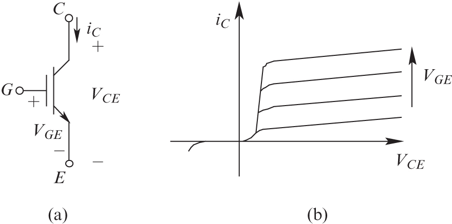
FIGURE 2.2 IGBT: (a) symbol, (b) I-V characteristics.
IGBTs can be designed to block negative voltages, but most commercially available devices, by design to improve other properties, cannot block any appreciable reverse polarity voltage. IGBTs have turn-on and turn-off times on the order of a microsecond and are available as modules in ratings as large as 3.3 kV and 1200 A. Voltage ratings of up to 5 kV are projected.
2.2.3 Power-Integrated Modules and Intelligent-Power Modules [2–4]
Power electronic converters, for example, for three-phase AC drives, require six power transistors. Power-integrated modules (PIMs) combine several transistors and diodes in a single package. Intelligent-power modules (IPMs) include power transistors with the gate-drive circuitry. The input to this gate-drive circuitry is a signal that comes from a microprocessor or an analog integrated circuit, and the output drives the MOSFET gate. IPMs also include fault protection and diagnostics, thereby immensely simplifying the power electronics converter design.
2.2.4 Costs of MOSFETs and IGBTs
As these devices evolve, their relative costs continue to decline. The costs of single devices are approximately 0.25 cents/A for 600-V devices and 0.50 cents/A for 1200-V devices. Power modules for the 3 kV class of devices cost approximately 1 cent/A.
2.3 SELECTION OF POWER DIODES
The circuit symbol of a diode is shown in Figure 2.3a, and its I-V characteristic in Figure 2.3b shows that a diode is an uncontrolled device that blocks reverse polarity voltage. Power diodes are available in large ranges of reverse voltage blocking and forward current carrying capabilities. Similar to transistors, power diodes are available in several forms as follows, and their selection must be based on their application:
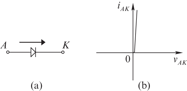
FIGURE 2.3 Diode: (a) symbol, (b) I-V characteristic.
- Line-frequency diodes
- Fast-recovery diodes
- Schottky diodes
- SiC-based Schottky diodes
Rectification of line-frequency AC to DC can be accomplished by slower switching p-n junction power (line-frequency) diodes, which have relatively a slightly lower on-state voltage drop and are available in voltage ratings of up to 9 kV and current ratings of up to 5 kA. The on-state voltage drop across these diodes is usually on the order of 1 to 3 V, depending on the voltage blocking capability.
Switch-mode converters operating at high switching frequencies, from several tens of kilohertz to several hundred kilohertz, require fast-switching diodes. In such applications, fast-recovery diodes, also formed by p-n junction as the line-frequency diodes, must be selected to minimize switching losses associated with the diodes.
In applications with very low output voltages, the forward voltage drop of approximately a volt across the conventional p-n junction diodes becomes unacceptably high. In such applications, another type of device called the Schottky diode is used with a voltage drop in the range of 0.3 to 0.5 V. Being majority-carrier devices, Schottky diodes switch extremely fast and keep switching losses to a minimum.
All devices, transistors, and diodes discussed above are silicon-based. Lately, silicon-carbide (SiC)–based Schottky diodes in voltage ratings of up to 1200 V have become available [6]. In spite of their large on-state voltage drop (1.7 V, for example), their capability to switch with a minimum of switching losses makes them attractive in converters with voltages in excess of a few hundred volts.
2.4 SWITCHING CHARACTERISTICS AND POWER LOSSES IN POWER POLES
In switch-mode converters, it is important to understand the switching characteristics of the switching power-pole. As discussed in the previous chapter, the power pole in a buck converter shown in Figure 2.4a is implemented using a transistor and a diode, where the current through the current port is assumed to be a constant DC, ![]() , for discussing switching characteristics. We will assume the transistor to be a MOSFET, although a similar discussion applies if an IGBT is selected.
, for discussing switching characteristics. We will assume the transistor to be a MOSFET, although a similar discussion applies if an IGBT is selected.

FIGURE 2.4 MOSFET in a switching power-pole.
For the n-channel MOSFET (p-channel MOSFETs have poor characteristics and are seldom used in power applications), the typical ![]() versus
versus ![]() characteristics are shown in Figure 2.4b for various gate voltages. The off-state and the on-state operating points are labeled on these characteristics.
characteristics are shown in Figure 2.4b for various gate voltages. The off-state and the on-state operating points are labeled on these characteristics.
Switching characteristics of MOSFETs, and hence of the switching power-pole in Figure 2.4a, are dictated by a combination of factors: the speed of charging and discharging of junction capacitances within the MOSFET, ![]() versus
versus ![]() characteristics, the circuit of Figure 2.4a in which the MOSFET is connected, and its gate-drive circuitry. We should note that the MOSFET junction capacitances are highly nonlinear functions of drain-source voltage and go up dramatically by several orders of magnitude at lower voltages. In Figure 2.4a, the gate-drive voltage for the MOSFET is represented as a voltage source, which changes from 0 to
characteristics, the circuit of Figure 2.4a in which the MOSFET is connected, and its gate-drive circuitry. We should note that the MOSFET junction capacitances are highly nonlinear functions of drain-source voltage and go up dramatically by several orders of magnitude at lower voltages. In Figure 2.4a, the gate-drive voltage for the MOSFET is represented as a voltage source, which changes from 0 to ![]() , approximately 10 V, and vice versa, and charges or discharges the gate through a resistance
, approximately 10 V, and vice versa, and charges or discharges the gate through a resistance ![]() that is the sum of external resistance
that is the sum of external resistance ![]() and the internal gate resistance.
and the internal gate resistance.
Only a simplified explanation of the turn-on and turn-off characteristics, assuming an ideal diode, is presented here. The switching details, including the diode reverse recovery, are discussed in the Appendix to this chapter.
2.4.1 Turn-On Characteristic
Prior to turn-on, Figure 2.5a shows the circuit in which the MOSFET is off and blocks the input DC voltage ![]() ;
; ![]() freewheels through the diode. By applying a positive voltage to the gate, the turn-on characteristic describes how the MOSFET goes from the off-point to the on-point in Figure 2.5b. To turn the MOSFET on, the gate-drive voltage goes up from 0 to
freewheels through the diode. By applying a positive voltage to the gate, the turn-on characteristic describes how the MOSFET goes from the off-point to the on-point in Figure 2.5b. To turn the MOSFET on, the gate-drive voltage goes up from 0 to ![]() , and it takes the gate drive a finite amount of time, called the turn-on delay time
, and it takes the gate drive a finite amount of time, called the turn-on delay time ![]() , to charge the gate-source capacitance through the gate-circuit resistance
, to charge the gate-source capacitance through the gate-circuit resistance ![]() to the threshold value of
to the threshold value of ![]() . During this turn-on delay time, the MOSFET remains off and
. During this turn-on delay time, the MOSFET remains off and ![]() continues to freewheel through the diode, as shown in Figure 2.5a.
continues to freewheel through the diode, as shown in Figure 2.5a.

FIGURE 2.5 MOSFET turn-on.
For the MOSFET to turn on, first, the current ![]() through it rises. As long as the diode is conducting a positive net current
through it rises. As long as the diode is conducting a positive net current ![]() , the voltage across it is zero, and the MOSFET must block the entire input voltage
, the voltage across it is zero, and the MOSFET must block the entire input voltage ![]() . Therefore, during the current rise time
. Therefore, during the current rise time ![]() , the MOSFET voltage and the current are along the trajectory A in the I-V characteristics of Figure 2.5b and are plotted in Figure 2.5c. Once the MOSFET current reaches
, the MOSFET voltage and the current are along the trajectory A in the I-V characteristics of Figure 2.5b and are plotted in Figure 2.5c. Once the MOSFET current reaches ![]() , the diode becomes reverse biased, and the MOSFET voltage falls. During the voltage fall time
, the diode becomes reverse biased, and the MOSFET voltage falls. During the voltage fall time ![]() , as depicted by the trajectory B in Figure 2.5b and the plots in Figure 2.5c, the gate-to-source voltage remains at
, as depicted by the trajectory B in Figure 2.5b and the plots in Figure 2.5c, the gate-to-source voltage remains at ![]() . Once the turn-on transition is complete, the gate charges to the gate-drive voltage
. Once the turn-on transition is complete, the gate charges to the gate-drive voltage ![]() , as shown in Figure 2.5c.
, as shown in Figure 2.5c.
Example 2.1
In the converter of Figure 2.4a, the transistor is a MOSFET that carries a current of 5 A when it is fully on. If the current through the transistor is to be limited to 40 A during a malfunction, in which case the entire input voltage of 50 V appears across the transistor, what should be the maximum on-state gate voltage that the gate-drive circuit should provide? Assume the junction temperature ![]() of the MOSFET to be 175 °C.
of the MOSFET to be 175 °C.
Solution The transfer characteristic of this MOSFET is shown in Figure 2.6. It shows that if ![]() is used, the current through the MOSFET will be limited to 40 A.
is used, the current through the MOSFET will be limited to 40 A.
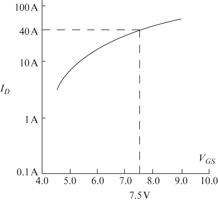
FIGURE 2.6 MOSFET transfer characteristic.
2.4.2 Turn-Off Characteristic
The turn-off sequence is the opposite of the turn-on process. Prior to turn-off, the MOSFET is conducting ![]() , and the diode is reverse biased, as shown in Figure 2.7a. The MOSFET I-V characteristics are replotted in Figure 2.7b. The turn-off characteristic describes how the MOSFET goes from the on-point to the off-point in Figure 2.7b. To turn the MOSFET off, the gate-drive voltage goes down from
, and the diode is reverse biased, as shown in Figure 2.7a. The MOSFET I-V characteristics are replotted in Figure 2.7b. The turn-off characteristic describes how the MOSFET goes from the on-point to the off-point in Figure 2.7b. To turn the MOSFET off, the gate-drive voltage goes down from ![]() to
to ![]() . It takes the gate drive a finite amount of time, called the turn-off delay time
. It takes the gate drive a finite amount of time, called the turn-off delay time ![]() , to discharge the gate-source capacitance through the gate-circuit resistance
, to discharge the gate-source capacitance through the gate-circuit resistance ![]() , from a voltage of
, from a voltage of ![]() to
to ![]() . During this turn-off delay time, the MOSFET remains on.
. During this turn-off delay time, the MOSFET remains on.

FIGURE 2.7 MOSFET turn-off.
For the MOSFET to turn off, the output current must be able to freewheel through the diode. This requires the diode to become forward biased, and thus the voltage across the MOSFET must rise, as shown by the trajectory C in Figure 2.7b, while the current through it remains ![]() . During this voltage rise time
. During this voltage rise time ![]() , the voltage and current are plotted in Figure 2.7c, while the gate-to-source voltage remains at
, the voltage and current are plotted in Figure 2.7c, while the gate-to-source voltage remains at ![]() . Once the voltage across the MOSFET reaches
. Once the voltage across the MOSFET reaches ![]() , the diode becomes forward biased, and the MOSFET current falls. During the current fall time
, the diode becomes forward biased, and the MOSFET current falls. During the current fall time ![]() , depicted by the trajectory D in Figure 2.7b and the plots in Figure 2.7c, the gate-to-source voltage declines to
, depicted by the trajectory D in Figure 2.7b and the plots in Figure 2.7c, the gate-to-source voltage declines to ![]() . Once the turn-off transition is complete, the gate discharges to
. Once the turn-off transition is complete, the gate discharges to ![]() .
.
2.4.3 Calculating Power Losses within the MOSFET (Assuming an Ideal Diode)
Power losses in the gate-drive circuitry are negligibly small except at very high switching frequencies. The primary source of power losses is across the drain and the source, which can be divided into two categories: the conduction loss and the switching losses. Both of these are discussed in the following sections.
2.4.3.1 Conduction Loss
In the on-state, the MOSFET conducts a drain current for an interval ![]() during every switching time period
during every switching time period ![]() , with the switch duty ratio
, with the switch duty ratio ![]() . Assuming this current to be at a constant
. Assuming this current to be at a constant ![]() during
during ![]() , since it is zero during the rest of the switching time period, the RMS value of the MOSFET current is
, since it is zero during the rest of the switching time period, the RMS value of the MOSFET current is
Hence, the average power loss in the on-state resistance ![]() of the MOSFET is
of the MOSFET is
As pointed out earlier, ![]() varies significantly with the junction temperature, and data sheets often provide its value at the junction temperature equal to 25 °C. However, it will be more realistic to use twice this resistance value, which corresponds to the junction temperature equal to 120 °C, for example. Equation 2.3 can be refined to account for the effect of a ripple in the drain current on the conduction loss. The conduction loss is highest at the maximum load on the converter when the drain current would also be at its maximum.
varies significantly with the junction temperature, and data sheets often provide its value at the junction temperature equal to 25 °C. However, it will be more realistic to use twice this resistance value, which corresponds to the junction temperature equal to 120 °C, for example. Equation 2.3 can be refined to account for the effect of a ripple in the drain current on the conduction loss. The conduction loss is highest at the maximum load on the converter when the drain current would also be at its maximum.
2.4.3.2 Switching Losses
At high switching frequencies, switching power losses can be even higher than the conduction loss. The switching waveforms for the MOSFET voltage ![]() and the current
and the current ![]() , corresponding to the turn-on and the turn-off trajectories in Figures 2.5 and 2.7, assuming they are linear with time, are replotted in Figure 2.8.
, corresponding to the turn-on and the turn-off trajectories in Figures 2.5 and 2.7, assuming they are linear with time, are replotted in Figure 2.8.
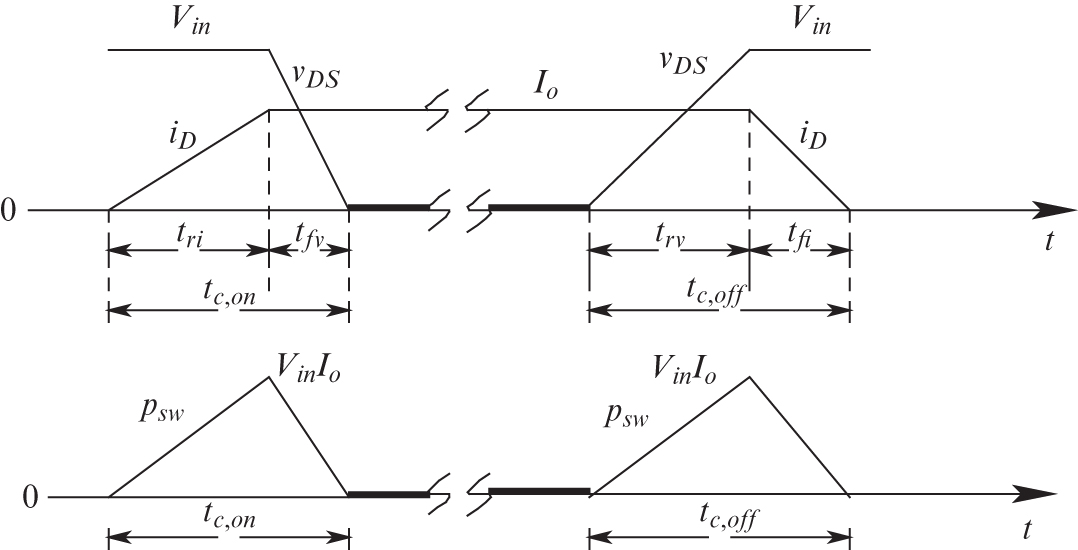
FIGURE 2.8 MOSFET switching losses.
During each transition from on to off, and vice versa, the transistor has simultaneously high voltage and current, as seen from the switching waveforms in Figure 2.8. The instantaneous power loss ![]() in the transistor is the product of
in the transistor is the product of ![]() and
and ![]() , as plotted. The average value of the switching losses from the plots in Figure 2.8 is
, as plotted. The average value of the switching losses from the plots in Figure 2.8 is
where ![]() and
and ![]() are defined in Figure 2.8 as the sum of the rise and the fall times associated with the MOSFET voltage and current:
are defined in Figure 2.8 as the sum of the rise and the fall times associated with the MOSFET voltage and current:
2.4.4 Gate Driver Integrated Circuits (ICs) with Built-in Fault Protection [2]
Application-specific ICs (ASICs) for controlling the gate voltages of MOSFETs and IGBTs greatly simplify converter design by including various protection features, for example, the over-current protection that turns off the transistor under fault conditions. This functionality, as discussed earlier, is integrated into intelligent-power modules along with the power semiconductor devices.
The IC to drive the MOSFET gate is shown in Figure 2.9 in a block diagram form. To drive the high-side MOSFET in the power pole, the input signal ![]() from the controller is referenced to the logic level ground,
from the controller is referenced to the logic level ground, ![]() is the logic supply voltage, and
is the logic supply voltage, and ![]() to drive the gate is supplied by an isolated power supply referenced to the MOSFET source S.
to drive the gate is supplied by an isolated power supply referenced to the MOSFET source S.

FIGURE 2.9 Gate-driver IC functional diagram
One of the ICs for this purpose is UCC21710, which can source up to 10 A for gate charging and sink up to 10 A for gate discharging. It has built-in overcurrent fault protection capability, in which the transistor current, measured via the voltage drop across a small resistance in series with the transistor, disables the gate-drive voltage under over-current conditions.
For extremely low-cost designs, the bootstrap driver shown in Figure 2.10a is a suitable alternative to the more expensive optically or galvanically isolated gate driver. These are suitable for converters with a pair of series-connected devices that are driven in a complementary manner.

FIGURE 2.10 Bootstrap gate-driver circuit and operation
Unlike an isolated gate driver, which requires an isolated power supply to source the buffer that drives the high-side switch ![]() in Figure 2.10a, the bootstrap driver uses the energy stored in the capacitor
in Figure 2.10a, the bootstrap driver uses the energy stored in the capacitor ![]() to source the buffer. This capacitor is charged up during the normal operation of the converter. When
to source the buffer. This capacitor is charged up during the normal operation of the converter. When ![]() is off and
is off and ![]() is on, the capacitor is charged from the input DC power supply, as shown in Figure 2.10b. The resistor
is on, the capacitor is charged from the input DC power supply, as shown in Figure 2.10b. The resistor ![]() limits the current flowing into the capacitor, and the voltage across the capacitor is clamped using an active circuit typically present within the driver or using an external Zener diode. When
limits the current flowing into the capacitor, and the voltage across the capacitor is clamped using an active circuit typically present within the driver or using an external Zener diode. When ![]() turns off, the diode
turns off, the diode ![]() gets reverse biased. Thus, the voltage across
gets reverse biased. Thus, the voltage across ![]() is available for the buffer of
is available for the buffer of ![]() to source the gate turn on. During this interval, the capacitor gets discharged, as shown in Figure 2.10c.
to source the gate turn on. During this interval, the capacitor gets discharged, as shown in Figure 2.10c.
There are a few shortcomings associated with bootstrap drives. The maximum on-time of the high-side device is limited so as to provide enough time for the bootstrap capacitor to charge. It lowers the overall efficiency due to the power loss associated with ![]() during every charging cycle, which is more pronounced at high voltages, and limits its use to mostly converters operating within 100 V.
during every charging cycle, which is more pronounced at high voltages, and limits its use to mostly converters operating within 100 V.
2.5 JUSTIFYING SWITCHES AND DIODES AS IDEAL
Product reliability and high energy efficiency are two very important criteria. In designing converters, it is essential that in the selection of semiconductor devices, we consider their voltage and current ratings with proper safety margins for reliability purposes. Achieving high energy efficiency from converters requires that in selecting power devices, we consider their on-state voltage drops and their switching characteristics. We also need to calculate the heat that needs to be removed for proper thermal design.
Typically, the converter energy efficiency of approximately 90% or higher is realized. This implies that semiconductor devices have a very small loss associated with them. Therefore, in analyzing various converter topologies and comparing them against each other, we can assume transistors and diodes are ideal. Their non-idealities, although essential to consider in the actual selection and the subsequent design process, represent second-order phenomena that will be ignored in analyzing various converter topologies. We will use a generic symbol shown earlier for transistors, regardless of their type, and ignore the need for a specific gate-drive circuitry.
2.6 DESIGN CONSIDERATIONS
In designing any converter, the overall objectives are to optimize its cost, size, weight, energy efficiency, and reliability. With these goals in mind, we will briefly discuss some important considerations as the criteria for selecting the topology and the components in a given application.
2.6.1 Switching Frequency fs
As discussed in the buck converter example of the previous chapter, a switching power-pole results in a waveform pulsating at a high switching frequency at the current port. The high-frequency components in the pulsating waveform need to be filtered. It is intuitively obvious that the benefits of increasing the switching frequencies lie in reducing the filter component values, ![]() and
and ![]() , and hence their physical sizes in a converter. (This is true up to a certain value, up to a few hundred kHz, beyond which, for example, magnetic losses in inductors and the internal inductance within capacitors reverse the trend.) Hence, higher switching frequencies allow a higher control bandwidth, as we will see in Chapter 4.
, and hence their physical sizes in a converter. (This is true up to a certain value, up to a few hundred kHz, beyond which, for example, magnetic losses in inductors and the internal inductance within capacitors reverse the trend.) Hence, higher switching frequencies allow a higher control bandwidth, as we will see in Chapter 4.
The negative consequences of increasing the switching frequency are in increasing the switching losses in the transistor and the diode, as discussed earlier. Higher switching frequencies also dictate a faster switching of the transistor by appropriately designed gate-drive circuitry, generating greater problems of electromagnetic interference due to higher di/dt and dv/dt that introduce switching noise in the control loop and the rest of the system. We can minimize these problems, at least in DC-DC converters, by adopting a soft-switching topology, discussed in Chapter 10.
2.6.2 Selection of Transistors and Diodes
Earlier, we discussed the voltage and the switching frequency ranges for selecting between MOSFETs and IGBTs. Similarly, the diode types should be chosen appropriately. The voltage rating of these devices is based on the peak voltage ![]() in the circuit (including voltage spikes due to parasitic effects during switching). The current ratings should consider the peak current
in the circuit (including voltage spikes due to parasitic effects during switching). The current ratings should consider the peak current ![]() that the devices can handle, which dictates the switching power loss, the RMS current
that the devices can handle, which dictates the switching power loss, the RMS current ![]() for MOSFETs, which behave as a resistor with
for MOSFETs, which behave as a resistor with ![]() in their on-state, and the average current
in their on-state, and the average current ![]() for IGBTs and diodes, which can be approximated to have a constant on-state voltage drop. Safety margins, which depend on the application, dictate that the device ratings be greater than the worst-case stresses by a certain factor.
for IGBTs and diodes, which can be approximated to have a constant on-state voltage drop. Safety margins, which depend on the application, dictate that the device ratings be greater than the worst-case stresses by a certain factor.
2.6.3 Magnetic Components
As discussed earlier, the filter inductance value depends on the switching frequency. Inductor design, discussed later in Chapter 9, shows that the physical size of a filter inductor, to a first approximation, depends on a quantity called the area-product (![]() ) given by the equation below:
) given by the equation below:
Increasing ![]() in many topologies reduces the peak and the RMS values (also reducing the transistor and the diode current stresses) but has the negative consequence of increasing the overall inductor size and possibly reducing the control bandwidth.
in many topologies reduces the peak and the RMS values (also reducing the transistor and the diode current stresses) but has the negative consequence of increasing the overall inductor size and possibly reducing the control bandwidth.
2.6.4 Capacitor Selection [7]
Capacitors have switching losses designated by equivalent series resistance, ESR, as shown in Figure 2.11. They also have an internal inductance, represented as an equivalent series inductance, ESL. The resonance frequency, the frequency beyond which ESL begins to dominate C, depends on the capacitor type. Electrolytic capacitors offer high capacitance per unit volume but have low resonance frequency. On the other hand, capacitors such as ceramic and metal-polypropylene have relatively high resonance frequency. Therefore, in switch-mode DC power supplies, an electrolytic capacitor with high C may often be paralleled with a ceramic or metal-polyester capacitor to form the output filter capacitor.

FIGURE 2.11 Capacitor ESR and ESL.
2.6.5 Thermal Design [8, 9]
The power dissipated in the semiconductor and the magnetic devices must be removed to limit temperature rise within the device. The reliability of converters and their life expectancy depends on the operating temperatures, which should be well below their maximum allowed values. On the other hand, letting them operate at a high temperature decreases the cost and the size of the heat sinks required. There are several cooling techniques, but for general-purpose applications, converters are often designed for cooling by normal air convection without the use of forced air or liquid.
Semiconductor devices come in a variety of packages, which differ in cost, ruggedness, thermal conduction, and radiation hardness if the application demands it. Figure 2.12a shows a semiconductor device affixed to a heat sink through an isolation pad that is thermally conducting but provides electrical isolation between the device case and the heat sink.

FIGURE 2.12 Thermal design: (a) semiconductor on a heat sink, (b) electrical analog.
An analogy can be drawn with an electrical circuit, as shown in Figure 2.12b, where the power dissipation within the device is represented as a DC current source, thermal resistances offered by various paths are represented as series resistances, and the temperatures at various points as voltages. The data sheets specify various thermal resistance values. The heat transfer mechanism is primarily conduction from the semiconductor device to its case and through the isolation pad. The resulting thermal resistances can be represented by![]() and
and ![]() , respectively. From the heat sink to the ambient, the heat transfer mechanisms are primarily convection and radiation, and the thermal resistance can be represented by
, respectively. From the heat sink to the ambient, the heat transfer mechanisms are primarily convection and radiation, and the thermal resistance can be represented by ![]() . Based on the electrical analogy, the junction temperature can be calculated as follows for the dissipated power
. Based on the electrical analogy, the junction temperature can be calculated as follows for the dissipated power ![]() :
:
2.6.6 Design Trade-Offs
As a function of switching frequency, Figure 2.13 qualitatively shows the plot of physical sizes for the magnetic components and the capacitors and the heat sink. Based on the present state of the art, optimum values of switching frequencies to minimize the overall size in DC-DC converters using MOSFETs range from 200 kHz to 300 kHz with a slight upward trend.

FIGURE 2.13 Size of magnetic components and heat sink as a function of frequency.
2.7 THE PWM IC
In the pulse-width modulation of the power pole in a DC-DC converter, a high-speed PWM IC such as the UC3824 from Unitrode/Texas Instruments may be used. Functionally within this PWM IC, the control voltage ![]() generated by the controller is compared with a ramp signal
generated by the controller is compared with a ramp signal ![]() of amplitude
of amplitude ![]() , at a constant switching frequency
, at a constant switching frequency ![]() , as shown in Figure 2.14. The output switching signal represents the transistor switching function
, as shown in Figure 2.14. The output switching signal represents the transistor switching function ![]() , which equals 1 if
, which equals 1 if ![]() and 0 otherwise. The transistor duty ratio based on Figure 2.14 is given as
and 0 otherwise. The transistor duty ratio based on Figure 2.14 is given as

FIGURE 2.14 PWM IC waveforms.
Thus, the control voltage ![]() can provide regulation of the average output voltage of the switching power-pole, as discussed further in Chapters 3 and 4.
can provide regulation of the average output voltage of the switching power-pole, as discussed further in Chapters 3 and 4.
Many application-specific ICs can be found in [10]. One such IC is UCC28704, which is used to control the transistor in a flyback converter. The IC does not require an optocoupler feedback circuit, instead relying on auxiliary winding to accurately sense the output voltage at the end of demagnetization. The IC also offers quasi-resonant switching where the transistor is turned on at the valley of ringing transistor voltage during discontinuous conduction mode, as explained in Chapter 8. UCC2897A is a controller IC to control a forward converter, also described in Chapter 8. This controller works with an active-clamp forward converter, which eliminates the need for a demagnetization winding to reset the transformer core, making it more compact and efficient.
With the cost of programmable digital controllers rapidly declining, especially ones that support floating-point operation, it is becoming more common to use a programmable digital controller for controlling power electronic converters instead of relying on specific ICs mentioned earlier. One such controller is the Texas Instruments TMS320F280049 DSP. It comes with built-in peripherals such as 14 ADCs, 2 DACs, and 16 PWMs. It has slope generation for internal comparators’ DAC for easy implementation of peak current control, as described in Chapter 4. Most PWM peripherals support simple dead-time commutation needed for converters such as the synchronous-rectified buck converter, described in Chapter 3. More complex commutation logic usually requires either external logic ICs or FPGA for programmable logic. The TMS320F280049 DSP has an internal configurable logic block that allows for modifying the PWM signals or input capture signal for converters that require specialized commutation, such as matrix converters.
2.8 HARDWARE PROTOTYPING
All the components mentioned in this chapter are used in the associated Sciamble Power Electronics lab kit, shown in Figure 2.15. The kit consists of three switching power-poles. Two of the switching power-poles are each made up of onsemi’s FDMS8090. Each FDMS8090 consists of two 100 V, 10 A Si-MOSFETs. The third switching power-pole is made up of Texas Instruments’ LMG5200. LMG5200 is a GaN half-bridge IC, rated for 80 V, 10 A. Both the GaN and the Si switches are driven through a bootstrap driver, discussed in section 2.4.4.

FIGURE 2.15 Sciamble power electronic lab kit.
The switches are controlled using TMS320F280049 DSP, mentioned in section 2.7. The DSP is directly programmed using the Sciamble Workbench platform, which allows for developing real-time control using pre-built drag-and-drop toolboxes without any need for C programming or DSP-specific knowledge.
As mentioned in section 2.6.4, the input and output power stages of the lab kit are each decoupled using a single 470 µF capacitor and paralleled with two low ESR 10 µF ceramic capacitors.
Depending on the converter under consideration, the different magnetics sub-circuits, shown in Figure 2.15, are used either with the Si or the GaN power pole, as demonstrated in the following chapters.
The datasheet of all the components used in the Sciamble lab kit, as well as in all the LTspice models in the following chapters, is provided in the Appendix on the accompanying website.
REFERENCES
- 1. N. Mohan, T.M. Undeland, and W.P. Robbins, Power Electronics: Converters, Applications and Design, 3rd Edition (New York: John Wiley & Sons, 2003).
- 2. International Rectifier. http://www.irf.com.
- 3. POWEREX Corporation.: http://www.pwrx.com.
- 4. Fuji Semiconductor. http://www.fujisemiconductor.com.
- 5. On Semiconductor. http://www.onsemiconductor.com.
- 6. Infineon Technologies. http://www.infineon.com.
- 7. Panasonic Capacitors. http://www.panasonic.com/industrial/electronic-components/capacitive-products.
- 8. Boyd (Formerly Aavid, Thermal Division of Boyd Corp), for heat sinks, http://boydcorp.com/aavid.html.
- 9. Bergquist Company for thermal pads.: http://www.bergquistcompany.com.
- 10. PWM Controller ICs.: https://www.ti.com/power-management/acdc-isolated-dcdc-switching-regulators/pwm-controllers/overview.html.
PROBLEMS
MOSFET in a Power Pole of Figure 2.4a (Problems 2.1 through 2.8)
- 2.1 A MOSFET is used in a switching power-pole shown in Figure 2.4a. Assume the diode ideal. The operating conditions are as follows:
 ,
,  , the switching frequency
  , and the duty ratio
  . Under the operating conditions, the MOSFET has the following switching times:
  ,
,  ,
,  ,
,  ,
,  ,
,  . The on-state resistance of the MOSFET is
  . Assume
  as a step voltage between 0 V and 12 V.
- Draw and label the turn-on and turn-off characteristics of the MOSFET and sketch the MOSFET gate-source voltage
 waveform.
 - Draw and label the diode voltage and current waveforms, assuming it to be ideal.
- Draw and label the turn-on and turn-off characteristics of the MOSFET and sketch the MOSFET gate-source voltage
- 2.2 Plot the turn-on and the turn-off switching power losses in the MOSFET. Calculate the average switching power loss in the MOSFET.
- 2.3 Calculate the average conduction loss in the MOSFET.
- 2.4 Instead of an ideal diode, consider a real diode with a forward voltage drop
 . Calculate the average forward power loss in the diode.
 - 2.5 In the diode reverse recovery characteristic shown in Figure 2A.1,
 ,
,  , and
, and  . Calculate the average switching power loss in the diode.

FIGURE 2A.1 Diode reverse-recovery characteristic.
- 2.6 In the gate-drive circuitry of the MOSFET, assume that the external power supply
 in Figure 2.9 has a voltage of 12 V. To turn the MOSFET on each time, under the conditions given, requires a charge
  from the 12 V supply. Calculate the average gate-drive power loss, assuming that at turn-off of the MOSFET, no energy is returned to the 12 V supply.
 - 2.7 In this problem, we will calculate new values of the turn-on and the turn-off delay times of the MOSFET, based on the gate driver IC IR2127, as described in Section 2.4.4. This IC is supplied with a voltage
 with respect to the MOSFET source. Assume this voltage to equal
  . Also assume the internal series resistance of the MOSFET gate to be zero.
- For the turn-on, assume that this driver IC is a voltage source of
 with an internal resistance of
  in series. Calculate the turn-on delay time
  , assuming that the MOSFET threshold voltage
  . Assume the MOSFET capacitance to be 1800
  for this calculation.
 - For turning-off of the MOSFET, assume that this driver IC shorts the MOSFET gate to its source through an internal resistance of
 . Calculate the turn-off delay time
  , assuming that the MOSFET voltage
  . Assume the MOSFET capacitance to be 1800
  for this calculation.
- For the turn-on, assume that this driver IC is a voltage source of
- 2.8 The MOSFET losses are the sum of those computed in Problems 2.2 and 2.3. The junction temperature must not exceed
 , and the ambient temperature is given as
  . From the MOSFET datasheet,
  . The thermal pad has
  . Calculate the maximum value of
  that the heat sink can have.
Simulation Problem
- 2.9 To achieve the output capacitor in a buck converter, an electrolytic capacitor
 is connected in parallel with a polypropylene capacitor
  . Each of these capacitors has the following ESR and ESL as shown in Figure 2.10:
  ,
,  ,
,  and
and  .
.- Obtain the frequency response of the admittances associated with
 and
and  , and their parallel combination, in terms of their magnitude and the phase angles.
 - Obtain the resonance frequency for the two capacitors and their combination.
- Obtain the frequency response of the admittances associated with
Hint: Look at the phase plot.
APPENDIX 2A DIODE REVERSE RECOVERY AND POWER LOSSES
In this Appendix, the diode reverse-recovery characteristic is described and the associated power losses are calculated.
2A.1 Average Forward Loss in Diodes
The current flow through a diode results in a forward voltage drop ![]() across the diode. The average forward power loss
across the diode. The average forward power loss ![]() in the diode in the circuit of Figure 2.4a can be calculated as
in the diode in the circuit of Figure 2.4a can be calculated as
where ![]() is the MOSFET duty ratio in the power pole, and hence the diode conducts for (
is the MOSFET duty ratio in the power pole, and hence the diode conducts for (![]() ) portion of each switching time period.
) portion of each switching time period.
2A.2 Diode Reverse-Recovery Characteristic
Forward current in power diodes, unlike in majority-carrier Schottky diodes, is due to the flow of electrons as well as holes. This current results in an accumulation of electrons in the p-region and of holes in the n-region. The presence of these charges allows a flow of current in the negative direction that sweeps away these excess charges, and the negative current quickly comes to zero, as shown in the plot of Figure 2A.1.
The peak reverse recovery current ![]() and the reverse-recovery charge
and the reverse-recovery charge ![]() shown in Figure 2A.1 depend on the initial forward current
shown in Figure 2A.1 depend on the initial forward current ![]() and the rate
and the rate ![]() at which this current decreases.
at which this current decreases.
2A.3 Diode Switching Losses
The reverse recovery current results in switching losses within the diode when a negative current is flowing beyond the interval ![]() in Figure 2A.1, while the diode is blocking a negative voltage
in Figure 2A.1, while the diode is blocking a negative voltage ![]() . This switching power loss in the diode can be estimated from the plots of Figure 2A.1 as
. This switching power loss in the diode can be estimated from the plots of Figure 2A.1 as
where ![]() is the switching frequency. In switch-mode power electronics, increase in switching losses due to the diode reverse recovery can be significant, and diodes with ultra-fast reverse recovery characteristics are needed to avoid these from becoming excessive.
is the switching frequency. In switch-mode power electronics, increase in switching losses due to the diode reverse recovery can be significant, and diodes with ultra-fast reverse recovery characteristics are needed to avoid these from becoming excessive.
2A.4 Diode Switching Losses
The reverse recovery current of the diode also increases the turn-on losses in the associated MOSFET of the power-pole. This is illustrated by an example below.
Example 2.2
In the switching power-pole of Figure 2.4a, ![]() and the output current is
and the output current is ![]() . The switching frequency
. The switching frequency ![]() . The MOSFET switching times are
. The MOSFET switching times are ![]() . The diode snaps off at reverse recovery such that
. The diode snaps off at reverse recovery such that ![]() (such that
(such that ![]() ) and the peak reverse-recovery current
) and the peak reverse-recovery current ![]() . Calculate the additional power loss in the MOSFET due to the diode reverse recovery.
. Calculate the additional power loss in the MOSFET due to the diode reverse recovery.
Solution The waveforms are as shown in Figure 2A.2, where the drain current keeps rising for an additional value of ![]() , beyond
, beyond ![]() , during
, during ![]() . Beyond this interval, the drain-source voltage falls during the interval
. Beyond this interval, the drain-source voltage falls during the interval ![]() .
.

FIGURE 2A.2 Waveforms with diode reverse-recovery current.
With a near-ideal diode, as soon as the drain current reaches ![]() , the MOSFET voltage
, the MOSFET voltage ![]() begins to drop linearly in an interval
begins to drop linearly in an interval ![]() , and the corresponding switching loss in the MOSFET is shown cross-hatched:
, and the corresponding switching loss in the MOSFET is shown cross-hatched:
With the diode with a reverse-recovery current, the switching loss in the MOSFET is
Therefore, the additional power loss in the MOSFET is 0.68 W, which more than doubles the power loss in it.