
Chapter 2
Stereoscopic Displays
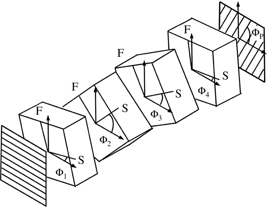
The viewer of stereoscopic displays has to use eye glasses. The two views required for 3D vision are obtained either by placing both views into the area of the screen, a method called area division multiplex, or by presenting the views as a time sequential display, also called time division multiplex. In the first approach each view can only exhibit half the resolution of a 2D display. Contrary to that, in the second approach the full resolution of a one-view display is maintained, but the addressing of the time sequential display must work at twice the speed of a regular 2D display.
For area division the light of the two views is polarized differently in order to distinguish the views. In case of a linear polarization, two perpendicular polarizations, crossed polarizations, are used, while circular polarization works with the right-handed and left-handed versions. The eye glasses have lenses, each of which allows only one of the polarizations to pass. So the right eye perceives only the image with one type of polarization and the left eye only the image with the other type of polarization. The solutions with area division differ in the way they create the second polarization from a given first one.
The eye glasses for the time division approach can also operate without polarization as shutter glasses in an on–off mode. While the image for the right eye is displayed, the right eye lens is transparent and the left eye lens opaque, and vice versa for the left eye. The next section is devoted to area division, followed by a section on time division.
2.1 Stereoscopic Displays with Area Multiplexing
The generation of the second polarization from a given polarization is achieved either by using a retarder or a wire grid polarizer (WGP), where the latter is often also complemented by an additional retarder. The two approaches are treated below in separate sections.
2.1.1 Retarders for the Generation of Polarizations
The two views are realized in Figure 2.1 by an LCD with a patterned structure of row-wise different images for the right eye indicated by R and interleaved by rows for the left eye indicated by L [1]. The rows exhibit the full resolution of a regular TV image, so high definition (HD) or full high definition (FHD) can be realized in the rows, while the columns have to present two views, each with half the resolution. The backlight is linearly polarized with an angle of 45°. A microretarder film rotates the polarization for the right eye by π/2, which corresponds to a retardation of λ/2, where λ is the wavelength. There is no rotation for the left eye images. The two images now have crossed polarization.
Figure 2.1 A stereoscopic display with a perpendicular linear polarization and a patterned retarder.
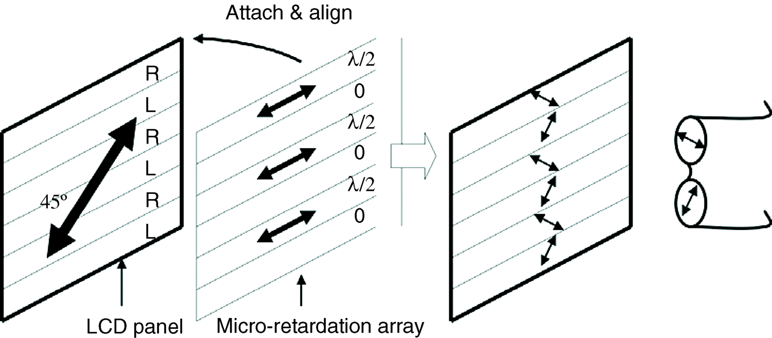
Hence the two planes of the linear polarization are perpendicular and are received by the equally perpendicular polarizing glasses of the viewer, as depicted in Figure 2.1. In this way each eye perceives only the rows labeled R for the right eye and L for the left eye. Only if the planes of polarization are not exactly perpendicular is there a component of the luminance causing crosstalk in the wrong eye. If the viewer's head is tilting sideward the axes of the polarization emitted by the display and the axes of the polarization in the glasses no longer coincide. This also leads to interocular crosstalk. This effect constrains the mobility of the head.
The retardation
(2.1)![]()
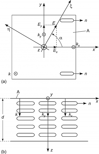
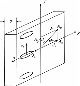
where d is the thickness of the anisotropic layer of the retarder and Δn its optical anisotropy, is caused by the different speeds of the components of the electric field E of light within the retarder sheet. This is shown in Figure 2.2a, where E enters a sheet at an angle α. Within the sheet, the index of refraction is n, with n|| in the x-direction and n⊥ in the y-direction, with Δn = n|| − n⊥. A lengthy calculation determines how the components Ex(t, z) and Ey(t, z) in Figure 2.2a change while they travel in time t in the z-direction through the sheet [2]. The calculation tailored to display applications can be found in [3] on pp. 21–31 and in Appendix 3. The result is
where E0 is the field strength in Figure 2.2, ϕ a fixed phase, and
(2.4)![]()
Ex and Ey can be combined into
with
which is a phase shift, and
and
Figure 2.2 (a) Top view of a retarder and (b) cross-section of the retarder.
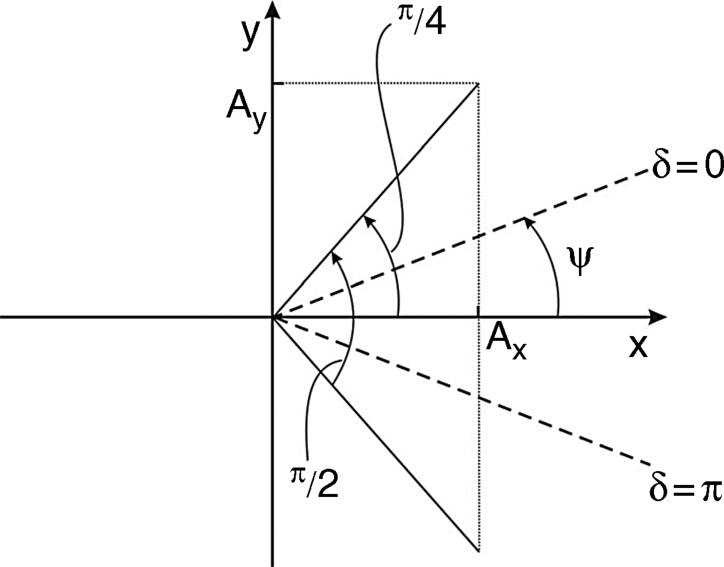
The sum of Ex and Ey for all times t lies in a straight line; the light is linearly polarized and oscillates only in this line. This occurs for
for which Equation 2.5 degenerates into
(2.10)![]()
which is depicted in Figure 2.3 for δ = 0 and δ = π. This figure shows the two planes of polarization. The angle between these two planes becomes π/2 for Ax = Ay, requiring α = π/4 for the incoming light due to Equations 2.7 and (2.8), as indicated by the full lines in Figure 2.3. This demonstrates how linearly polarized light entering a retarder under angle α = π/4, due to Ax = Ay, generates the two perpendicular linearly polarized phases of light required for 3D perceiving glasses. The meanings of the two values for the phase shift δ at the output of the retarder sheet with thickness z0 are derived from Equation 2.6. The value δ = 0 is realized for z = 0, meaning that the linearly polarized light is the input light at angle α. The value δ = π, a phase shift, implies with Equation 2.6a retardation at z = z0 of
Figure 2.3 The linear polarization for δ = 0 and δ = π and the perpendicular polarizations in full lines for Ax = Ay.
The retarder is a λ/2 plate with thickness
This is how the retarder has to be designed. The rows in Figure 2.1 with δ = 0 and α = π/4 do not need a retarder, while the rows with a perpendicular polarization require stripes of retarders with thickness z0 in Equation 2.12.
Later we shall need 3D glasses for use with right- and left-handed circularly polarized light. The retarders required for that can also be derived from Equation 2.5, this time for
and again
Equations 2.13 and 2.14 inserted into Equation 2.5 yield
(2.15)![]()
meaning that
(2.16)![]()
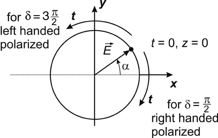
lies on a circle, as shown in Figure 2.4, representing circularly polarized light. Now we investigate the angle ψ of E in Figure 2.4 given by Ex and Ey in Equations 2.2 and 2.3 as
Figure 2.4 The right- and left-handed circularly polarized light in retarders.
with
For t = 0 and z = 0, we obtain Ey(0, 0)/Ex(0, 0) = tan α, as indicated in Figure 2.4. The progress of ψ with time t is provided from Equations 2.17 and 2.18 as
For 0 < δ < π, which includes δ = π/2 needed for Equation 2.13, the progress of ψ with time in Equation 2.19 is for α![]() [0, π/2] negative for all z, as shown in Figure 2.4. This indicates that for δ = π/2 the circularly polarized light is right-handed. For π < δ < 2π, which includes δ = 3π/2 needed for Equation 2.13, the progress of ψ over time is positive, as shown in Figure 2.4. For δ = 3π/2 this indicates that the circularly polarized light is left-handed. Only for δ = π/2 and δ = 3π/2 is the light circularly polarized, which is needed for a backlight with a constant luminance. Equation 2.6 yields the thickness z0 of the retarders for the two δ-values as
[0, π/2] negative for all z, as shown in Figure 2.4. This indicates that for δ = π/2 the circularly polarized light is right-handed. For π < δ < 2π, which includes δ = 3π/2 needed for Equation 2.13, the progress of ψ over time is positive, as shown in Figure 2.4. For δ = 3π/2 this indicates that the circularly polarized light is left-handed. Only for δ = π/2 and δ = 3π/2 is the light circularly polarized, which is needed for a backlight with a constant luminance. Equation 2.6 yields the thickness z0 of the retarders for the two δ-values as
representing right-handed circular polarization
representing left-handed circular polarization.
A further condition for the circular polarization of the retarder is Ax = Ay in Equation 2.14 resulting in α = π/4 in Figure 2.4.
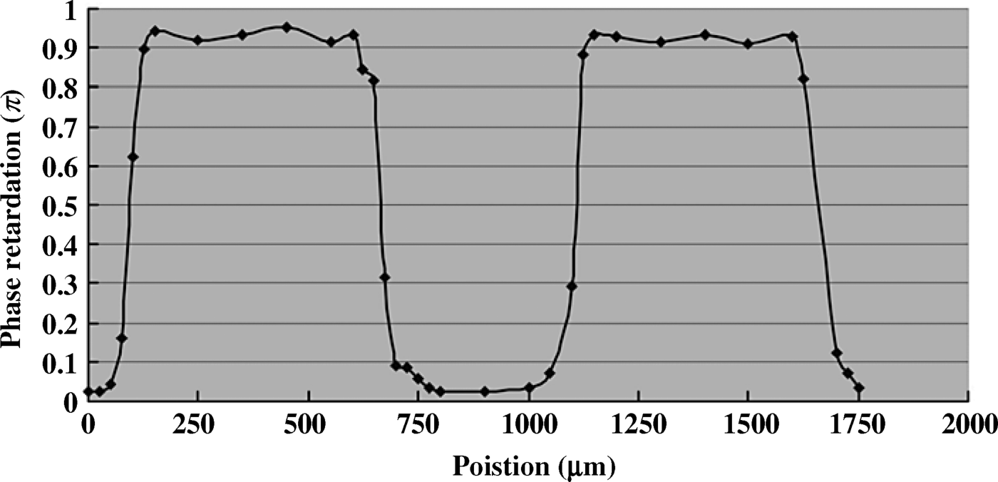
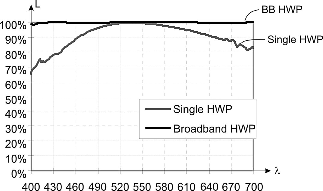
Retarders are preferably realized as in-cell microretarders, which yield a wide viewing angle as they consist of a thin film integrated without a gap into the conventional layers of an LCD [4]. Figure 2.5 shows the layers of an LCD on the color filter side with the in-cell microretarder deposited on top of the in-cell polarizer. The retarder consists of reactive liquid crystal material which can be transformed into a dense film. The polarizer is rubbed in order to unidirectionally tilt the polymer side chains of this material. After deposition by spin coating into a striped mask, the reactive liquid crystal is polymerized and cured by exposure to UV light. Then the mask is removed and the temperature raised to 100 °C, while the reactive liquid crystal is again exposed to UV light. The entire process has to take place in nitrogen, as in oxygen the polymerization is degraded. The phase shift achieved after the treatment in nitrogen is 0.95π, while in oxygen only 0.7π would have been reached. Figure 2.6 demonstrates the rather sharp profile of phase shift obtained, even though the zero phase shift should be somewhat wider [4].
Figure 2.5 The placement of the in-cell microretarder among the layers of the color filter side of an LCD.
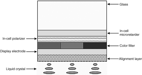
Figure 2.6 The phase retardation across a column of an LCD.
Some of the disadvantages of the linear polarization of the two views can be avoided by circular left- and right-handed polarization of the views as depicted in Figure 2.7 [5]. We know from Equations 2.20b and the associated text that for a retardation of λ/4 the light is right-handed circularly polarized, whereas for a retardation of 3λ/4 it is left-handed. This is used for the two row-wise patterned views in Figure 2.7. The display is fed by a linearly polarized backlight with angle α = π/4, a precondition for the results in Equations 2.20a,b. The first retarder is a λ/2 plate for the first view, while there is no retardation for the second view. The second retarder in Figure 2.7 is a λ/4 plate for both views. The final result is a retardation of λ/2 + λ/4 = 3λ/4 for the first view which, according to Equation 2.21, represents left-handed circularly polarized light, while the second view has a retardation of λ/4 representing, according to Equation 2.20, right-handed circularly polarized light, as shown in Figure 2.7.
Figure 2.7 Stereoscopic display with circular right- and left-handed polarization.
For both eyes the eye glasses contain a λ/4 plate. This adds λ/4 to each retardation yielding 3λ/4 +λ/4 = 2λ for the first view and λ/4 + λ/4 = λ/2 for the second view. From Equations 2.9 and 2.11 and the associated text, this represents perpendicular linear polarizations facing the viewer. This setup is insensitive to tilting of the head, because in each position the glasses encounter the same circularly polarized light. Further, the leakage of light due to imperfect perpendicular polarization in the display itself is also avoided by using circularly polarized light where angles play no role. Finally, the viewing angle in the circular approach is wider than for linear polarization, because the change of retardation with changing viewing angles does not occur for circular polarization. These are striking advantages of circular over linear polarization. However, three retarders are needed instead of only one retarder for linear polarization.
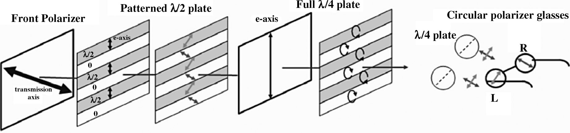
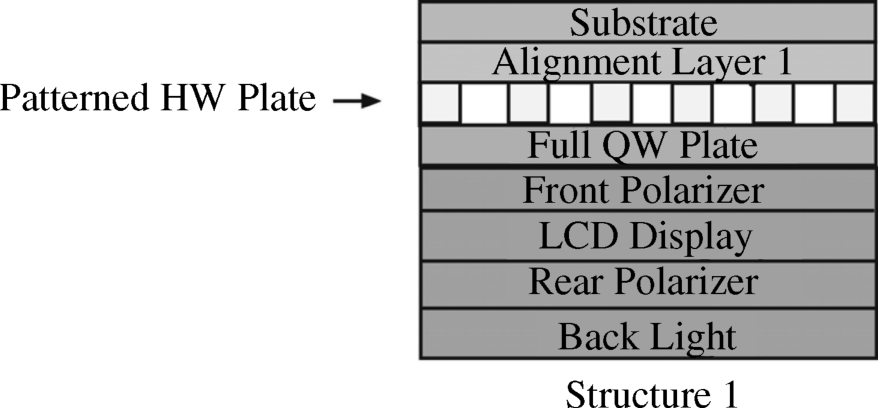
Figure 2.8 depicts the sequence of layers in an LCD with a patterned half-wavelength (HW) plate and a quarter-wavelength (QW) plate. The QW plate can also be placed on top of the front polarizer or between an overcoat alignment layer and the front polarizer. The additional layers certainly add to the thickness d of the arrangement. The larger the value of d, the more stray light may cause crosstalk, as demonstrated in Figure 2.9. Vertical crosstalk can reach 10%. The crosstalk ct as a percentage of the desired luminance is defined by
Figure 2.9 Crosstalk at different viewing angles dependent on the thickness d of the layers.
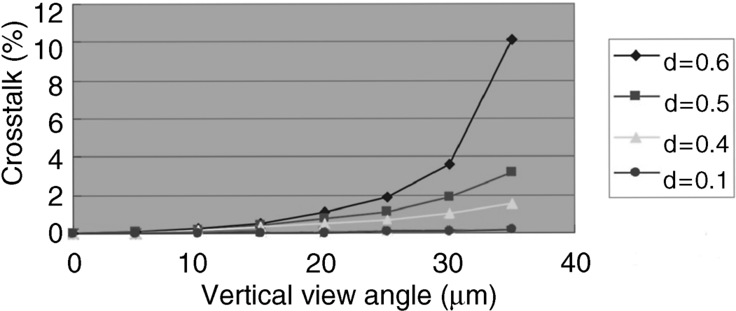
Figure 2.8 The sequence of layers in a display with a HW and a QW plate.
A remedy in [6] against vertical crosstalk is black stripes on the patterned retarders, which are centered around the black matrix of the color filter. These black stripes reduce crosstalk to 1%.
2.1.2 Wire Grid Polarizers for Processing of the Second View
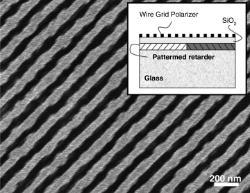
Figure 2.10 depicts a wire grid polarizer (WGP) consisting of a highly conducting grating, for example, out of aluminum, representing the wires [7]. If the conductors belong to an open circuit they reflect the component of the incoming electric field E of the light parallel to the grid, while the component perpendicular to it passes. That way the passing light is linearly polarized perpendicular to the conductors. The grid does not have to be parallel to the edges of the substrate as shown in the scanning electron microscope image in Figure 2.11, where also a typical sequence of layers, namely WGP, SiO2, patterned retarder, and the glass substrate, are indicated. If the conductors were short-circuited the E-components parallel to the conductors would be erased, while a current flows; that way again, only the perpendicular component is preserved. For displays the open circuit is the cheaper solution, being also cheaper than conventional polarizer foils, a retarder, or a polarizing beam splitter (PBS). The pitch p of the grid in Figure 2.10 has to be less than λ and is chosen around 144 nm. The grating is covered by a SiO2 planarization layer, which also permits a dense packing of the layers free of crosstalk creating parallax problems. This ensures a wide viewing angle.
Figure 2.10 A WGP on a glass substrate.
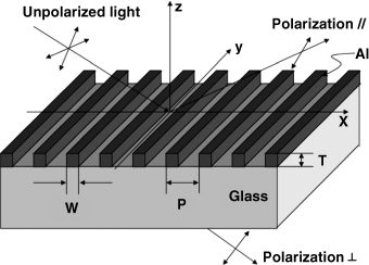
Figure 2.11 SEM image of a WGP slanted with respect to the edges of the substrate.
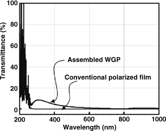
A solution with four WGPs is shown in Figure 2.12 [8]. The patterned left and right eye rows are illuminated by an unpolarized backlight. The odd-numbered rows possess WGP1s for an angle of 45°, while the even-numbered rows have WGP2s for 135°. This light with crossed linear polarizations passes through a regular LCD, a TN cell (twisted nematic cell) or a VA cell (vertically aligned cell), which exhibit a polarizer at the receiving end, for each row rotated by 90°; that is, for the odd rows a WGP3 with 135° and for the even rows a WGP4 with 45°. So each pair of rows represents a TN cell with crossed polarizers. The two polarizations received by the eye glasses are also crossed, as usually done in 3D displays with linear polarizations. The transmittance of a conventional polarizer and of a WGP is compared in Figure 2.13. At short wavelengths the desired zero transmission is reached only by the conventional polarizer.
Figure 2.12 Stereoscopic display with four WGPs.
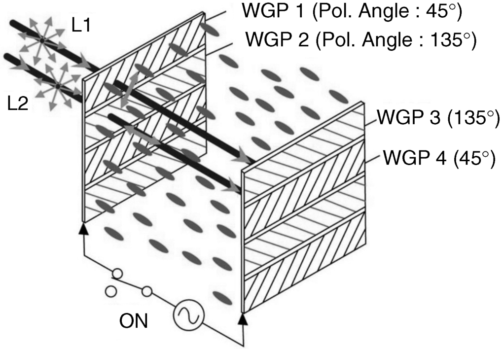
Figure 2.13 Transmittance versus wavelength of a conventional film polarizer and of a WGP.
As the WGPs are placed adjacent to the liquid crystal layer, there is no parallax problem, ensuring a wide viewing angle. As always with linear polarization, tilting of the head leads to a mismatch of the rectangularly polarized light with the crossed polarizers of the lenses.
This is avoided by an approach based again on circularly polarized light using a conventional polarizer, a WGP, and two retarders, with a pitch of 252 μm, the pixel pitch, as shown in Figure 2.14 [7]. The unpolarized backlight passes a conventional 45° polarizer and enters the patterned rows for the two views. After having traveled through an LCD, it passes through a 135° WGP. The light exiting the WGP is 45° off 180° and meets the 45° requirement for light entering retarders to be transferred into right- and left-handed circularly polarized light, as stated in Equations 2.20a,b. From the retarder with retardation λ/4 Equation 2.20 we obtain right-handed circularly polarized light and for the retardation by 3λ/4 Equation 2.21 left-handed circularly polarized light. This light is received by the viewer's eye glasses with right-handed and left-handed circular polarizations.
Figure 2.14 Stereoscopic display with a WGP and two retarders.
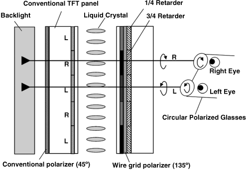
Tilting the head does not degrade the image quality. The WGPs are tightly attached to the color filter and the retarders are close to the liquid crystal layers, avoiding parallax problems.
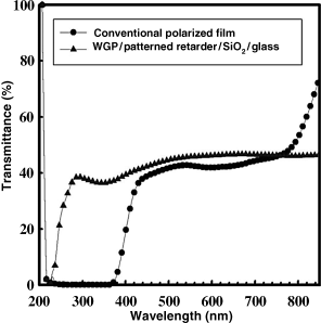
Figure 2.15 compares the transmittances of a conventional polarizer to the packaged WGP/patterned retarder/SiO2/glass layers. The latter works at short wavelengths and provides 45% transmittance instead of 40% with the conventional polarizer.
Figure 2.15 The transmittance of a conventional polarizer and of the combination WGP/patterned retarder/SiO2/glass.
2.1.3 Stereoscopic Display with Two LCDs
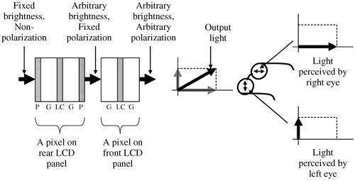
There is a peculiar area multiplex display in which each pixel is used twofold by simultaneously transmitting the luminances and colors for the right eye and the left eye view. That way the full resolution can be assigned to both the left and the right eye [1], but it requires two LCDs, as shown in Figure 2.16. The two LCDs are placed on top of each other. The rear one is fed by an unpolarized backlight which allows to pass through each pixel the root of the sum of the squares of the luminance ll for the left eye and lr for the right eye. The total luminance is
![]()
where k is a factor for the adjustment of lt to the requirements of the display. The total luminance lt passes through a polarizer into the second LCD, which rotates the polarization pixel-wise to such an angle that the component of the luminance parallel to the polarization of the left eye is equal to ![]() . Then the perpendicular component parallel to the perpendicular polarization for the right eye is equal to
. Then the perpendicular component parallel to the perpendicular polarization for the right eye is equal to ![]() . The angle α of the rotation is determined from the components as tan α = ll/lr. A more precise adjustment takes care of the nonlinear relation between the gray shade of the luminance and the voltage across the LCD, which is the curve for the γ-correction [3].
. The angle α of the rotation is determined from the components as tan α = ll/lr. A more precise adjustment takes care of the nonlinear relation between the gray shade of the luminance and the voltage across the LCD, which is the curve for the γ-correction [3].
Figure 2.16 The dual layer stereoscopic LCD.
This ingenious two-LCD approach, also known as dual layer 3D LCD, needs an accurate polarization positioned parallel to the polarization of one eye glass. This requires all pixel-wise rotations of the polarization to be precise. This is not easy to achieve and requires precise pixel voltages.
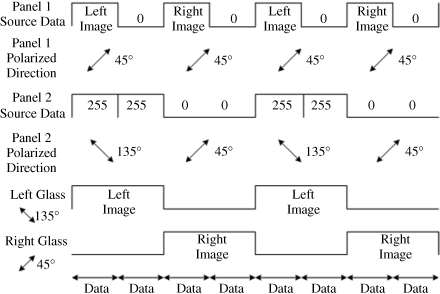
The approach in [9] also uses two displays, called LC panel 1 and LC panel 2 in Figure 2.17. The two views are placed next to each other in the same row separated by a black insertion to limit crosstalk. Use of such an insertion is called dynamic polarization. The processing of the left and right image is shown in Figure 2.18. All images leaving panel 1 have a 45° polarization. Panel 2 changes the left eye image with the black insertion into a 135° polarization which is received by the same polarization in the left eye glass. The 45° polarization of the right image passes panel 2 unchanged and is received by the 45° polarization in the right eye glass. The black insertion in each of the two panels in Figure 2.18 next to the two images limits crosstalk, as there is no leakage of light from the black insertions. This is especially helpful if the light response of a panel is not short enough. This processing is characterized by the use of a linear polarization in the eye glasses.
Figure 2.17 Sequence of layers in a stereoscopic display with two LCDs and dynamic polarization (TFT = Thin Film Transistor).
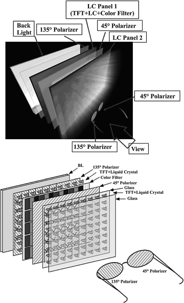
Figure 2.18 Flow chart of dynamic polarization with crossed polarization of the eye glasses.
Another way to create dynamic polarization is shown in Figure 2.19, where shutter glasses are used instead of polarizing glasses. The polarization throughout the processing remains 45°. The left eye glasses exhibit a 45° polarization when the left eye is supposed to perceive its image, whereas they are switched to block the light otherwise. This works, vice versa, for the right eye.
Figure 2.19 Flow chart of dynamic polarization with shutter glasses.
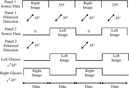
Again black insertions are embedded in all images in order to suppress crosstalk. A shortcoming of the solution in Figure 2.18 is that the right eye image is brighter than the image for the left eye, because panel 2 does not have to be switched, thus avoiding loss of on-time and luminance. Further, there are chromatic aberrations due to scattering of light when neighboring channels switch polarization. All this is avoided in the solution in Figure 2.19 which stays with one polarization. However, it needs the shutter glasses to be switched on and off fast enough.
2.2 Combined Area and Time Division Multiplex for 3D Displays
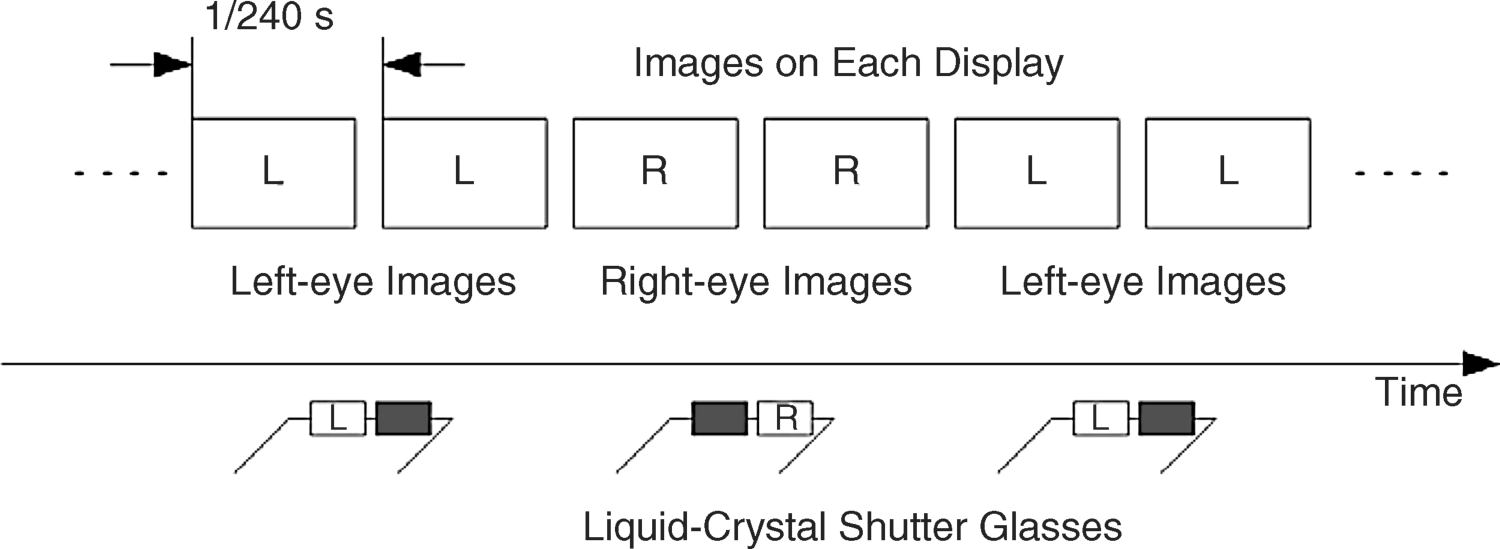
So far we have considered area division in the form of patterned rows separated for the left and the right eye. The images were presented to the viewer simultaneously. The lines had the full resolution of, for example, 1920 columns for FHD TV, but the columns had only half the resolution for each view separately. Now we investigate an approach in which the two views consist of the left and the right half of the TV screen which, for example, for FHD TV possesses 1920 columns and 1080 rows. So the horizontal resolution of the two images is only half the FHD resolution, while in the vertical direction, contrary to the previous solutions, we encounter the full TV resolution. The two images are not presented simultaneously but time sequentially. The viewing is performed with glasses also working time sequentially [10].
The solution to be presented employs a 240 Hz frame rate, excels over a wide viewing angle of 180° by using two subpixels, and masters the high speed required by parallel signal processing [10]. In order to reduce and even suppress motion blur, as demonstrated in Section 1.4, high-quality 3D TV has to use at least 240 Hz frames. Thereby the frame time T is reduced from 16.6 ms for 60 Hz to T = 16.6/4 = 4.1 ms. The row address time Tr = T/n, where n is the number of rows, and shrinks for 1080 rows of FHD TV to Tr = 4.1/1080 ms = 3.79 μs. Figure 2.20 [10] shows the times Tr versus the frame time T for HD with n = 720, FHD with n = 1080, and UD (Ultra Definition) with n = 2160. Before we go into the details, an overview of the problems to be solved for the combined area and time division approach will be given:
1. With present a-Si technology for TFTs the charging of the capacitors in a row in Tr = 3.79 μs is impossible. Therefore a fast charging scheme with parallel processing, in addition to achieving a 180° viewing angle, has to be developed.
2. Video cameras provide the two half images in a 60 Hz frame. For the 240 Hz frame in Figure 2.21 three interpolations from the 60 Hz image have to be derived. The interface between the two half images must be controlled by motion vectors.
3. The two images have to be presented time sequentially.
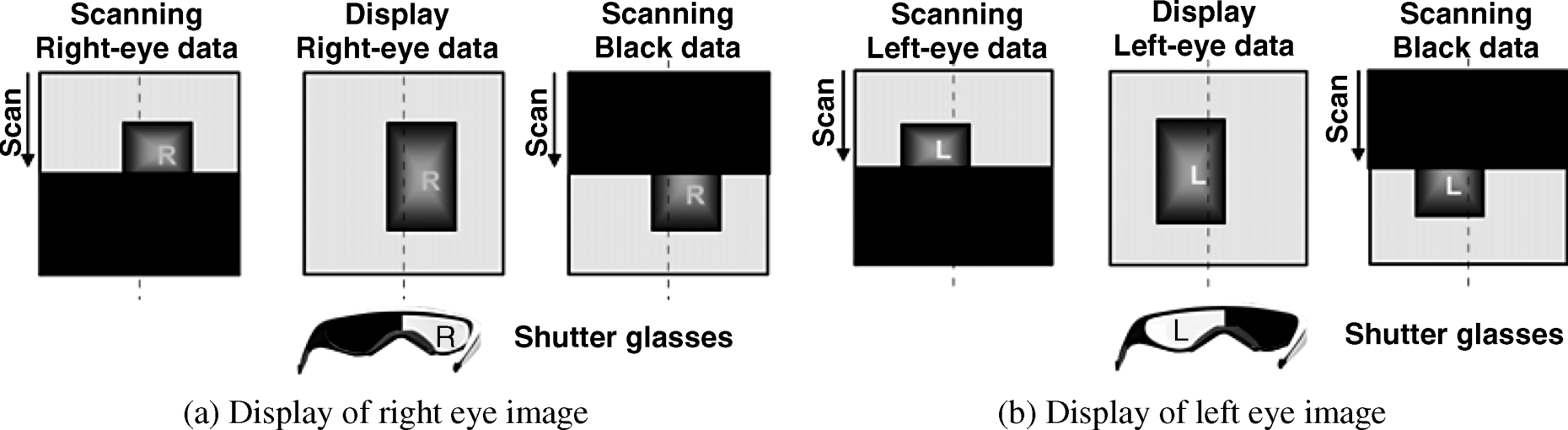
4. The shutter glasses in Figure 2.22 have to receive the images also time sequentially by switching the lens for the right eye transparent for viewing the right image while the left lens is blocked, and vice versa for the left image.
Figure 2.20 Available charging time versus frame rate.
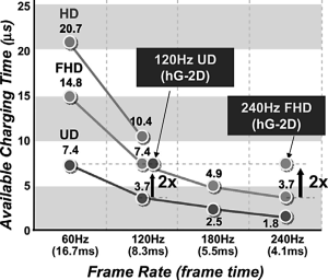
Figure 2.21 The 60 Hz frames with the additional frames for 240 Hz.
Figure 2.22 Time sequential viewing of the two images with shutter glasses.
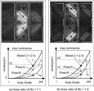
Considering overview point 1, for a 180° viewing angle, necessary for home TV, the required luminance ILC req received by the eye versus the luminance lutin of the picture source with up to 256 gray shades has to meet the physiological law
where γCRT = 2.4 is also called the γ-correction. This is usually met for a vertical view onto the display. In order to realize it up to 180°, we have to satisfy Equation 2.22 also, for example, at 60° and then less accurately around 60° up to 180°. To this end a pixel is subdivided into two subpixels with areas A and B in Figure 2.23a and b and with different voltages VA and VB[10–14]. The subpixels possess the γ-curves γA and γB and the approximate luminances IA ≈ AVA and IB ≈ BVB. The total luminance is It ≈ AVA + BVB, which is supposed to equal ILC req in Equation 2.22. The degrees of freedom to realize this are A, B, VA, and VB which are determined experimentally for all pixels of the display. Examples for the curves γA, γB and γ = γA + γB are depicted underneath the subpixels for different selections of the area ratios A/B. The sum γ in Figure 2.23a and b approximates ILC req for γCRT = 2.4. Obviously γA represents a high γ and γB a low one; hence A is often labeled H for high and B is labeled L for low.
Figure 2.23 The division of a pixel into two subpixels with areas A and B (upper part of figure) and γ-curves for the subpixels with different area ratios (lower part of figure).
The addressing circuit for the subpixel voltages VA and VB is shown in Figure 2.24 [10–12, 14]. Its operation exhibits two steps: the gate voltage Gn activates TFT1 and TFT2 in the subpixels A and B and then the data column charges the capacitors in both subpixels to the same voltage VA.
Figure 2.24 The addressing circuit for the subpixels A and B.
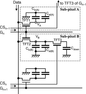
Then the voltage CSn activates TFT3 which allows the capacitors CLC(B) and Cst(B) to be partially discharged onto capacitor Cdown in subpixel B. After that the capacitors in subpixel B exhibit the lower desired voltage VB < VA, necessary for the creation of the two γ-curves γA and γB. This provides the 180° viewing angle of the display.
The capacitor Cdown has the function of charge sharing with the other capacitors. This is why its addressing voltage is called CSn.
Figure 2.25 depicts an array of pixels with the addressing voltages and the time slots in which they work. Each column has two data lines and in each time slot two voltages such as Gn and Gn+1 as well as CSn and CSn+1 are working in parallel signal processing manner. In subpixel H, which stands for A, and subpixel L for B, are their associated TFT1 and TFT2, while TFT3 on the right hand side is connected to Cdown. In the second row the pixel-addressing TFT1 and TFT2 are on the right side and TFT3 and Cdown on the left. This placement continues to alternate. This arrangement allows the simultaneous working of the gate voltages Gn and Gn+1 to charge the capacitors in two pixels in the first two rows by the data lines next to the pixels to the left and to the right. This means that we charge two rows in one time slot of the gate voltage, allowing us to double the time for charging. This is indicated in Figure 2.20, where for FHD TV the time of 3.7 μs for charging one row is doubled to 7.4 μs, thus rendering the charging feasible for a-Si TFTs. This doubling of the time for charging is the advantage of parallel processing. The signal processing is only completed after having performed the charge sharing by activating TFT3 at a later time slot for the voltage CSn. However, this is performed independently without using up time for charging the main pixel capacitors.
Figure 2.25 Array of pixels with the addressing circuit in Figure 2.24.
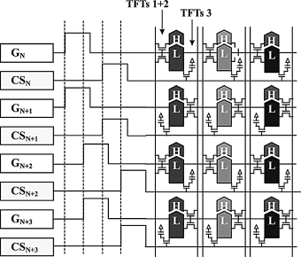
The inventors labeled this addressing scheme the CS-SPVA method, where CS stands for charge sharing and SPVA for super patterned vertically aligned liquid crystal cells.
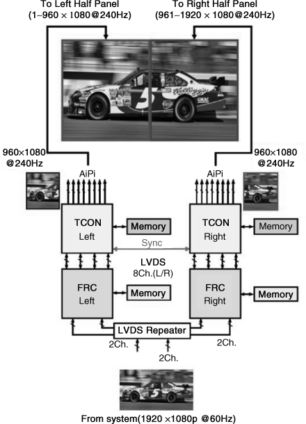
As for overview point 2, the signal representation with 240 Hz frames instead of 60 Hz provided by the TV camera requires additional motion estimation (ME) and motion compensation (MC). For the three 240 Hz interpolations in Figure 2.21, the flow of signals from the input at the bottom with 1980 × 1080 pixels at 60 Hz upwards is shown in Figure 2.26. The left and right halves of the image are processed in parallel. The frame rate converters (FRCs) generate the 240 Hz FHD interpolated stream, where artifacts at the center line of the two images have to be suppressed. For this, motion vector information from the right side is needed by the left side and vice versa. The FRCs are fed by repeaters which twice duplicate the input signal. The results are transmitted to the timing controllers (TCONs) and the LCD panel's column drivers by way of an advanced intrapanel interface (AiPi). The pixel data has 800 Mb/s, which reduces the number of transmission lines required.
Figure 2.26 Transformation of the two 60 Hz images into a frame rate of 240 Hz.
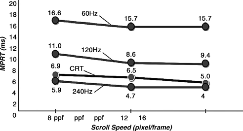
The 240 Hz frame was used to reduce the blurred edge width (BEW) which, according to Section 1.4, is the cause of crosstalk. The degree to which this was achieved is measured by the motion picture response time (MPRT). This is derived from the blurred edge time (BET) associated with the BEW in Figure 1.5b. The BET normalized by the frame time, called the N-BET, is equal to the MPRT. The MPRT also includes the delay by the rotation of the liquid crystal molecules and the holding effect of the LCDs [14], p. 326.
Figure 2.27 shows the MPRT in ms versus the scroll speed, that is, the speed of the addressing of the rows in pixels per frame (ppf), for various frame rates. At a 240 Hz frame rate and a 12 ppf addressing speed, the MPRT was 4.7 ms, an excellent result, even better than the 6.5 ms of a CRT, even though the CRT does not exhibit the holding effect of LCDs. With this result LCDs have finally surpassed the motion picture quality of CRTs.
Figure 2.27 The motion picture response time (MPRT) versus the scroll speed in pixels/frame with the frame rate as parameter.
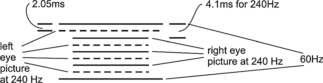
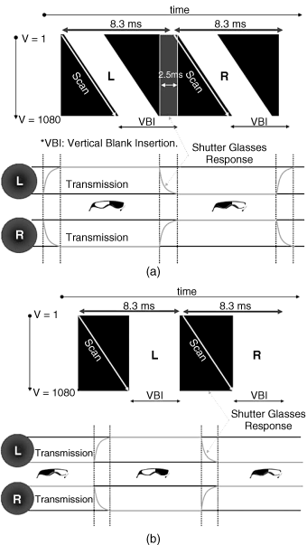
As for points 3 and 4, the images for the left and the right eye are presented by the time sequential driving. The viewer uses shutter glasses providing an on–off operation. This process is shown in Figure 2.22, where the shutter glasses switch as synchronized by the time sequential presentation of the two images as already mentioned in overview point 4. The timing of this switching is not revealed in [9] but could proceed as indicated in Figure 2.28. There the time for the right eye images are drawn in full lines and for the left eye images in dashed lines. These times state when the full image has been completely written into the display. The writing in by scanning the rows starts 4.1 ms earlier. This means that the open shutter receives part of the time overlapping information from both images, which the eyes may tolerate.
Figure 2.28 Timing of the two time sequential images for a 240 Hz frame rate.
The solution in [10] is a candidate for high-quality 3D FHD TV with a higher resolution than the patterned approaches in Section 2.1. It even exhibits a MPRT surpassing that of CRTs. A slight difficulty is the heavier active shutter glasses which contain a battery-operated LCD being switched on and off.
2.3 Stereoscopic Time Sequential Displays
The two views are presented time sequentially. This has the advantage that each view possesses the full resolution of the TV screen. This approach was introduced in [15]. The challenging aspects are the delay in which the full luminance of each view is reached and then again switched off. The first effect diminishes brightness and the latter effect may extend luminance into the next view and hence cause crosstalk. Because of the ensuing fast switching requirements the fast π-cell was used in [15]. In most cases the viewer employs shutter glasses, as we encountered in Section 2.2. Their switching has the same effect on luminance and crosstalk as the time sequential display itself. Some solutions to these problems are described in the following sections.
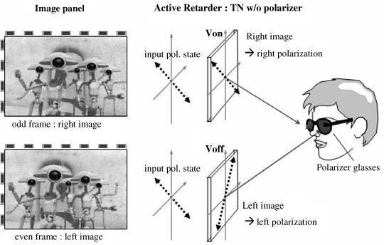
2.3.1 Time Sequential Viewing with an Active Retarder
The concept of this 3D display is shown in Figure 2.29 [16] with the two images, the odd frames for the right eye, and the even frames for the left eye. The retarder is placed in front of the display screen. It does not change the polarization of the image emitted by the display if the voltage Von across the retarder is switched on, but it does change the polarization by 90° if the voltage is off. Hence the retarder is a λ/2 plate, as detailed in Section 2.1. The glasses exhibit crossed polarization. If the odd frame image is emitted and the voltage at the retarder is on, the image passes the retarder without a change of polarization and is able to pass the right eye glass as well, but not the crossed polarization of the left eye glass. On the other hand, if the even frame image is emitted and the voltage at the retarder is off, the polarization changes by 90° and passes the left eye glass only. As the retarder with its voltage, called an active retarder, is attached to the display, and the glasses are not switched, they do not need a voltage supply and are hence called passive glasses. The glasses are lighter and less costly but are sensitive to tilting of the head.
Figure 2.29 Two views of the time sequential display with an active retarder.
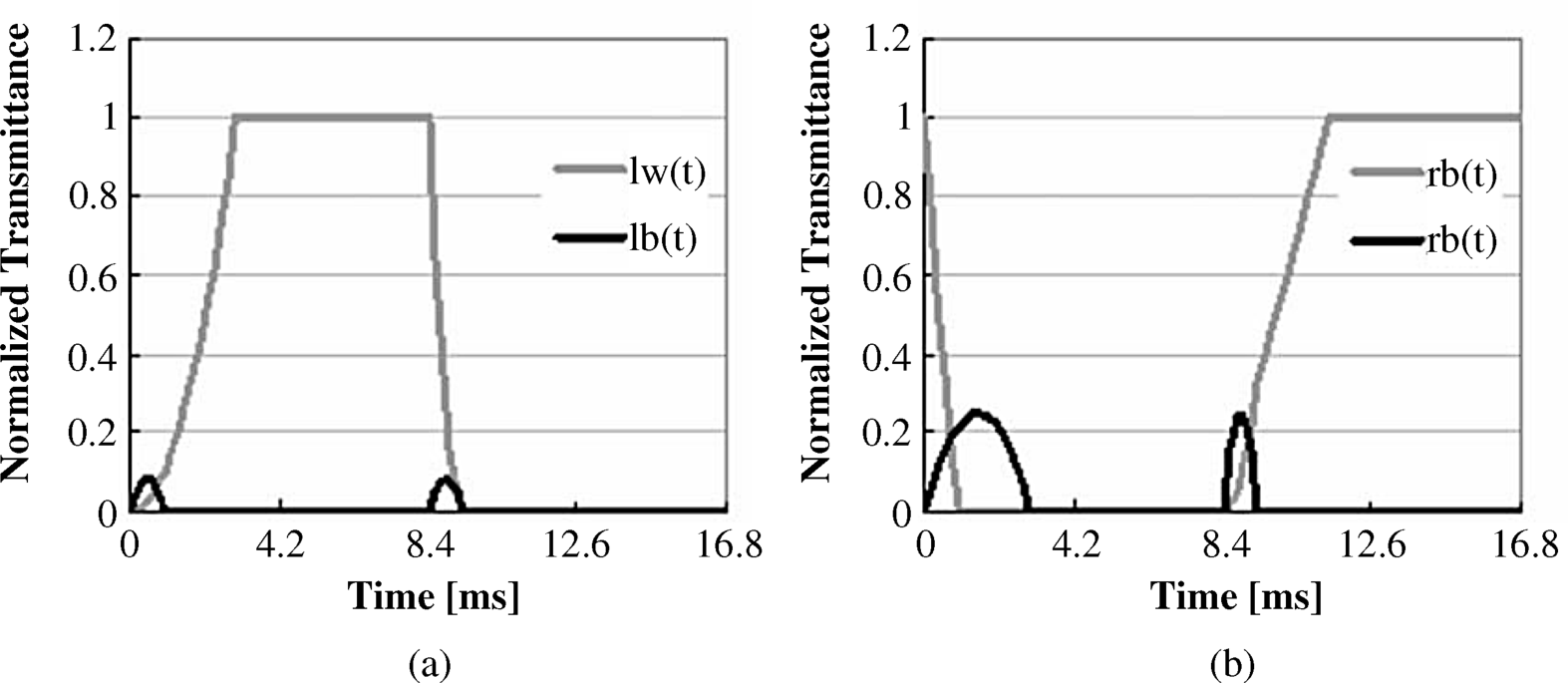
As long as the polarization at the exit of the display and at the eye glasses is perfectly crossed, maximum light is transferred to the viewer. The retarder is thinner than a TN display and hence is exposed to a larger electric field, which accelerates the switching of the retardation. Also, this enhances luminance as the passage of light to the viewer lasts longer. Figure 2.30 depicts a white image ew of the even frame, that is, for the left eye, and a white image ow for the right eye. The rise time of these luminances of 3 ms and the decay of around 1 ms are very small, greatly enhancing luminance. In Figure 2.31a the white color for the left eye together, in bold lines, with the crosstalk from a right eye white is drawn, while in Figure 2.31b the right eye black together, again in bold lines, with the crosstalk from a left eye white to the right eye black is depicted. Further measurements reveal a crosstalk to the left eye of 1.5% and to the right eye of 15.8% which is too high. For the definition of crosstalk Equation 2.21 was used.
Figure 2.30 A white image ew for the left eye and a white image ow for the right eye, both with short response times.
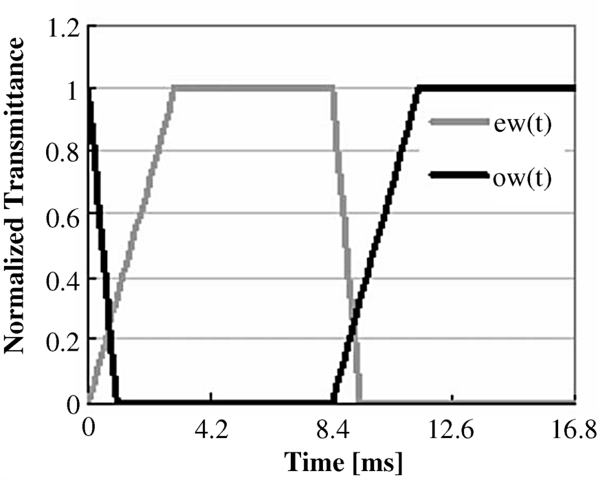
Figure 2.31 Crosstalk in bold lines to a white picture (a) and a black picture (b).
The advantage of this approach for time sequential 3D lies in the method to enhance luminance at full 2D resolution, while crosstalk still requires further attention. The system was extended to circular polarization rendering the passive glasses independent of tilting the head [57].
2.3.2 Fast Time Sequential 3D displays by the use of OCB LCDs
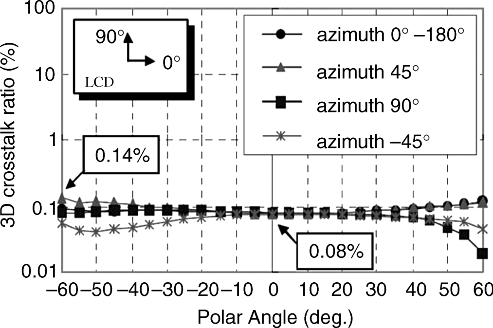
Optically compensated bend (OCB) liquid crystal cells [17, 18] provide a short MPRT of 2.3 ms [18]. The setup of a time sequential system with shutter glasses for the viewer is depicted in Figure 2.32 [19]. Both the display for the sequence of images for the left and right eye and the shutter glasses use the fast OCB cells. A blinking backlight in Figure 2.33 separates the times in which the images are displayed and viewed through the shutter glasses, so leakage of light into the wrong view is strongly shrunk. This manifests itself in a low crosstalk of around 0.1% depending on the polar viewing angle in Figure 2.34. These values are indeed far from pseudoscopy, where crosstalk exceeds 50%, creating a reversal of images, that is, an exchange of the two views. Crosstalk of 0.1% is close to the threshold of visibility [20].
Figure 2.32 The concept of time sequential 3D with OCB cells for the images and the shutter glasses.
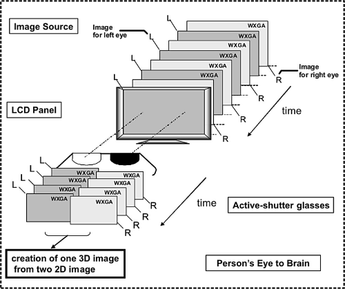
Figure 2.33 Blinking backlights for the images emitted by the OCB cell (upper portion) and the working of the shutter glasses (lower portion).
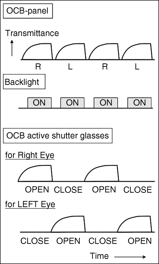
Figure 2.34 Crosstalk in % versus the polar viewing angle for time sequential 3D with OCB cells.
The luminance of the pertinent 2D display is 400 cd/m2. For 3D displays it is of course reduced by the blinking backlight and by the MPRT, even though the OCB cell renders MPRT very short. The 3D luminance is a respectable 120 cd/m2.
2.3.3 Time Sequential 3D displays with black insertions
Black insertions reduce crosstalk similar to blinking backlights. The black insertions will be investigated on the basis of two promising examples.
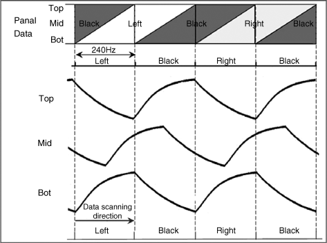
Figure 2.35 [21] shows in the top portion labeled panel data how the rows of the left and right eye images are commonly and time sequentially addressed by scanning from the first row at the bottom to the last one at the top. The same applies for the writing in of the black insertions between the images. Underneath the top, the pertinent waveforms of light over time in the top row, the row in the middle, and the row at the bottom are drawn. To reach a big enough luminance and a small enough crosstalk, one has to consider that luminance does not stop abruptly but decays as a rule in more than a frame time down to zero, and also that black needs more than a frame time to fully develop. Of course, also the location in time and the duration of the on-phase of the shutter influence luminance and crosstalk. Finally the duty cycle of the blinking backlight as a percentage of the frame time is important. All these parameters of backlight and shutter are determined experimentally in order to maximize the luminance of the image while still experiencing a tolerable crosstalk.
Figure 2.35 The scanning of the rows of images and of the black insertion and the pertinent waveforms of light.
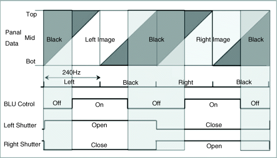
The advantageous location of the blinking backlight unit (BLU) in Figure 2.36 allows most of the luminance of the right and the left image to be transmitted to the viewer. In this example the duration of the backlight is equal to the frame time of 4.1 ms of the 240 Hz frame. The frequency of the backlight is 120 Hz. The left shutter is open as long as the left image is presented, that is, twice the frame time of 4.1 ms. This long time is appropriate for receiving the full luminance of the image, but also entails the danger of picking up stray light which increases crosstalk.
Figure 2.36 A blinking backlight for a time sequential 3D display with a 240 Hz frame rate.
An even larger luminance of the 3D image can be achieved by the scanning backlight in Figure 2.37. This backlight follows the position of the scanned rows such that maximum light is transmitted in spite of its smaller duration. The scanning backlight with the numbered BLUs is centered around the peak of the luminance in each row. The shutter is open during the time of an image and of a black insertion, which is twice the frame time, in order to gather all the light emitted.
Figure 2.37 A scanning backlight for a time sequential 3D display with a 240 Hz frame.
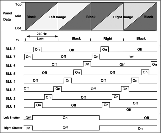
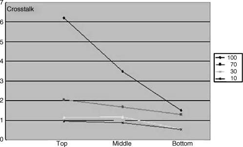
Figure 2.38 shows the crosstalk as a percentage of a blinking backlight versus the positions of top–middle–bottom on the display with duty cycles of 10, 30, 70, and 100% as parameters. The smallest duty cycle has of course the smallest crosstalk of 1%, while the largest duty cycle of 100% leads to the largest crosstalk.
Figure 2.38 Crosstalk for a blinking backlight dependent on the location on the top, in the middle, and at the bottom of an image.
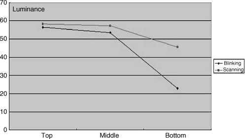
In Figure 2.39 the luminance for a blinking and a scanning backlight is again depicted versus the locations of top–middle–bottom on the display. The duty cycle for both backlights was 50%. Scanning provides of course a larger luminance than blinking. Further, the luminance for scanning is more uniform over the display area.
Figure 2.39 Luminance for a blinking and a scanning backlight with 50% duty cycle dependent on the location on the top, in the middle, and at the bottom of an image.
In order to reach the desired low level of 0.5% crosstalk, faster displays are required. Therefore, using OLEDs for 3D displays is a very attractive idea. The response time of luminance is microseconds and hence virtually negligible versus the milliseconds of LCDs. So for time sequential systems, where fast displays are mandatory, OLEDs are a very attractive alternative.
In [22] OLEDs with black insertions between the two views are used. The rows in Figure 2.3 are scanned from the top downward and exhibit the conventional progressive emission of light, which we have already seen in Figure 2.35. A vertical black insertion separates the left and the right image. The time of 8.3 ms for image and black insertion indicates a 120 Hz frequency for both. The image alone, lasting 4.1 ms, has the property of a 240 Hz frame, where the holding time of the image as in LCDs defines the blur, in this case the very small blur.
Figure 2.40 Conventional scanning of the rows during (a) progressive emission and (b) simultaneous emission.
The viewer uses shutter glasses. This is the conventional approach.
A novel approach is shown in Figure 2.4 where the progressive emission is replaced by the simultaneous emission of all rows. Again, there is a black insertion, also performed by all rows simultaneously. In [22] it is not mentioned how the simultaneous emission of all rows takes place. However, it is stated that the abrupt cessation of the emission is performed by lowering the supply voltage ELVDD in the circuit of Figure 2.41a and 2.41b such that
where Vth is the threshold voltage of the OLED and ELVSS the voltage at its cathode. Inequality 2.23 ensures that the OLED and hence the emission of light are blocked. As OLEDs are very fast this happens in microseconds or virtually abruptly. The simultaneous emission of all rows may be prepared by charging the capacitors Cst in the circuit diagrams of Figure 2.41a and 2.41b by scanning the rows during the black period, while the OLED and hence the light emission are still blocked according to (2.23). Then the voltage ELVDD is raised to render the voltage difference in 2.23 larger than Vth, which abruptly drives the entire OLED into emission, as shown in Figure 2.4. The charging of the capacitors Cst defining the luminance of the pixels can be sped up by the parallel processing in Figures 2.24 and 2.25. The subpixels for enhancing the viewing angle are, however, not needed, as OLEDs already exhibit a wide viewing angle on their own.
Figure 2.41 (a) The conventional six TFTs and one C addressing circuit for OLEDs and (b) the novel three TFTs and one C addressing circuit for OLEDs.
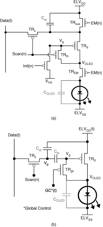
This new OLED development renders insignificant both the time needed for scanning the rows and the response time of the display, thus providing the fastest solution so far. Inventors call this new process the simultaneous emission with active voltage (SEAV) control.
The shutter glasses exhibit a response time of 2.5 ms; however, this time is placed into the black insertions and hence does not decrease luminance. The larger the frame rate, the smaller the crosstalk stemming from motion blur. A small motion blur allows an increase in the duty cycle of the emission, as a percentage of the frame time. This enhances luminance. Figure 2.42 depicts the allowable duty cycle versus the frame rate for progressive emission (PE) and for simultaneous emission (SE). The allowable duty cycle in the SE mode is always larger than in the PE mode, because in the PE mode the turning on of all rows consumes the entire frame time and full hiding of the response time of 2.5 ms of the shutter in each row is virtually impossible. Therefore at 240 Hz the SE mode allows a duty cycle of 50% in Figure 2.42 and the PE mode only 20%.
Figure 2.42 Allowable duty cycle versus frame rate for progressive and simultaneous emission.
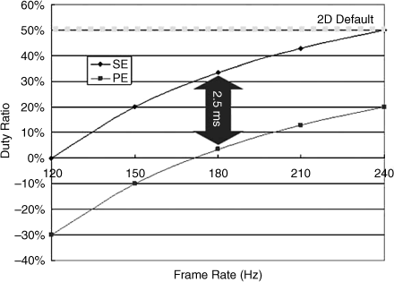
Assuming that the default mode for 2D displays has a 50% duty cycle, then 2D and 3D exhibit the same luminance. At 50% duty cycle the OLED current can be increased by a factor of two and the power consumption is still the same as for conventional operation with a 100% duty cycle; that means with the OLED power on permanently.
The active voltage control in the addressing circuit in Figure 2.41b no longer requires the TFT TRSUS in Figure 2.41a which adjusted the power supply. Employing the active voltage control not only in the data scan step and the emission step, but also in the reset and the Vth storage step, saves three TFTs altogether, reducing the TFT count in the simplified circuit in Figure 2.41b to three TFTs. Further for a 30 in FHD AMOLED (Active Matrix Organic Light-Emitting Diode) panel the capacitance in a pixel can be reduced from 165fF to 85 fF.
For time sequential 3D displays, where speed is of the utmost importance, AMOLEDs with the novel simultaneous emission are likely to play an eminent role due to the inherent switching speed of OLEDs and virtually crosstalk-free operation combined with the wide viewing angle of OLEDs.
2.4 Special Solutions for Stereoscopic Displays
This section focuses on three special solutions: the enhancement of the depth sensation by the control of contrast, the suppression of crosstalk by an algorithm implemented in the display, and the generation of the two images required for 3D by wavelength multiplex.
Subjectively enhanced perception of depth can be achieved by binocular and monocular cues. Binocular cues enhance disparity which, if performed excessively, induces visual fatigue and even sickness [23]. Monocular depth cues appear to be more promising [24]. These cues consist of aerial perception, shading, occlusion, and the relationship between contrast and subjective depth. The higher the contrast between an object and its background in an image, the nearer the object seems to be, whereas the smaller the contrast, the farther away the object seems to be located. This is a monocular psychological effect. The control of contrast can be applied to arouse an enhanced 3D sensation [25].
In order to demonstrate how well this effect works, an experiment was conducted which used two displays in Figure 2.43, one for the left eye and one for the right eye. One display showed the conventional image and the other the contrast-controlled image. Presenting these images alternately allowed the viewers to detect the differences. Each image had a frame frequency of 240 Hz. The left and right eye images were presented frame sequentially with a frequency of 120 Hz. The viewers' shutter glasses operated at 60 Hz.
Figure 2.43 The sequence of stereoscopic images for the investigation of depth controlled by contrast.
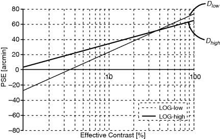
For the quantified monocular depth cue an approximation of perceived depth was derived depending on the spatial frequencies in an image. For low spatial frequencies below 2 cycles per frame time the perceived subjective depth Dlow is given in Equation 2.24; the perceived depth Dhigh in Equation 2.25 belongs to the high spatial frequencies above 2 cycles per frame time. They are
where Ceff is the effective contrast given as
(2.26)![]()
The curves for Dlow and Dhigh depending on log Ceff are plotted in Figure 2.44 with Ceff as abscissa and the so-called point of subjective equality (PSE), meaning the subjective depth in arcmin, as ordinate. Positive values indicate that the objects seem to be nearer, while negative values indicate they appear farther. Nearer signifies a larger disparity and farther a smaller one.
Figure 2.44 The depths Dlow and Dhigh in arcmin versus the effective contrast Ceff in Equations 2.24 and (2.25).
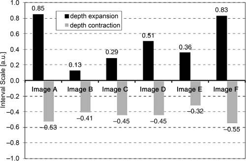
The signal processing required to determine the subjective depths Dlow and Dhigh is depicted in Figure 2.45. The luminance has to be determined because it is needed for the calculation of the effective contrast. For the application of Equations 2.24 and 2.25 the spatial frequencies are needed. The conventional depth Dp has to be estimated. Then the calculation of the factor needed to enhance Dp to Dlow (modulation gain) can take place, upon which the factor is applied to the conventional image providing a new image with an enhanced 3D sensation. How well this works is checked for the six given test images in Figure 2.46. The result is evaluated by test persons and is plotted in Figure 2.47 for the test images A through F. The positive values of the ordinate stand for the expansion of the depth in the images and the negative values indicate a contraction. Therefore the highest and the lowest values at the ordinate signify by how much the interval of depths perceived by the viewers has been enlarged. The results reveal that all images except image B experienced a significant expansion of the depth interval in comparison to the original images. This demonstrates that the algorithm is very successful.
Figure 2.45 Block diagram of the image processing for obtaining the subjective depths.
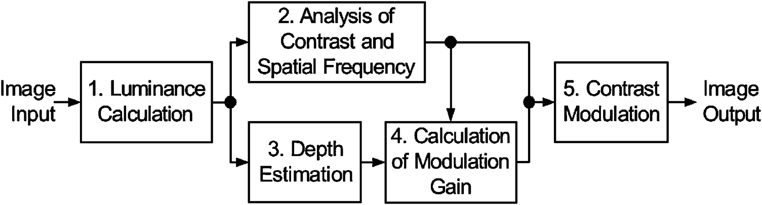
Figure 2.46 Six test images for evaluation of the contrast control.
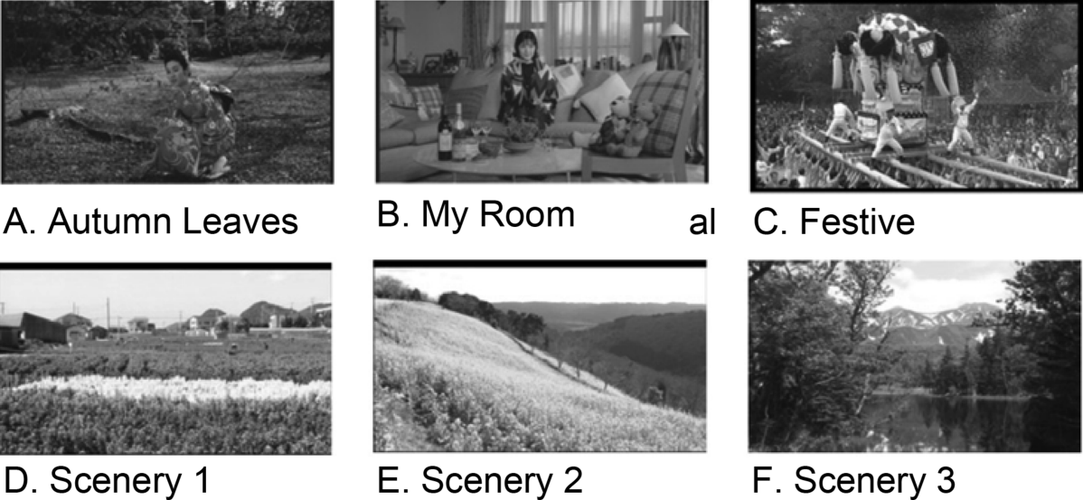
Figure 2.47 The expansion and contraction of the depths perceived by viewers at the six test images in Figure 2.46.
Crosstalk can be reduced by a digital image processing algorithm [26]. For a two-image system, R for the right eye and L for the left eye, the luminances can be expressed by
(2.27)![]()
and
(2.28)![]()
where Ri and Li are the desired luminances provided by the screen for the right and the left eye, while Ro and Lo are the luminances in the image with the crosstalk defined by the factors a and b with the values a,b![]() [0, 1] describing the level of the crosstalk.
[0, 1] describing the level of the crosstalk.
The input signals Ri and Li have to be transformed into new input signals
and
in order to obtain the new output signal ![]() , which is the unadulterated output signal before crosstalk has deteriorated it. As proof we calculate the new output signal
, which is the unadulterated output signal before crosstalk has deteriorated it. As proof we calculate the new output signal ![]() as
as
The same applies to ![]() yielding
yielding ![]() .
.
For the implementation of the algorithm one has to measure the factors a and b in order to calculate ![]() and
and ![]() in Equations (2.29a) and (2.29b). This provides the new input signals from which, according to Equation 2.30, the theoretically crosstalk-free signal
in Equations (2.29a) and (2.29b). This provides the new input signals from which, according to Equation 2.30, the theoretically crosstalk-free signal ![]() and similarly also
and similarly also ![]() are obtained. So Equations 2.29a,b and 2.30 represent the signal processing required to remove crosstalk.
are obtained. So Equations 2.29a,b and 2.30 represent the signal processing required to remove crosstalk.
This crosstalk reduction method assumes that crosstalk over the entire area of the display can be characterized by one factor. If crosstalk affects different areas differently, several factors may be necessary. This is also the case if crosstalk depends on varying parameters such as viewing angle. Then a reduction to low enough values cannot always be expected.
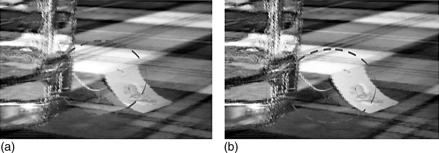
An example is the reduction of crosstalk for the color R in Figure 2.48 from the large value of 16% to below 4% over the entire viewing range from −30° to +30°. The improvement in the image quality by crosstalk reduction is also illustrated by Figure 2.49b with cross talk reduction versus Figure 2.49a without it. The same algorithm has been extended to multiview displays [26] and can of course be used for any 3D system. The algorithm is worth being advanced further.
Figure 2.48 Crosstalk reduction over the entire viewing range for the color R.
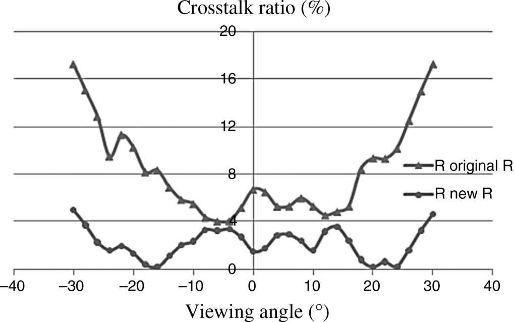
Figure 2.49 (a) Figure without and (b) figure with digital crosstalk reduction.
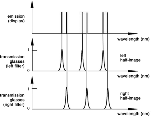
Instead of area multiplex or time multiplex, also wavelength multiplex can be applied for the two images needed for 3D [27–29]. It benefits from the fact that the human retina exhibits three receptors with peak sensitivities for the three primary colors R, G, B as depicted versus wavelength in Figure 2.50. Two triplets of wavelengths, all of them located around R, G, and B in Figure 2.51, are selected to create the two images, one triplet for the left eye and one triplet for the right eye. The two triplets are shifted in wavelength with respect to each other in order to exhibit a minimal overlap.
Figure 2.50 Sensitivity of the receptors in the retina versus wavelength for the three primary colors R, G, and B.
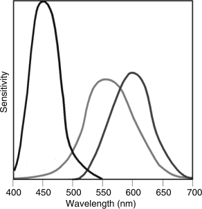
Figure 2.51 The two triples of wavelengths for the two images required for the 3D wavelength multiplex.
This setup represents a recent development based on the anaglyph approach where the two wavelengths for red and cyan, the complementary color to red, were applied.
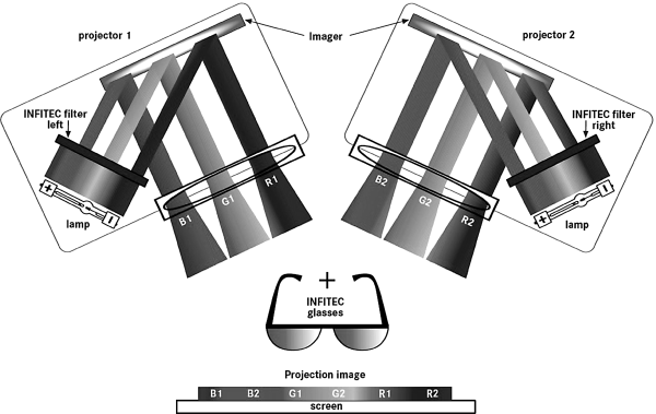
The projector in Figure 2.52 using the two color triples contains two lamps as light sources which emit the three colors after having passed three optical interference filters working as narrow high-Q bandpasses. These bandpasses, as a rule, consist of a sequence of layers with different anisotropic dielectric properties.
Figure 2.52 The 3D projector based on wavelength multiplex.
There is a similarity to the multilayer broadband retarders in Figure 2.61. This similarity also extends to the design method described for Figure 2.61 even though the anisotropic refractive index properties are replaced by the anisotropic dielectric features.
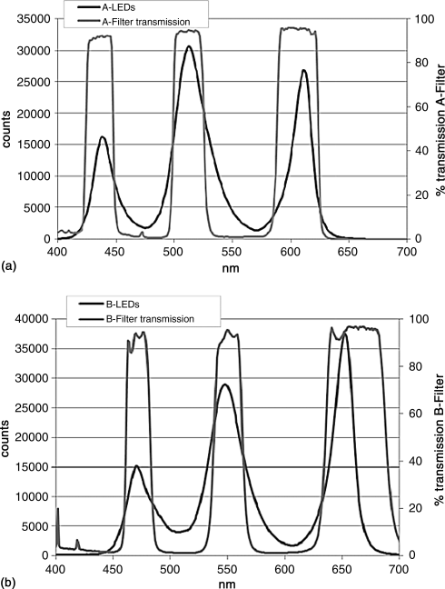
The narrowband color beams in Figure 2.53 are reflected from two displays carrying the left eye and the right eye images. This reflectance is controlled pixel-wise by a voltage. The displays exhibit the full resolution of the image source; however, this requires two displays, contrary to one display with half the resolution. The eye glasses of the viewer possess the same interference filters as the lamps, one for the left and one for the right eye. For the viewer colors for the two images are placed next to each other, meaning that the blue B1 in Figure 2.52 of the first image lies next to the blue B2 of the second image and likewise for green and red.
Figure 2.53 LED emissions spectra and the bandpass transmission curves (a) for the first image and (b) for the second image needed for 3D.
Stereoacuity, the ability to distinguish between two spatial frequencies, decreases with decreasing spatial frequency. On the other hand, very small disparities of only 20 arcsec can still be distinguished by a low modulation of the temporal frequency. This can render the perceived resolution of a 3D display larger than that of a 2D display.
The channel separation between the same neighboring colors for the two images determines the binocular crosstalk. Figure 2.53a and 2.53b depicts the spectrum of an LED backlight together with the bandpass transmission curves of the three colors for one eye (a) and for the other eye (b). At the overlap of the same colors for the two images crosstalk is a maximum but has not exceeded the benchmark value of 1%, while in other areas it is below 0.1%. These remarkable values are due to the steep cut-off characteristics of the filters at perpendicular view onto the display. At oblique viewing angles the dielectric anisotropy shifts the transmission bands toward the blue wavelength. This shift turns out to be less than 2.5 nm if the incidence angle is limited to ±10°, a rather low value for direct view. In order to decrease the shift, a condenser lens was placed onto a tapered tube on top of the LED source.
The narrow bandwidth of the filters diminishes the luminance of the image. Further, to limit crosstalk, the backlight LEDs were turned on only after completion of the image switching, further decreasing the luminance to finally 10 cd/m2.
A good uniformity of luminance can be achieved with regular white screens as the spectral composition of the scattered light is preserved. Thus highly scattering screens with unit gain can be used.
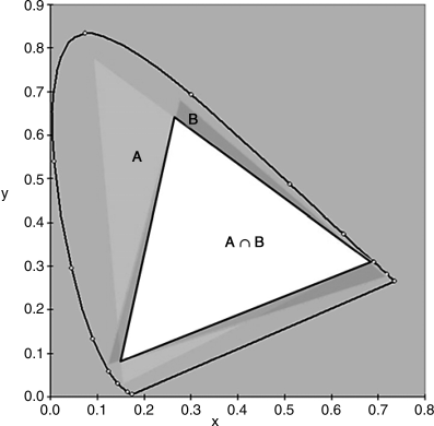
The color gamuts for the primary colors of the two images denominated A and B in the chromaticity diagram of Figure 2.54 are, as a rule, not identical. The eye perceives a 3D image only in the area A ∩ B, where both images are present.
Figure 2.54 The color gamut for the images A and B and the gamut A ∩ B for 3D perception.
Projectors provide the two images required for 3D vision either with different polarizations in an area multiplex mode or in a time sequential mode. For area multiplex the viewer needs polarizing glasses, while time multiplex requires shutter glasses. Polarizing glasses work without a battery, in a passive fashion, whereas shutter glasses need an energy source to switch the glasses on and off. A third approach is wavelength multiplex as already presented at the end of Section 2.4.
The development started with two projectors and two lenses for the two images and resulted in one projector and one lens for both images [30, 31]. For handling the polarizations, a polarizing beam splitter (PBS) or a wire grid polarizer (WGP) is used. As their properties are essential for projectors they are briefly presented here.
The McNeille PBS in Figure 2.55a and 2.55b is a cube of transparent materials 1 and 2 with velocity of light c1 and c2. The polarized light enters the cube in a plane parallel to the surface of the cube. It is composed of two crossed components both perpendicular to the direction of the light as shown in Figure 2.55a and 2.55b. One component is reflected and the other allowed to pass at the plane separating the two materials. The reflected and the passing beam are only crossed polarized if the angle of incidence onto the plane separating the materials is αp, the Brewster angle, with
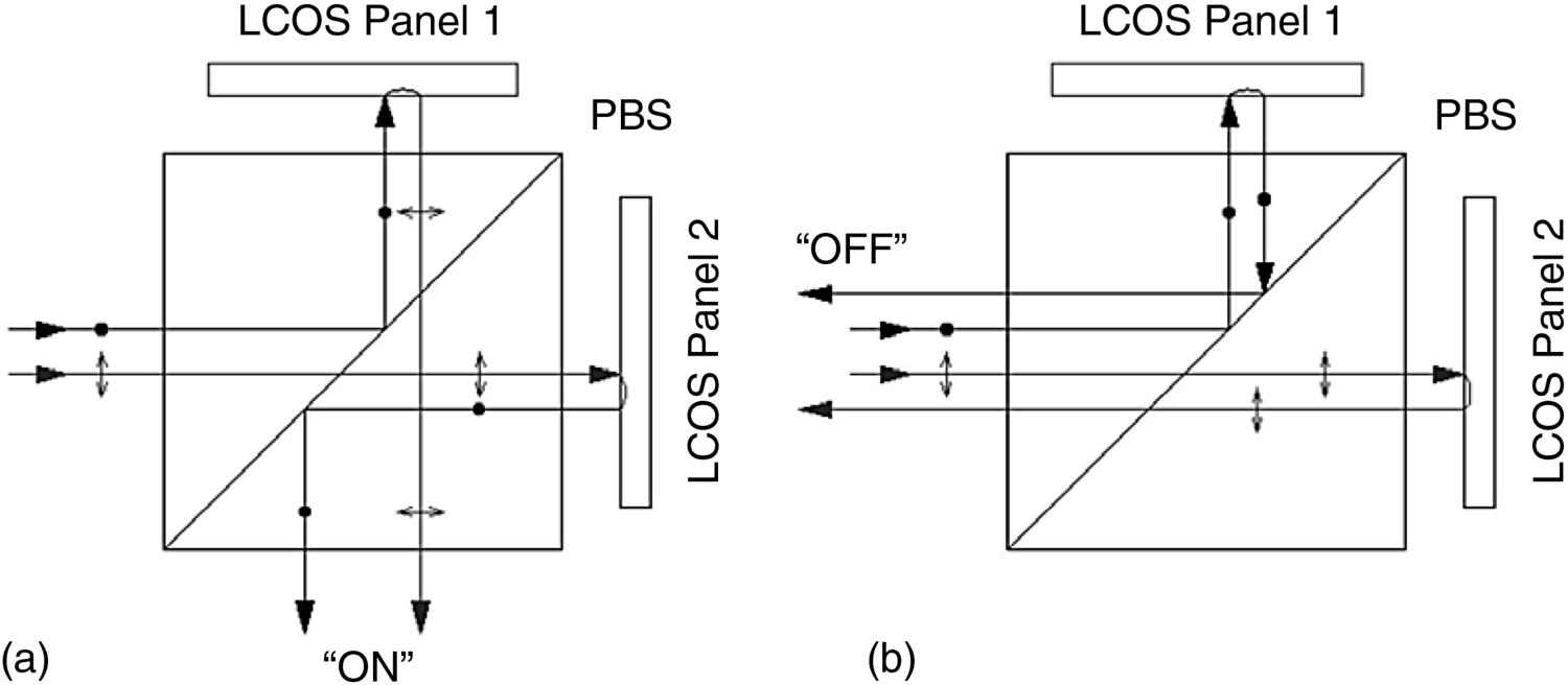
Figure 2.55 The PBS for a simple lens stereoscopic projector (a) for LCOS panels “on” and (b) for LCOS panels “off.”
A sensitive point is the rotation of the cube around any axis, for example, around the vertical axis of the PBS, resulting in a skew ray which violates Equation 2.31 and thus adds an additional component to the prevailing components in each branch of the PBS. This leads to a geometric depolarization [32, 33]. This can be compensated by an O-plate, which is a retardation plate correcting the undesired phase shift.
The advantages of a McNeille PBS are planar transmitted and reflected wave fronts, a short optical pathlength due to a large refractive index of the glass body, no astigmatism, and no multiple reflections that form ghost images. Disadvantages besides the skew ray and its geometric depolarization are the weight and size stemming from the glass body as well as poor contrast and crosstalk depending on residual and thermally induced birefringence of the PBS glass [34].
The WGP, as presented in Figure 2.10 and the surrounding text, is a thin plate and not a more voluminous cube. A geometric depolarization cannot occur, as the light with an E-vector perpendicular to the conductors, the wires, always passes perpendicularly polarized through the conductors, while light parallel to the conductors is reflected as light polarized parallel to the conductors. This is independent of the rotation of the wires toward the incoming light. This is a big advantage over the PBS. A more demanding task is the patterning of the conductors in the nanometer range.
Figure 2.55a and 2.55b depicts the core elements for stereoscopic projection with one projector, one McNeille PBS, two LCOS (Liquid Crystals On Silicon) devices, and a single lens [35]. The polarized incoming light on the left side in Figure 2.55a consists of a perpendicularly polarized p-wave and the crossed polarized s-wave. The s-wave is reflected onto LCOS1 and the p-wave passes to LCOS2. At the two LCOS devices their luminances are modulated by a conventional reflective LCD. The pixels of these LCDs carry the voltages belonging to the desired gray shades. The LCDs act as QW plates rotating the polarization by π/2. So the p-wave becomes an s-wave and the s-wave a p-wave. The p-wave exiting LCOS1 passes the PBS, while the s-wave exiting LCOS2 is reflected and then leaves the PBS parallel to the p-wave. Thus both waves are combined again and can pass a single lens at the exit of the projector which is not shown in Figure 2.55a. This lens magnifies the image of the small LCOS devices to the desired size.
If the voltages across the LCOS pixels are off in Figure 2.55b, the LCOS devices are no longer QW plates and just reflect the incoming waves with an unchanged polarization. This leads to light reflected back into the light source and the image output is black as desired.
Full color is achieved by using time sequential LCOS panels together with a color wheel or pulsed RGB LEDs or lasers. Alternatively, LCOS panels with color filters can be fed by a white light source providing all colors simultaneously, but reducing resolution by a factor of three. The projector is switchable from 3D to 2D by applying two identical 2D images to the p- and s-waves. In the 3D mode viewers have to wear glasses with crossed polarization, which means the glasses are passive.
Instead of LCOS devices, conventional LCDs can be used. They are, however, larger resulting in more bulky projectors and in the need for an increased lens aperture [36]. The images possess the full resolution of the LCOS devices, but luminance of one view is halved when splitting it into the s- and p-waves. Since only one PBS is used, the projector still has a quite high luminance of 42 lm.
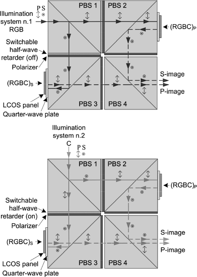
A second 3D projector realizes a high color gamut with two color inputs, one based on an LED primary color RGB triple [37–39], and a second input with the complementary triple amber, cyan C and deep-blue D. Amber replaces yellow which was found not to contribute noticeably to the gamut in Figure 2.56. In this figure the LED RGB triple exceeds the ITU BT 709 norm [40] by 60%; the complementary triple of amber for Y, C, and D enlarges the gamut by another 10%. The six-color system is denominated RYGCBD in Figure 2.56. The spectra of the six colors are shown in Figure 2.57. Those spectra of the two separate systems RGB and YCD overlap partially. In order to control their individual contributions they are kept separate, resulting in two color inputs to the quadruple of PBSs in Figure 2.58 [40]. The input of the RGB triple on the left, shown in the upper cube, and the input of the YCD system on top, shown in the lower cube, are active time sequentially at the same cube. Further investigations revealed that the complementary triple can be replaced. by C alone with no visible degradation of color performance. The function of the PBSs is the same as explained for Figure 2.55a and 2.55b. For the RGB input the QW plate retarders between PBS1 and PBS2 as well as PBS1 and PBS3 are switched off. The luminance-modulated output consists of the s-image and the p-image at the right side. For the C input the QW plate retarders are on and produce a phase shift of π/2 in the polarization. This results in a rotation of the polarization by π/2 transforming the s-wave into a p-wave and the p-wave into an s-wave. This arrangement allows also the modulation of C to exit at the same place as the RGB triple. By using the QW plate the optical path for the color C becomes the same as for RGB. The QW plate can also enhance the light output [41]. Instead of PBSs made out of glass, WGPs were finally used, which in addition to their advantages mentioned above also provided a more homogeneous luminous output.
Figure 2.56 The color gamut of an RGB triple and its extension by the complementary colors Y, cyan C, and deep blue D.
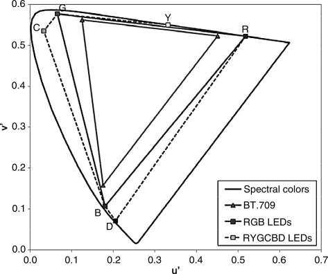
Figure 2.57 LED spectra of R, G, B, Y, C, and D.
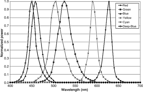
Figure 2.58 A quadruple of PBSs for a R, G, B, and C color display with two color inputs and one lens at the output.
Besides the enhanced color gamut, the projector with four WGPs, two LCOS devices, two QW plate retarders, and two LED light sources possesses in both modulation paths a 10% optical throughput and a very good 20% efficiency of the total light output with an estimated flux of 374 lm for red, 950 lm for green, and 80 lm for blue. These values may even be enhanced by a better match between system and LED étendue. Crosstalk is only 0.5%. The measured values for gamut are for RGB 50% larger and with added cyan 60% larger than the ITU BT 709 norm. This is 10% smaller than the simulated values in Figure 2.56. Both stereoscopic images have a contrast of 1000:1. They reached the high value by applying pretilt compensation. Without it the contrast would have been only 60:1.
The solution for a stereoscopic projector such as in Figure 2.58 and other approaches require broadband retarders (BBRs) working properly in the entire range of visible light with wavelengths from 400 to 700 nm. As the refractive indices n|| and n⊥ are dependent on wavelength, one cannot expect that the properties of the retarders will be independent of λ. Therefore a compensation of the λ-dependency is needed. A solution for this [42] is based on the Jones vectors and Jones matrices, but first we have to introduce the Jones calculus [43]. This calculus is also presented in [3], pp. 21–31 and 85–98, in [43, 44], and in [45], pp. 30–33 and 103–138. The Jones calculus presented only deals with polarized light.
We start with Equations 2.2 and 2.3 for the components Ex and Ey of the electric field strength E of linearly polarized light. The phase in Ey is
![]()
Only δ determines the polarization properties as we know from the text surrounding Equations 2.2 and (2.3). Therefore we set ![]() providing
providing
(2.32)![]()
and
(2.33)![]()
with
(2.34)![]()
which has already been introduced in Equation 2.6. The transformation of Ex and Ey into a complex form yields the Jones vectors Jx and Jy as
and
(2.35b)![]()
from which Ex and Ey follow by taking the real part, an approach common in electrical engineering, known there as calculation with phasors.
The phase difference δ is called the phase retardation, while the retardation itself was introduced in Equation 2.11 as
(2.36)![]()
The speed of the phases in δ is v|| = c/n|| and v⊥ = c/n⊥ with c the speed of light in vacuum. As n|| > n⊥, the speed of the phase related to n|| is slower than the one related to n⊥. Thus the portion of Jy
(2.37a)![]()
represents a slow Jones vector [43, 44] while
(2.37b)![]()
stands for a fast Jones vector in
(2.37c)![]()
The term obtained from Equations 2.35a,b
characterizes the polarization where the factor E0 standing for the luminance is not needed. From Equation 2.38 the Jones vector Jp can be derived as
We know already that for δ = 0, π we obtain linear polarization. The pertinent Jones vector is
(2.40)![]()
where the – sign belongs to δ = π. The phase α = π/4 yields
(2.41)![]()
We know that for δ =± π/2 we obtain polarized light that is left-handed for the + sign and right-handed for the − sign with the Jones vector
(2.42)![]()
which is circularly polarized for α = π/4 yielding
(2.43)![]()
If linearly polarized light with the Jones vector
in the xy-coordinates in Figure 2.59 is applied at the input of a liquid crystal (LC) retarder plate with the axes Js and Jf of the LC molecules lying in the xy-coordinates, we know already that the output is polarized light with the Jones vector Jp in Equation 2.39. As we shall later need luminance, the luminance factor E0 is reintroduced here. The matrix equation describing the input–output relation is
where
is the transmission matrix. The validity of Equation 2.45a is easily confirmed.
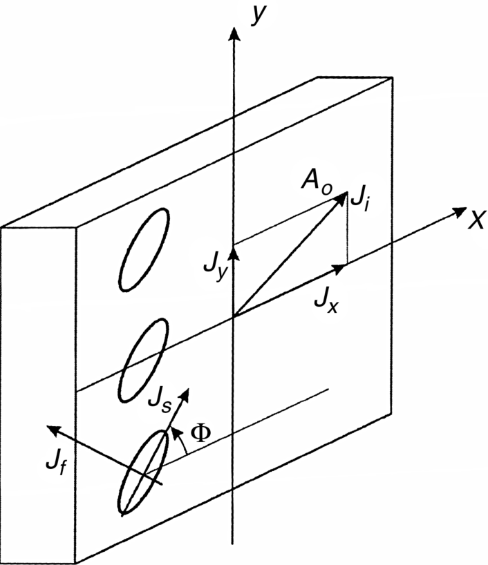
Figure 2.59 A LC retarder plate with the slow and fast Jones vectors Js and Jf.
If the axes of Js and Jf do not coincide with the xy-coordinates of the input, as depicted in Figure 2.60, the coordinates for Ji first have to be rotated by the angle ϕ into JsJf-coordinates. This is performed by the rotation matrix
(2.46)![]()
R(ϕ) as a multiplier on the left of a matrix rotates the coordinates of the matrix for ϕ > 0 in the mathematical positive direction, that is, counterclockwise, while for ϕ < 0 the rotation is clockwise. The new input for the retarder in Figure 2.61 is
(2.47)![]()
and the output of the retarder with T in Equation 2.45b is
(2.48)![]()
Figure 2.60 A LC retarder where the coordinates for Jx and Jy are different from those of Js and Jf.
In [42] the design of a BBR is presented with the constraint for the luminance L as
In the relatively wide range of λ the dependence of the retardation on λ has to be included. It is approximated by
where d is the thickness of the retarder layer, A0 = 0.8646, B0 = 3.7018 · 104 nm2, and C0 = 1.2 · 109 nm4.
In order to meet constraint 2.50 a sequence of retarder films in Figure 2.61 is placed between the polarizer at the input and the analyzer at the output. The films differ in the angles ϕi of the slow axis of the LC molecules with respect to the xy-coordinates of the Jones vector Ji at the input with
(2.51)![]()
Figure 2.61 The sequence of retarders to satisfy requirement(2.49).
The transfer matrix Ti for the retarder film with ϕ = ϕi is
The rotation in Ti has to be performed from the angle ϕi−1 at the output of the film with number i − 1 and with angle ϕi−1 to the xy-coordinates into the angle ϕi of the retarder film number i. The difference ϕi − ϕi−1 is also the phase shift for the retarder i. This leads to the Jones vector J0 at the output given by
The rotator matrix with ϕA and ϕN rotates the output of the last retarder N with the slow axis ϕN into the coordinates of the analyzer at the output given by the angle ϕA to the coordinates. Ji is the input vector in Equation 2.44.
The intensity L of the light at the output and its constraint are given by
where Ju is Re J and Jv is Im J.
With three foils of HW plates with δ = π at 540 nm, the dependency of λ in Equation 2.50, and with crossed polarizers at the input and the output, a BB HW plate with the luminance versus λ in Figure 2.62 was achieved. This represents a substantial improvement over the performance of a single HW plate (HWP). The luminance very closely approximates a constant. The peaks of the films rotated by ϕi occur at different λ-values, thus alleviating the approximation of a constant.
Figure 2.62 The luminous output versus λ of a BB HWP and a single HWP.
The approach with a sequence of retarder films can also be used to compensate the given inhomogeneous luminous output of a stereoscopic projector. If this luminance output is l(λ) the requirement for the correction L is similar to constraint (2.54), namely,
This was applied in [45] with retarders consisting of thin films of polycarbonate (PC) and polymethylmethacrylate (PMMA). The incentive was that, with constraint (2.55), not only a homogeneous luminance but also decreased color shift and diminished crosstalk could be reached. Color shift is created by a change of the retardation dΔn when viewing a display under an oblique angle, because with this angle the refractive index changes according to the index ellipsoid of revolution [3], pp. 124–127 and 34. As compensation for this, the retarders just change the retardation, and this turns out in such a way as to decrease color shift. As the retarders are designed to provide a homogeneous transmittance of light, they also provide a homogeneous black state, which diminishes crosstalk into the desired black state of a display. Equations 2.52 and 2.53 demonstrate that the image the viewer receives in the form of Jp is crucially dependent on the angles ϕi of the retarders or, with the same effect, on the tilting angle of the viewer's head sidewise.
The improvement in the quality of a 3D projection display in terms of homogeneous luminous output, crosstalk, and color shift was investigated in [45]. But first we look at an example of a BBR before any optimization.
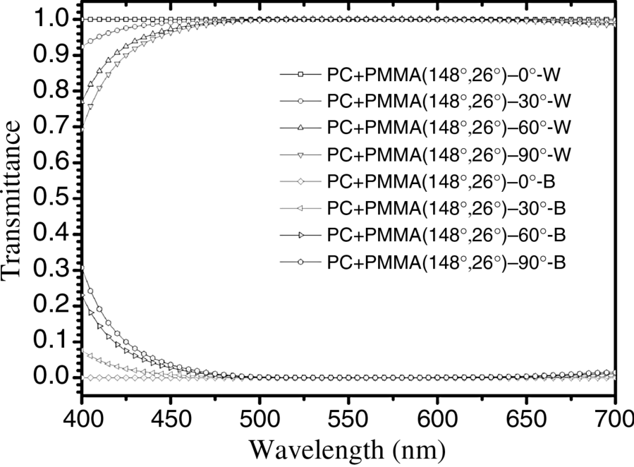
Figure 2.63 depicts the properties of a conventional BBR made out of PC versus wavelength viewed under a head rotation of 0°, the ideal position for which the BBR was designed, and of 30° and 90°. The two ordinates are the phase retardation δ, desired to be π/2, and the difference from the desired output amplitude, being 0 in the ideal case. The deviation from the desired value increases with increasing head rotation angle, especially at lower wavelengths. Figure 2.64 depicts the transmittance in the black state of this conventional BBR versus λ for a head rotation of 30° and 90°. The deviations from black, especially at low wavelengths, indicate that crosstalk is increasing with increasing head rotation. An improvement was achieved by using a sequence of retarder foils according to Equations 2.52 and (2.53). Two retarders were used, one made out of PC the other out of PMMA. Figure 2.65 shows the transmittance of this sequence versus wavelength in the white (W) and the black (B) state at head rotations of 0°, 30°, 60°, and 90°. Viewed under 0° the transmittance in the white and the black of this two-foil compensated retarder is virtually ideal, but it deviates at lower wavelengths with increasing rotation angle. The light leaking into the black state at non-zero head rotation angles indicates crosstalk, but is diminished versus the crosstalk in Figure 2.64, where only one retarder was used. The two-foil approach in Figure 2.65 avoided leakage into the black altogether at a head rotation of 0°.
Figure 2.63 Retardation and amplitude difference versus λ of a conventional BBR viewed under head rotation angles of 30° and 90°.
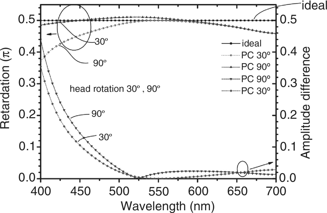
Figure 2.64 Transmittance in the black state of a BBR at head rotation angles of 30° and 90°.
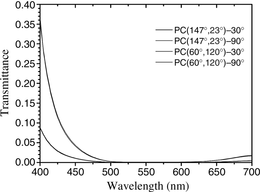
Figure 2.65 Transmittance in the white and black state versus λ of a retarder with two foils made out of PC and PMMA viewed under head rotation angles of 0°, 30°, 60°, and 90°.
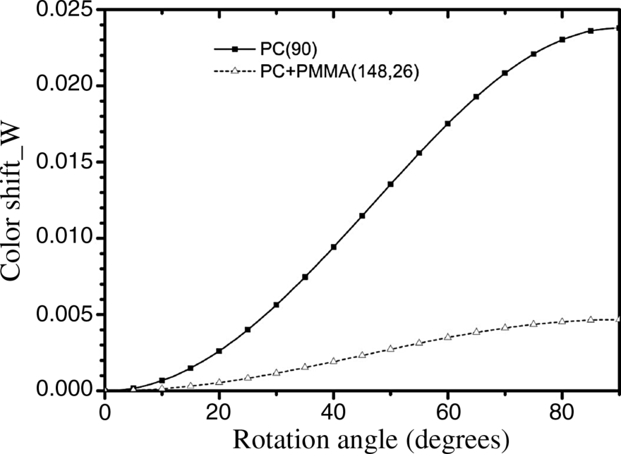
The crosstalk is further exemplified in Figure 2.66 where it is plotted versus the head rotation angle. It is large for only one polarizer, smaller for a one-layer PC retarder, and virtually zero for a two-foil PC + PMMA retarder. The shift of color versus the head rotation angle is depicted in Figure 2.67. The color shift is measured as the distance that the color moves from its desired location in the CIE 1976 chromaticity diagram. This shift in Figure 2.67 is remarkably lower for the two-layer PC + PMMA retarder than for the single layer PC retarder. For a head rotation angle of 0° both of them provide a zero color shift. As mentioned earlier, the degrees of freedom for the design of the sequence of retarder foils are their rotation angles ϕi in Equation 2.52 and the selection of the type of retarder, HWP or QWP (Quarter-Wave Plate). Experiments in [45] revealed that the minimum crosstalk does not occur with the same selection of angles ϕi needed for minimum color shift. The best solutions were found for a sequence of a PC HWP followed by a PMMA QWP. For minimum crosstalk the best angles ϕi for the HWP and the QWP were 148° and 25° respectively, while for minimum color shift they were 58° and 115° for red, 33° and 157° for green, and 133° and 4° for blue respectively. So minimizing both color shift and crosstalk requires a compromise. The results so far were found experimentally.
Figure 2.66 Crosstalk versus head rotation angles for a polarizer, a single foil PC retarder, and a two-foil PC + PMMA retarder.
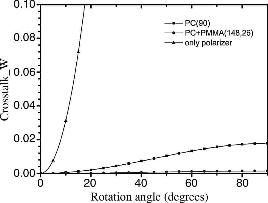
Figure 2.67 Color shift of white versus head rotation angle.
The investigation of sequences of retarders revealed that they can be used both for the optimization of BBRs for the entire range of visible light and for the improvement of existing optical systems with respect to their homogeneity of light output and their diminishing of crosstalk and color shift.
2.6 Interleaved, Simultaneous, and Progressive Addressing of AMOLEDs and AMLCDs
In Section 2.2 a solution of virtually crosstalk-free addressing of LCDs proved that frame frequencies of at least 240 Hz are required. This suppressed motion blur and crosstalk by separating the left and right eye image enough to prevent crosstalk and to minimize blur as outlined in Section 1.4 and in figure 2.5, 2.6 and 2.7a,b. However, the large frame frequency ensues a fast processing by the addressing circuit which for LCDs could be handled in Section 2.2 by using two column lines for the parallel processing of the image data. This is shown by the circuit in Figure 2.25. For OLEDs a virtually crosstalk-free operation was achieved, as treated in Section 2.3.2, by replacing the commonly used progressive addressing and emission of light in Figure 2.3 by simultaneous emission in Figure 2.4. The black insertion between the two images suppressed crosstalk and provided time for the addressing or scanning of the rows.
For AMOLEDs, the introduction of parallel addressing for handling the fast frame rate of 240 Hz, needed to suppress motion blur and crosstalk, was further enhanced in [46] by the same group with the attractive idea of also introducing a parallel input of images by interleaved addressing.
The interleaved addressing and the interleaved emission in Figure 2.68 divide an image into a first image with the pixels E and into a second image with the pixels O. For the following explanations, interleaving according to Figure 2.69 with the weaving geometry H-line weave is used. Each image has half the number of rows and hence half the resolution of the original image. While the O-block is emitting half of the left eye image LO in Figure 2.68, the other half of the left eye image LE is scanned. The scan and emission are performed with 120 Hz, that is, within 8.33 ms. The same applies in the next 120 Hz frame to the halves RO and RE of the right eye image. Hence the time for both halves is 2 · 8.33 ms = 16.66 ms reflecting in the 60 Hz frame in which the images are provided by the image source. Half the number of rows means a doubling of the scan time/row. According to Figure 2.68, the scan time allotted to the interleaved operation is 1/240 s = 4.16 ms resulting for the 1080 rows in a scan time of 4.16/540 = 7.7 μs instead of 3.85 μs for the original image.
Figure 2.68 The operation of interleaved addressing.
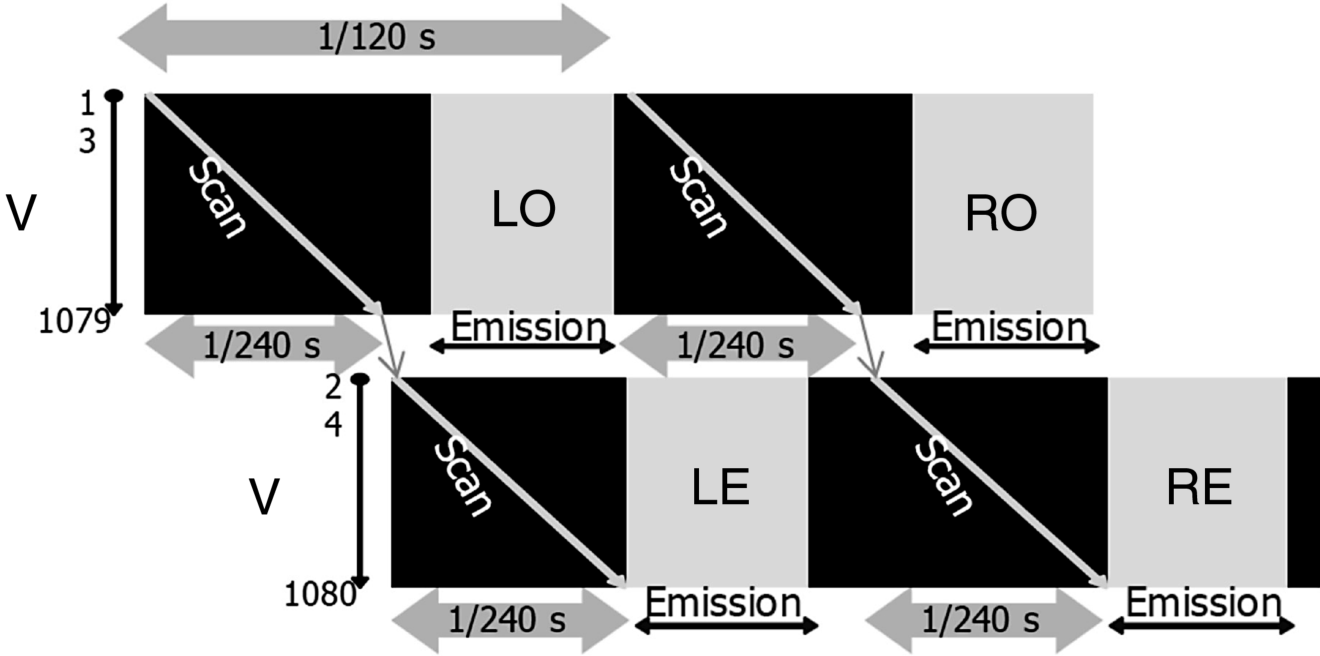
Figure 2.69 Various possibilities to split an image into two halves by different weaving geometries.
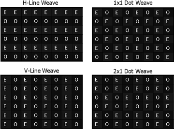
Some more possibilities to split a given image into two different weaves of geometry are depicted in Figure 2.69 and explained in [46].
Of course, there is a penalty to be paid for the benefit of doubling the scan time/row. For each half of the images, the E-block and the O-block, the different addressing circuits in Figure 2.70 are needed. The circuits themselves are equal, but the power lines and the global control inputs GCE and GCO are different. Different power lines avoid changes in the luminance by voltage drops during the emission time of one block, affecting the scan of the other block. This also applies to the degrading capacitive couplings between the blocks.
Figure 2.70 The two different addressing circuits for the interleaved operation.
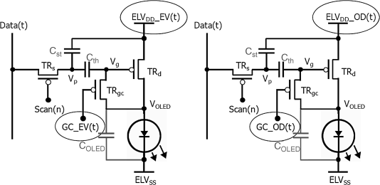
The beginning and the end of the rows in the E-block and the O-block exhibit the jagged edges in Figure 2.71 because of different emission timings. This leads to artifacts which can be reduced by shifting the E and the O emission blocks to be as close together as possible. This was done in Figure 2.72, resulting in a more contiguous emission that reduced the jagged appearance.
Figure 2.71 The jagged view of the edges in interleaved emission.
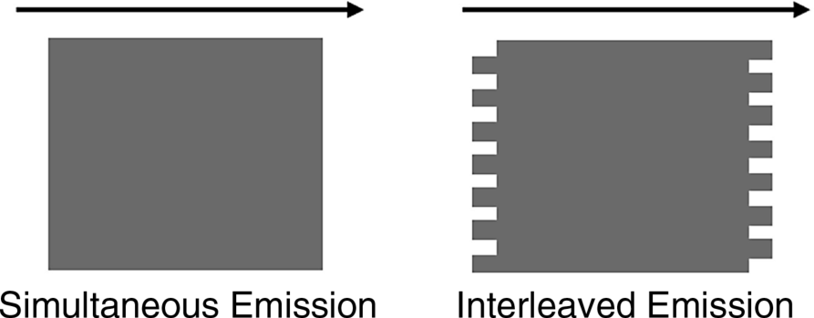
Figure 2.72 The conventional and the contiguous placement of the emitting E- and O-blocks.
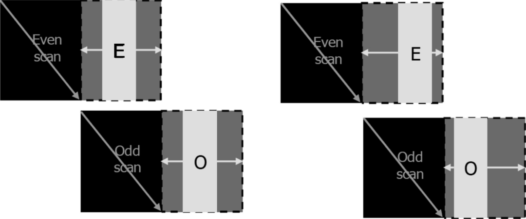
Time-wise, the two pairs of an E-block and an O-block are arranged equally spaced within the 60 Hz frame as shown in Figure 2.73. That way, the images are presented to the eyes of the viewer with a 240 Hz rate which is essential for a virtually blur-free and crosstalk-free 3D perception. In an elegant way this was achieved with the slower 120 Hz processing of the scans.
Figure 2.73 The time-wise equal spacing of the two pairs of the E-block and O-block within the 60 Hz frame.
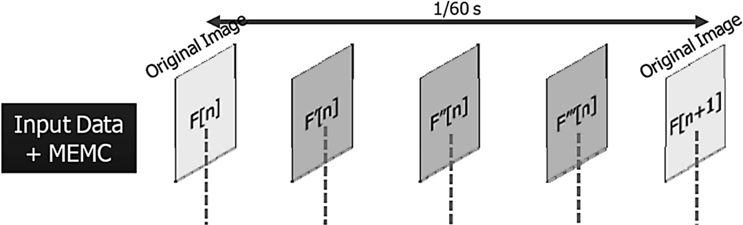
The shutter glasses have to open the right eye view when, for example, the E-image is presented and the left eye view when the O-image is shown.
If the scanning is only performed for the E- and O-pair at the beginning of the 60 Hz frame a 2D image is realized.
Comparing Figure 2.37 for simultaneous emission and Figure 2.68 for interleaved emission, we observe that the latter emission is continuous while the simultaneous emission possesses two spikes lasting only half the 60 Hz frame time. For the same luminance only half the peak power is required in the interleaved version compared to the simultaneous version. The interweaved version offering a double scan time exhibits the consequences of either using half the number of driver ICs per image or increasing the resolution of the 3D image.
In [47] two more modifications of the progressive and the simultaneous emission of OLEDs are proposed.
The first proposal in Figure 2.74 uses the progressive scan and both the progressive and the simultaneous emission in the same operation. To achieve this, the emission control EM(n) in the addressing circuit in Figure 2.75a is required. As visualized in Figures 2.74 and 2.75b, progressive addressing is applied for the progressive emission of the left eye image L, for which the control EM(n) in Figure 2.75a is conducting. During the progressive scan for the image R in Figures 2.74 and 2.75b the control EM(n) in Figure 2.75a is blocked and is again rendered conductive after the particular row for R has been scanned. That way, a simultaneous emission is achieved. This works perfectly for AMOLEDs. For AMLCDs (Active Matrix Liquid Crystal Displays) the luminance of the images is inhomogeneous because in the first row the LC molecules have the longest time to rotate into their desired position, while this time is shortest for the last row. This is not visible for AMOLEDs because their pixels assume their desired luminance in a virtually zero response time. The block scan time in Figure 2.68 is reduced from 1/2 for the progressive scan and emission to 1/3 of the frame time, corresponding to 180 Hz.
Figure 2.74 The progressive 180 Hz scan and the progressive and simultaneous emission in a 60 Hz frame.
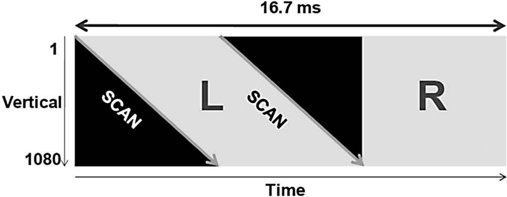
Figure 2.75 The progressive and simultaneous emission with (a) the addressing circuit and (b) the timing for the progressive scan.
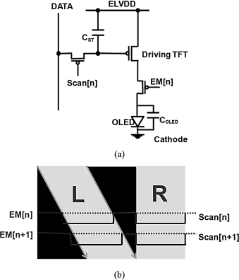
The second proposed method is most effective and reduces the block scan time to zero. To achieve this, the addressing circuits in Figure 2.76a for AMLCDs and in Figure 2.76b for AMOLEDs have to be used.
Figure 2.76 The addressing circuits (a) for an AMLCD and (b) for an AMOLED for a zero black scan time and 120 Hz driving.
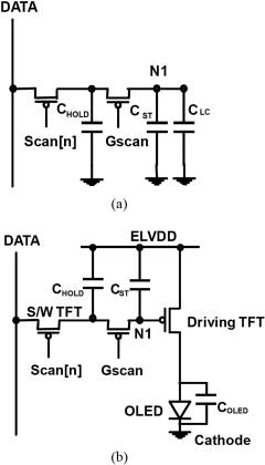
The image data is progressively stored in the capacitor CHold in Figure 2.76a and 2.76b while the TFT with gate input G scan is blocked. This storage happens while the previous images stored on the capacitors Cst are emitted by the LCD and the OLEDs as shown for the left eye image L in Figure 2.77. In the next step the charge Vdata CHold is redistributed onto the capacitors CHold, Cst and in the case of the LCD also onto CLC by rendering the TFT with the gate G scan conductive. That way, the image R in Figure 2.77 with the data Vdata which was stored on CHold is simultaneously emitted, in the case of the OLEDs virtually immediately, and in the case of the slower LCDs gradually with a noticeable response time.
Figure 2.77 The emission for the left (L) and right (R) image for 120 Hz driving.
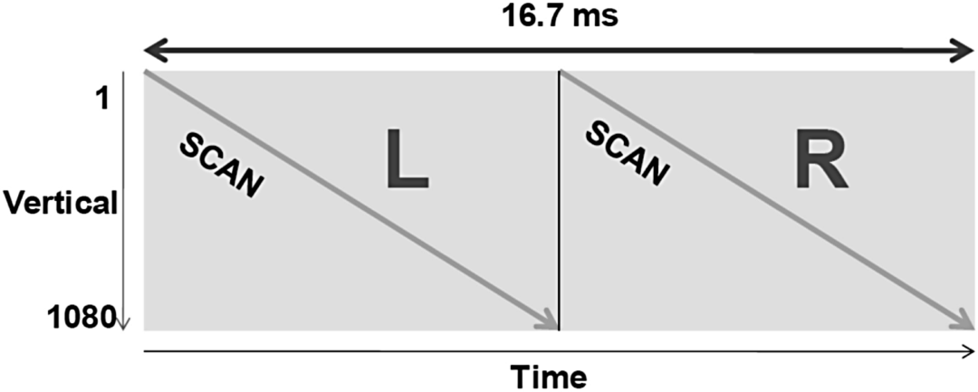
With the charge ![]() Cst of the previous image, the redistribution of the charge provides the OLED data voltage VN1 as
Cst of the previous image, the redistribution of the charge provides the OLED data voltage VN1 as
(2.56)![]()
This equation holds only for AMOLEDs because, for AMLCDs, the capacitor CLC also participates in the distribution of the charge.
This second addressing scheme is most effective and provides simultaneous emissions for the left (L) and the right (R) eye in Figure 2.77, while the black insertion was reduced to zero, thus maximizing the luminance. The resulting emission frequency in Figure 2.77 is 120 Hz, which is also the scan frequency with, again, a further enhanced scan time.
With the picture frequency of 120 Hz the reduction of blur associated with 240 Hz seems to be partly sacrificed in favor of the advantages of power consumption and ease of addressing that will be presented below. The causes for blur are both the holding of the image during the frame time and the optical response time of the device. For the fast OLEDs only the holding time still plays a role, while for the LCDs both causes are present.
The addressing scheme in Figure 2.77 may present some more difficulties for LCDs due to their slow rotation of the LC molecules into their desired position. This limits uniformity of luminance and may increase crosstalk.
Another problem is that, for the same reason, the LC shutter glasses also do not react abruptly but require a response time for switching into the on and off state. As a remedy for the shutter problem, a black insertion (BI) between the various emission states is proposed in [48] as shown for various addressing schemes in Figure. A duration of the BI of 2.5 ms was found to be sufficient.
Figure 2.78 A black insertion (BI) (a) for a 240 Hz progressive scan and emission, (b) for a 240 Hz simultaneous emission, (c) for a progressive 180 Hz scan and emission and a simultaneous emission, and (d) a 120 Hz simultaneous emission.
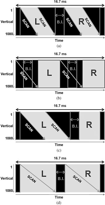
In the following figures, operations with a zero BI and a 2.5 ms BI shutter response time are compared.
The first topic in Figure 2.79 is the percentage of the luminance in AMLCDs for various emissions realized in Figure 2.78, where 100% stands for the progressive emission at 240 Hz. The simultaneous emission exhibits the same luminance for zero BI and for non-zero BI. The emissions for the first and second new proposals are larger because the time for emission at 180 Hz and 120 Hz is larger. For the non-zero BI cases the luminances are of course always lower.
Figure 2.79 The luminance in LCDs for four types of emission.
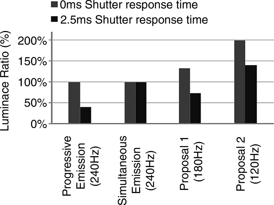
Figure 2.80 shows the available scan time for the same four types of emissions. The available scan time increases with decreasing frame frequencies. A larger scan time minimizes the influence of the RC delay and hence improves image quality.
Figure 2.80 The available scan time for LCDs for four types of emission.
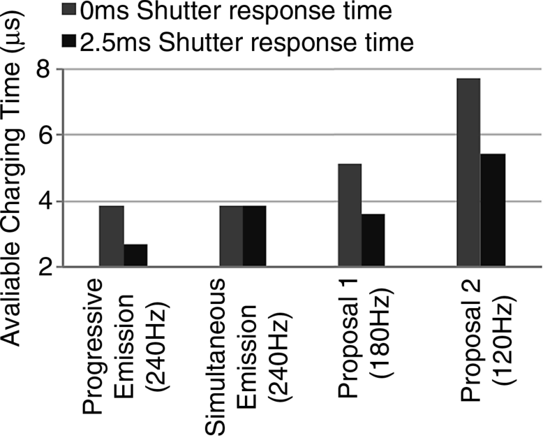
For AMOLEDs the maximum current for the same luminance compared to 100% for zero BI at progressive emission is depicted in Figure 2.81. A non-zero BI always requires more current. The necessary current for the case of a zero BI decreases with decreasing driving frequency because the image is presented longer. For simultaneous emission at 240 Hz, there is remarkably no difference between a zero and a non-zero BI.
Figure 2.81 The maximum current through AMOLEDs for four types of emission.
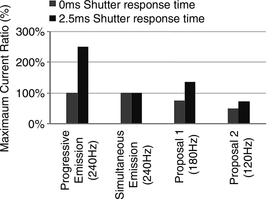
The addressing schemes discussed fit very well to AMOLEDs because their optical response time is very short. However, they still cannot be manufactured as efficiently as LCDs. On the other hand, as already mentioned, LCDs possess a slower increase of luminance, which is especially noticeable as a low illumination at frame rates larger than 60 Hz. The slow decay of luminance can cause crosstalk. A remedy could be the enhancement of switching speed as presented in [3], p. 334. The essence of that approach, briefly outlined, is to provide a larger driving voltage resulting in an increased torque for the rotation of the LC molecules. The boost in torque was introduced during the available scan time in [48, 49]. As this time is, as a rule, very short, the boost of torque is not strong enough. Therefore the enhanced voltage is held beyond the scan time until an additional TFT in each pixel reduces it to the desired voltage. The selection of the boost voltage and of the duration of the boost allow the response time to be decreased to about 0.1 ms. This leads the LCD closer to the time-wise operation of an OLED, which might be used for faster and virtually blur- and crosstalk-free 3D perception in LCDs.
The operation of a 3D display in the 2D mode, which will still be required for a long time, is depicted in Figure 2.82 [50]. The progressive scan and emission (PE) in Figure 2.82 is the conventional mode for a 2D display. Operation with the simultaneous emission (SE) applying a conventional 60 Hz progressive scan is shown in Figure 2.83a. If this progressive scan is increased to 240 Hz, the left (L) and the right (R) images needed for the 3D mode are implemented as shown in Figure 2.83b.
Figure 2.82 The 60 Hz progressive scan and emission (PE) for a 2D display.
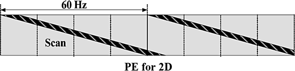
Figure 2.83 The simultaneous emission (SE) (a) for a 60 Hz 2D display and (b) for a 240 Hz 3D display.
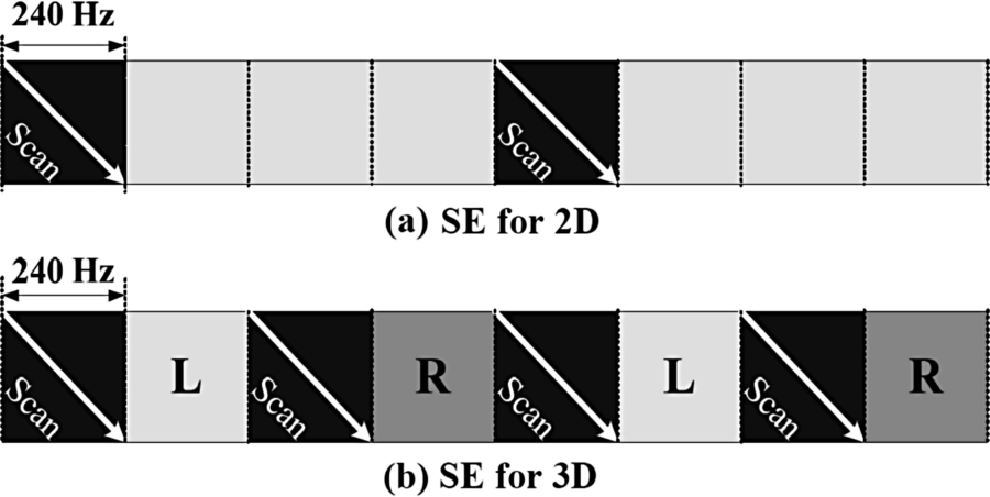
In addition, an improved driving circuit is presented which suppresses the unnecessary OLED current during the initialization period and which provides a threshold compensation [50].
In the future, oxide TFTs [51] could play a role in fast driving. They possess InGaZO, an oxide, as the semiconductor. The cross-section of an InGaZO TFT is shown in Figure 2.84 together with the layers needed for addressing an OLED [52]. Mobilities achieved are less than or equal to 35 cm2/V s which is considerably higher than for a-Si TFTs. With nano-dot doping of the semiconductor by polystyrene spheres the mobility could be increased to 79 cm2/V s [53] while still keeping the gate–source voltages in the 10 V range.
Figure 2.84 Cross-section of an IGZO TFT with the layers needed for addressing an OLED.
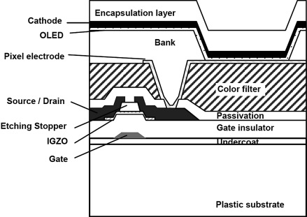
2.7 Photo-Induced Alignment for Retarders and Beam Splitters
Retarders and also beam splitters have become essential components for the implementation of stereoscopic displays. In this book their physical operation and their application for 3D displays have been outlined. In view of their importance it is also indispensable to know how they can be made so as to achieve high transmittance as well as polarization uniformity and the stability required for 3D perception. To achieve these properties the alignment of the directors of LC molecules has to be uniaxial with a defined tilt angle and stable over time and temperature. A technology to achieve this is photo alignment, a non-mechanical approach based on anisotropic photo polymerization [54]. For more information, readers are referred to [55, 56].
The author gratefully acknowledges permission to reproduce figures granted by the institution named below. The sources of the figures are also listed below together with their corresponding numbers in this book.
Society for Information Display (SID)
Journal of the SID (J. SID)
J. SID, 17.5, p. 407, figures 2.1–2.3, 2.6
Reproduced as Figures 2.53–2.55, 2.57
| SID – Symposia and Conferences | |
| SID 08 p. 448, figure 1 | reproduced as Figure 2.4 |
| p. 450, figure 6 | reproduced as Figure 2.5 |
| p. 261, figures 4, 5, 7 | reproduced as Figures 2.6–2.8 |
| p. 444, figures 1a, 1b | reproduced as Figures 2.9 2.10 |
| SID 07 p. 1165, figures 2a, 3 | reproduced as Figures 2.13, 2.14 |
| SID 10 p. 5, figure 2 | reproduced as Figure 2.15 |
| p. 7 figures, figures 8, 9 | reproduced as Figures 2.17 2.18 |
| SID 08 p. 458, figure 4 | reproduced as Figure 2.19 |
| SID 09 p. 425, figure 2 | reproduced as Figure 2.20 |
| SID 09 p. 424, figure 1 | reproduced as Figure 2.21 |
| p. 427, figure 8 | reproduced as Figure 2.22 |
| p. 425, figures 3,4, 5, 7 | reproduced as Figures 2.24–2.27 |
| p. 349, figures 1, 3b, 4a, 4b | reproduced as Figures 2.29–2.31a,b |
| p. 428, figures 1, 2, 6 | reproduced as Figures 2.32–2.34 |
| SID 10 p. 763, figures 2, 3, 6, 7, 8 | reproduced as Figures 2.35–2.39 |
| p. 759, figures 2a,b, 3, 4 | reproduced as Figures 2.40, 2.42, 2.41 |
| SID 07 p. 1159, figures 1, 2, 3 | reproduced as Figures 2.43–2.45 |
| SID 10 p. 872, figures 1, 2, 3, 4 | reproduced as Figures 2.46, 2.49, 2.48, 2.50 |
| p. 127, figures 3, 7 | reproduced as Figures 2.51, 2.52a,b |
| p. 868, figure 4 | reproduced as Figure 2.56 |
| p. 13, figures 1, 2 | reproduced as Figures 2.58a,b |
| p. 9, figure 1 | reproduced as Figure 2.59 |
| p. 10, figure 3 | reproduced as Figure 2.61 |
| SID 07 p. 1390, figure 1, 2 | reproduced as Figures 2.60 2.62 |
| SID 10 p. 17, figures 2.3a,b, 4, 5, 6 | reproduced as Figures 2.63–2.65, 2.60, 2.67 |
| SID 11 p. 264, figures 2, 3, 4, 5, 6, 8 | reproduced as Figures 2.68–2.73 |
| p. 273, figures 3, 4, 5, 6, 7, 8, 9, 10 | reproduced as Figures 2.74 , 2.75a,b, 2.76a,b, 2.77 ,2.78a–d, 2.79–2.81 |
| p. 268, figures 1a–c | reproduced as Figures 2.82, 2.83a,b |
| p. 21, figure 1 | reproduced as Figure 2.84 |
1. Tsai, C.H. et al. (2008) The pursuit of high definition 3D display technology. SID 08, p. 456.
2. Born, M. and Wolf, E. (1980) Principle of Optics, Pergamon Press, Oxford.
3. Lueder, E. (2010) Liquid Crystal Displays – Addressing Schemes and Electro-Optical Effects, 2nd edn, John Wiley & Sons, Ltd, Chichester, pp. 21–23.
4. Lee, C.T. et al. (2008) The improvement of in-cell microretarder for stereoscopic LCD fabrication. SID 08, p. 448.
5. Wu, Y.J. et al. (2008) Stereoscopic 3D displays using patterned retarders. SID 08, p. 260.
6. Kang, H. et al. (2010) A novel polarizer glasses-type 3D display with a patterned retarder. SID 10, p. 1.
7. Oh, J.H. (2008) Stereoscopic TFT-LCD with wire grid polarizer and retarder. SID 08, p. 444.
8. Oh, J.H. et al. (2007) High resolution stereoscopic TFT-LCD with wire grid polarizer. SID 07, p. 1184.
9. Lin, H.T. et al. (2010) A new approach to dynamic polarization 3D LCD. SID 10, p. 5.
10. Kim, S.S. et al. (2009) World's first 240Hz TFT-LCD technology for Full-HD LCD-TV and its application to 3D display. SID 09, p. 424.
11. Park, S.B. et al. (2010) A novel charge shared SPVA technology. SID 07, p. 1252.
12. Kim, S.S. et al. (2004) New technologies for advanced LCD-TV performance. J. SID, 12, 353.
13. Kim, T. et al. (2005) Black frame insertion technique with charge share. Eurodisplay, P 2, 152.
14. Lueder, E. (2010) Liquid Crystal Displays – Addressing Schemes and Electro-Optical Effects, 2nd edn, John Wiley & Sons, Ltd, Chichester, pp. 293–295.
15. Shestak, S. and Kim, D. (2003) Application of π-cells in time-multiplexed stereoscopic and autostereoscopic displays based on LCD panels. SPIE Proc., 5006, 136.
16. Jung, S.M. et al. (2009) A novel polarizer glasses-type 3D display with an active retarder. SID 09, p. 348.
17. Kumagawa, K. et al. (2002) Fast response OCB-LCD for TV applications. SID 02, p. 1288.
18. Nakao, K. et al. (2007) OCB-LCD with new driving method having fast response of 2-3ms MPRT and high contrast ratio of 1000:1. SID 07, p. 138.
19. Suzuki, D. et al. (2009) Cross talk free 3D display with time sequential OCB-LCD. SID 09, p. 428.
20. Pastoor, S., (1995) Human factors of 3D imaging. Results of recent research at Heinrich-Hertz-Institut-Berlin. IDW Proceedings 95, p. 69.
21. Kim, D.S. et al. (2010) New 240Hz driving method for full HD and high quality 3D LCD TV. SID 10, p. 762.
22. Lee, B.W. et al. (2010) Novel simultaneous emission driving scheme for cross talk free 3D AMOLED TV. SID 10, p. 758.
23. Yano, S. et al. (2002) A study of visual fatigue and visual discomfort for 3D HDTV/HDTV images. Displays, 23, 191.
24. Farné, M. (1977) Brightness as an indicator to distance: relative brightness per se or contrast with the background. Perception, 6, 287.
25. Takahashi, S. et al. (2010) Control of subjective depth on 3D displays by a quantified monocular depth cue. SID 10, p. 870.
26. Chang, Y.C. et al. (2010) Cross talk suppression by image processing in 3D display. SID 10, p. 124.
27. Jorke, H. et al. (2009) Advanced stereo projection using interference filters. J. SID, 17.5, 407.
28. Simon, A. et al. (2010) Recent progress in interference-filter based stereoscopic 3D LCD. SID 10, p. 867.
29. Jorke, H. and Fritz, M. (2006) Stereo projection using interference filters. Proceedings of SPIE-IS and T, Electronic Imaging 6055, 60505G.
30. Kelly, D.H. (1953) Optical projection of beam controlled object fields, US Patent 2 958 258, 1960, filed.
31. Li, L. et al. (1998) High efficiency projection display with novel thin film polarizing beam splitters. SID 98, p. 686.
32. Robinson, M. et al. (2003) Wide field of view compensation scheme for cube polarizing beam splitters. SID 03, p. 874.
33. Rosenbluth, A.E. et al. (1998) Contrast properties of reflective liquid crystal light valves in projection displays. IBM J. Res. Dev., 42 (3–4), 359.
34. Cline, R. et al. (2002) Thermal stress birefringence in LCOS projection displays. Displays, 23.3, 151.
35. Bothroyd, S.K. (2010) Simultaneous projection of stereoscopic 3D left- and right-eye images in orthogonal polarization through a single lens. SID 10, p. 13.
36. Sekmé, A. (1998) Projection lens system, US Patent 5822129, Oct. 13.
37. Hoepfner, C. (2006) Phlatlight photonic lattice LEDs for RPVT light engines. SID 06, p. 1808.
38. Bogaert, L. et al. (2008) Projection display for the generation of two orthogonal polarized images using liquid crystal on silicon panels and light emitting diodes. Appl. Opt., 47, 1535.
39. Bogaert, L. et al. (2009) Design of a compact projection display for the visualization of 3D images using polarization sensitive eye glasses. J. SID, 17.7, 603.
40. Bogaert, L. et al. (2010) Efficient polarization based stereoscopic projector with extended color gamut: combining two projectors into one. SID 10, p. 9.
41. Murat, M. et al. (2009) Two LCOS full color projector with efficient LED illumination engine. Displays, 30, 155.
42. Kwok, H.S. et al. (2007) Extremely broadband retardation films. SID 07, p. 1390.
43. Jones, R.C. (1941) New calculus for the treatment of optical systems. J. Opt. Soc. Am., 31, 488.
44. Yeh, P. and Gu, C. (1999)Optics of Liquid Crystal Displays, John Wiley & Sons, Inc, New York.
45. Chang, Y.H. et al. (2010) Novel broad band retarder evaluation metrics for 3D projection displays. SID 10, p. 17.
46. Lee, B.W. et al. (2011) 120Hz 3D driving for AMOLED with interleaved scan and emission operation. SID 11, p. 264.
47. Hwang, Y.I. et al. (2010) Low frequency driving methods for 3D displays. SID 11, p. 272.
48. Song, J.K. et al. (2004) OCCII: novel method for fast response time in PVA mode. SID 04, p. 1344.
49. Lueder, E., (2004) Shortcomings and remedies of AM addressing for LCDs and OLEDs. Workshop SID Asia Display/IMID 04, p. 65.
50. Cheng, S.W. et al. (2011) Driving method for a 2D-3D switchable AMOLED display using progressive or simultaneous emission. SID 11, p. 268.
51. Nomura, K. et al. (2004) Room temperature fabrication of transparent flexible thin-film transistors using amorphous oxide semiconductors. Nature, 432, 488.
52. Miura, K. et al. (2011) Low temperature processed IG ZO TFT for flexible AMOLED with integrated gate driver circuits. SID 11, p. 21.
53. Zan, H.W. et al. (2011) High performance IG ZO TFT with nano-dots doping. SID 11, p. 28.
54. Schadt, M. et al. (1995) Photo-induced alignment and patterning of hybrid liquid crystalline polymer films on single substrates. Jpn. J. Appl. Phys., 34, L764.
55. Schadt, M. (1997) Liquid crystal material and liquid crystal displays. Annu. Rev. Mater. Sci., 27(3), p. 305.
56. Schadt, M. (2011) Photo-alignment and alignment patterning of liquid crystals. SID Seminar Lecture Notes, M–9/1.
57. Sechrist, S. (2011) Display Week 2011 Review: 3D, Inf. Display 7/8, p. 16.