
Static Circuits
This chapter explores the design of systems with static CMOS logic and memory elements: flip-flops, transparent latches, and pulsed latches. Most students are taught that the purpose of memory elements is to retain state. The chapter begins by arguing that memory elements can be understood more easily if viewed as a way of enforcing sequencing. It then defines some terminology regarding confusing meanings of the words “static” and “dynamic.” The emphasis of the chapter is on comparing the operation of flip-flops, transparent latches, and pulsed latches. We look at how sequencing overhead, time borrowing, and hold time requirements affect each type of memory element. We then survey the literature about circuit implementations of the memory elements. The chapter concludes with a historical perspective of memory elements used in commercial processors and recommendations of what you should use for your systems.
Clocking and memory elements are highly interdependent. In general, we will assume that a single clock is distributed globally across the system and that it may be locally complemented or otherwise modified as necessary. We will look at clock generation and distribution more closely in Chapter 5.
2.1 Preliminaries
Before examining specific static circuits, let’s begin with a more philosophical discussion of the purpose of memory elements and the often contradictory terminology of static and dynamic elements.
2.1.1 Purpose of Memory Elements
A static CMOS logic system consists of blocks of static CMOS combinational logic interspersed with memory elements. The purpose of the memory elements is not so much to remember anything as to enforce sequencing, distinguishing this from previous and from next. If memory elements were not used, fast signals might race ahead and catch up with slow signals from a different operation, resulting in hopeless confusion. Thus, an ideal memory element should slow down the early signals while adding no delay to the signals that are already late. Real memory elements generally delay even late elements; this wasted time is the sequencing overhead. We would like to build systems with the smallest possible sequencing overhead.
This idea of using memory elements for sequencing at first might seem to conflict with the idea that memory elements hold state, as undergraduates learn when studying finite state machines (FSMs). This conflict is illusory. Any static CMOS circuit can hold state: if the inputs do not change, the output will not change. The real issue is controlling when a system advances from one state to another. From this point of view, it is clear that the role of memory elements in FSMs is also to enforce sequence of state changes.
Another advantage of looking at memory elements as enforcing sequencing rather than storing state is that we can more clearly understand more unconventional circuit structures. Flip-flop systems can be equally well understood from the state storage or sequencing perspectives, partially explaining why they are so easy for designers to grasp. However, transparent latch and pulsed latch systems use two and one latch per cycle, respectively. If you attempt to point to a place in the circuit where state is stored, it is easy to become confused. Later in this chapter, we will show how both methods are adequate to enforce sequencing, which is all that really matters. Similarly, designers who believe latches are necessary to store state will be very confused by skew-tolerant domino circuits that eliminate the latches. On the other hand, it is easier to see that skew-tolerant domino circuits properly enforce sequencing and thus operate correctly.
Finally, this view of sequencing dispels some myths about asynchronous systems. Some asynchronous proponents argue that asynchronous design is good because it eliminates clocking overhead by avoiding the distribution of high-speed clocks [66]. However, when we view memory elements as sequencing devices, we see that all systems, synchronous or asynchronous, must pay some sequencing overhead because it is impossible to slow the early signals without slightly delaying the late signals. Asynchronous designs merely replace the problem of distributing high-speed clocks with the problem of distributing high-speed sequencing control signals.
2.1.2 Terminology
We will frequently use the terms “static” and “dynamic,” which unfortunately have two orthogonal meanings. Most of the time we use the terms to describe the type of circuit family. Static circuits refer to circuits in which the logic gates are unclocked: static cmos, pseudo-nmos, pass-transistor logic, and so on. Dynamic circuits refer to circuits with clocked logic gates: especially domino, but also Zipper logic and precharged RAMs and programmable logic arrays (PLAs). A second meaning of the words is whether a memory element will retain its value indefinitely. Static storage employs some sort of feedback to retain the output indefinitely even if the clock is stopped. Dynamic storage stores the output voltage as charge on a capacitor, which may leak away if not periodically refreshed.
To make matters more confusing, a particular circuit may independently be described as using static or dynamic logic and static or dynamic storage. For example, most systems are built from static logic with static storage. However, the Alpha 21164 uses blocks of static logic with dynamic storage [26], meaning that the processor has a minimum operating frequency so that it does not lose data stored in the latches. The Alpha 21164 also uses blocks of domino (i.e., dynamic logic) with dynamic storage. Most other processors use domino with static storage so that if they were placed in a notebook computer and the clock was stopped during sleep mode, the processor could wake up and pick up from where it left off without having lost information.
In this book, the terms “static” and “dynamic” will generally be used in the first context of circuit families. This chapter describes the sequencing of static circuits. The next chapter describes the sequencing of domino (dynamic) circuits. In each chapter, we will explore the transistor implementations of storage elements, in which the second context of the words is important. Generally we will present the dynamic form of each element first, then discuss how feedback can be introduced to staticize the element.
2.2 Static Memory Elements
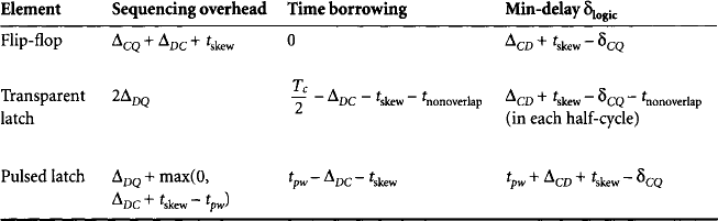
Although there are a multitude of possible memory elements, including S-R latches and J-K flip-flops, most cmos systems are built with just three types of memory elements: edge-triggered flip-flops, transparent latches, and pulsed latches. Transparent and pulsed latch systems are sometimes called two- and one-phase latch systems, respectively. There is some confusion about terminology in the industry, which this section seeks to clear up; in particular, pulsed latches are commonly and confusingly referred to as “edge-triggered flip-flops.” All three elements have clock and data inputs and an output. Depending on the design, the output may use true, complementary, or both polarities.
The section begins with timing diagrams illustrating the three memory elements. It then analyzes the sequencing overhead of each element. Latches are particularly interesting because they allow time borrowing, which is described in more detail. Finally, the min-delay issues involving hold time are described.
2.2.1 Timing Diagrams
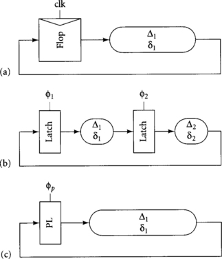
Edge-triggered flip-flops are also known as master-slave or D flip-flops. Their timing is shown in Figure 2.1. When the clock rises, the data input is sampled and transferred to the output after a delay of ΔCQ. At all other times, the data input and output are unrelated. For the correct value to be sampled, data inputs must stabilize a setup time ΔDC before the rising edge of the clock and must remain stable for a hold time ΔCD after the rising edge.
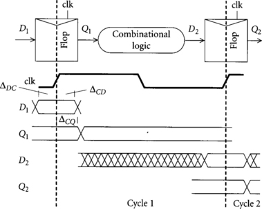
We can check that memory elements properly sequence data by making sure that data from this cycle does not mix with data from the previous or next cycles. This is clear for a flip-flop because all data advances on the rising edge of the clock and at no other time.
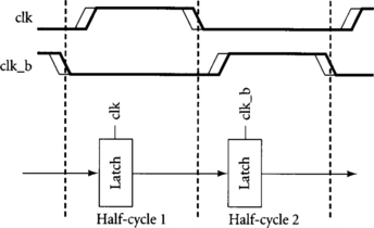
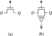
Transparent latches are also known as half-latches, D-latches, or two-phase latches. Their timing is shown in Figure 2.2. When the clock is high, the output tracks the input with a lag of ΔDQ. When the clock is low, the output holds its last value and ceases to track the input. For the correct value to be sampled, the data must stabilize a setup time ΔDC before the falling edge of the clock and must remain stable for a hold time ΔCD after the falling edge. It is confusing to call a latch on or off because it is not clear whether on means that the latch is passing data or on means that the latch is latching (i.e., holding old data). Instead, we will use the terms “transparent” and “opaque.” To build a sequential system, two half-latches must be used in each cycle. One is transparent for the first part of the cycle, while the other is transparent for the second part of the cycle using a locally complemented version of the clock, clk_b.
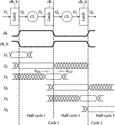
Latches may be placed at any point in the half-cycle; the only constraint is that there must be one latch in each half-cycle. Many designers think of latches at the end of the half-cycle. In Section 1.3, we illustrated latches in the middle of the half-cycle. We will discuss the relative advantages of these choices in Section 4.1. In any event, sequencing is enforced because there is always an opaque latch between data in one cycle and data in another cycle.
Pulsed latches, also known as one-phase or glitch latches, behave exactly as transparent latches, but are given a short pulse of width tpw produced by some local clock generator instead of the usual 50% duty cycle clock. Therefore, only one pulsed latch is necessary in each cycle. Their timing is shown in Figure 2.3. Data must set up and hold around the falling edge of the pulse, just as it does around the falling edge of a transparent latch clock.
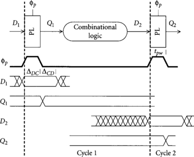
Pulsed latches enforce sequencing in much the same way as flip-flops. If the pulse is narrow enough, it begins to resemble an edge trigger. For this reason, pulsed latches are sometimes misleadingly referred to as “edge-triggered flip-flops.” We will be careful to avoid this because the sequencing overhead differs in important ways. As long as the pulse is shorter than the time for data to propagate through the logic between pulsed latches, the pulse will end before new data arrives and data will be safely sequenced.
2.2.2 Sequencing Overhead
Ideally, the cycle time of a system should equal the propagation delay through the longest logic path. Unfortunately, real sequential systems introduce overhead that increases the cycle time from three sources: propagation delay, setup time, and clock skew. In this section, we will look at the sequencing overhead of each type of memory element, obtaining equations in the form
In Section 1.1 we found that flip-flops pay all three sources of overhead. Data is launched on the rising edge of one flip-flop. It must propagate to the Q output, then pass through the logic, and then arrive at the next flip-flop a setup time before the clock rises again. Any skew between the clocks that could cause the first flip-flop to fire late or the second flip-flop to sample early must be budgeted in the cycle time Tc:
In Section 1.3 we saw that transparent latches can be used such that data arrives more than a setup time before the falling edge of the clock, even in the event of clock skew. The data will promptly propagate through the latch and subsequent logic may begin. Therefore, neither setup time nor clock skew must be budgeted in the cycle time. However, there are two latches in each cycle, so two latch propagation delays must be included:
There is widespread misunderstanding about the overhead in transparent latch systems. Many designers and even textbooks [92] mistakenly budget setup time or clock skew in the cycle time. Worse yet, some realize their error but continue to budget setup time on the grounds that they are “being conservative.” In actuality, they are just forcing overdesign of the sections of the chip that use transparent latches. This overdesign leads to more area, higher power, and longer time to market. They may argue that the chip will run faster if the margin was unnecessary, but if the chip contains any critical paths involving domino or flip-flops, those paths will limit cycle time and the margin in the transparent latch blocks will go unused. It is much better to add margin only for overhead that actually exists.
Also, notice that our analysis of latches did not depend on the duty cycles of the clocks. For example, the latches could be controlled by nonoverlapping clocks without increasing the cycle time. Nonoverlapping clocks will be discussed further in Section 2.2.4 and in Chapter 6.
Pulsed latches are the most interesting to analyze because their overhead depends on the width of the pulse. Data must set up before the falling edge of the pulse, even in the event of clock skew. This time required may be before or after the actual rising edge of the pulse, depending on pulse width and clock skew, as illustrated in Figure 2.4. If the pulse is wider than the setup time plus clock skew, the data can arrive while the pulsed latch is transparent and pass through with only a single latch propagation delay. When the pulse is narrow, data must arrive by a setup time and clock skew before the nominal falling edge. This required time can be earlier than the actual rising edge of the pulse. Therefore, the data may sit idle for some time until the latch becomes transparent, increasing the overhead in the case of short pulse widths. Later, we will see that long pulse widths cause hold time difficulties, so pulsed latches face an inherent trade-off:
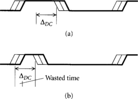
Figure 2.4 Effect of pulse width on sequencing overhead: pulse width greater than setup time (a) and pulse width less than setup time (b)
In summary, flip-flops always have the greatest sequencing overhead and are thus costly for systems with short cycle times in which sequencing overhead matters. Nevertheless, they remain popular for lower-performance systems because they are well understood by designers, require only a single clock wire, and are supported by even the least-sophisticated timing analyzers. Transparent latches require two latch propagation delays, but hide clock skew from the cycle time. Pulsed latches are potentially the fastest because with a sufficiently wide pulse they can hide clock skew and only introduce a single latch propagation delay. This speed comes at the expense of strict min-delay constraints.
2.2.3 Time Borrowing
We have seen that a principal advantage of transparent latches over flip-flops is the softer edges that allow data to propagate through the latch as soon as it arrives instead of waiting for a clock edge. Therefore, logic does not have to be divided exactly into half-cycles. Some logic blocks can be longer while others are shorter, and the latch-based system will tend to operate at the average of the delays; a flip-flop-based system would operate at the longest delay. This ability of slow logic in one half-cycle to use time nominally allocated to faster logic in another half-cycle is called time borrowing or cycle stealing.
The exact use of time borrowing depends on the placement of latches. If latches are nominally placed at the beginning of half-cycles, as was done in Figure 2.2, we say that when data arrives late from one half-cycle, it can borrow time forward into the next half-cycle. If latches are nominally placed at the end of half-cycles, we say that if the data arrives early at the latch, the next half-cycle can borrow time backward by starting as soon as the data arrived instead of waiting for the early half-cycle to end. In systems constructed entirely of transparent latches, it does not matter whether we think of time borrowing as forward or backward. In systems interfacing transparent latches to flip-flops or domino gates that introduce hard edges, the direction of time borrowing becomes more important, as we shall see in Section 4.1.1.
Moreover, time borrowing may operate over multiple half-cycles. In the case of forward borrowing, data may arrive late at a latch. If the logic after the latch requires exactly half of a cycle, the result will arrive late at the following latch. This borrowing may continue indefinitely so long as the data never arrives so late at a latch that the setup time is violated.
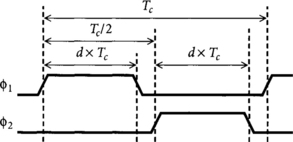
Let us examine how much time borrowing is possible in any half-cycle for transparent latches. For the purpose of illustration, assume that data departs a latch in half-cycle 1 at the rising edge of the clock, as shown in Figure 2.5. The data nominally arrives at the next latch exactly Tc/2 later. However, the circuit will operate correctly so long as the data arrives before the next latch becomes opaque. The difference between the actual arrival and the nominal arrival is the amount of time borrowing. The latest possible arrival time must permit the latch to set up before the earliest skewed receiver clock. Therefore, the maximum amount of time that can be borrowed is
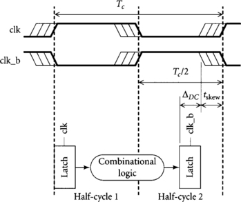
In the limit of long cycle time Tc, this approaches half a cycle. For shorter cycles, the clock skew and setup time overhead reduce the amount of available time borrowing.
If the latches are transparent for shorter amounts of time, the amount of time available for borrowing is reduced correspondingly. For example, in the next section we will discuss the possibility of using nonoverlapping clocks to avoid min-delay problems. The nonoverlap is subtracted from the amount of time available for borrowing. Similarly, pulsed latches can be viewed as transparent latches with short transparency windows. The amount of time borrowing supported by a transparent latch is therefore
If this amount is negative, the pulse width is too narrow to allow time borrowing. Of course, flip-flops permit no time borrowing because they impose hard edges.
Equations 2.5 and 2.6 show that there is a direct trade-off between time borrowing and clock skew. In effect, skew causes uncertainty in the arrival time of data. Budgeting for this uncertainty is just like budgeting for data intentionally being late on account of time borrowing. By more tightly bounding the amount of clock skew in a system, more time borrowing is possible.
Time borrowing may be used in several ways. Designers may intentionally borrow time to balance logic between slower and faster pipeline stages. The circuits will opportunistically borrow time after fabrication when manufacturing and environmental variations and inaccuracies in the analysis tools cause some delays to be faster and other delays to be shorter than the designer had predicted. While in principle designers could always repartition logic to balance delay as accurately as they can predict in advance and avoid intentional time borrowing, such repartitioning takes effort and increases time to market. Moreover, opportunistic time borrowing is always a benefit because it averages out uncertainties that are beyond the control of the designer and that would have otherwise limited cycle time.
A practical problem with time borrowing is that engineers faced with critical paths may assume they will be able to borrow time from an adjacent pipeline stage. Unfortunately, the engineer responsible for the adjacent stage may also have assumed that she could borrow time. When the pieces are put together and submitted for timing analysis, the circuit will be very far from meeting timing. This could be solved by good communication between designers, but because of trends toward enormous design teams and because of the poor documentation about such assumptions and the turnover among engineers, mistakes are often made. Design managers who have been burned by this problem in the past tend to forbid the use of time borrowing until very late in the design when all other solutions have failed. This is not to say that time borrowing is a bad thing; it simply must be used wisely.
2.2.4 Min-Delay
So far, we have focused on the question of max-delay: how long the cycle must be for each memory element to meet its setup time. The max-delay constraints set the performance of the system, but are relatively innocuous because if they are violated, the circuit can still be made to function correctly by reducing the clock frequency. In contrast, circuits also have min-delay constraints that memory element inputs must not change until a hold time after the sampling edge. If these constraints are violated, the circuit may sample the output while it is changing, leading to incorrect results. Min-delay violations are especially insidious because they cannot be fixed by changing the clock frequency. Therefore, the designer is forced to be conservative.
Figure 2.6 shows how min-delay problems can lead to incorrect operation of flip-flops. In the example, there are two back-to-back flip-flops with no logic between them. This is common in pipelined circuits where information such as an instruction opcode is carried from one pipeline stage to the next without modification as the instruction is processed. Suppose data input D1 is valid for a setup and hold time around the rising edge of clk, but that the propagation delay to Q1 is particularly short. Q1 is the input to the second flip-flop and changes before the end of the hold time for the second flip-flop. Therefore, the second flip-flop may incorrectly sample this new data and pass it on to Q2. In summary, the data that was at input D1 before the clock edge arrives at not only Q1 but also Q2 after the clock edge. This is referred to as double-clocking, a hold time or min-delay violation, or a race.
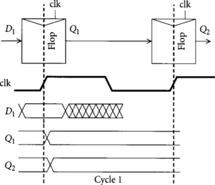
The term “min-delay” comes from the fact that the problem can be avoided by guaranteeing a minimum amount of delay between consecutive flip-flops. If there were more delay between the rising edge of the clock and the time data arrived at the second flip-flop, the hold time would not have been violated and the circuit would have worked correctly.
Min-delay problems are exacerbated by clock skew. If skew causes the clock of the first flip-flop to rise early, its output will become valid early. If skew then also causes the clock of the second flip-flop to rise late, its input will have to hold until a later time. Therefore, more delay is necessary between the flip-flops to ensure the hold time is not violated. Clock skew can be viewed as increasing the effective hold time of the second memory element.
We can guarantee that min-delay problems will never occur by checking a simple delay constraint between each pair of consecutive memory elements. Assume that data departs the first element as early as possible. Add the shortest possible delay between this departure time and the arrival at the second element; this is called the contamination delay. The arrival must be at least a hold time after the sampling edge of the second element, assuming maximum skew between the elements. To analyze our prospective latching techniques, we need a few more definitions. Let us define δCQ as the contamination delay of the memory element, that is, the minimum time from the clock switching until the output becoming valid. This is like δCQ but represents the minimum instead of maximum delay. Let δlogic be the contamination delay through the logic between the memory elements.
For flip-flops, data departs the first flip-flop on the rising edge of the clock. The flop and logic contamination delays must be adequate for the data to arrive at the second flip-flop after its hold time has elapsed, even budgeting clock skew:
Solving for the minimum logic contamination delay, we find
Notice that the constraint is independent of cycle time Tc. As expected, min-delay problems cannot be fixed by adjusting the cycle time.
For latches, data departs the first latch on the rising edge of one half-cycle. The latch and logic contamination delays must be sufficient for the data to arrive a hold time after the falling edge of the previous half-cycle.
Let us define tnonoverlap as the time from the falling edge of one half-cycle to the rising edge of the next. This time is typically 0 for complementary clocks, but may be positive for nonoverlapping clocks. The minimum logic contamination delay is
Notice that this minimum delay is through each half-cycle of logic. Therefore the full cycle requires minimum delay twice as great.
The following example may clarify the use of nonoverlapping clocks:
EXAMPLE 2.1
What is the logic contamination delay required in a system using transparent latches if the hold time is 0, the latch contamination delay is 0.5 FO4 inverter delays, the clock skew is 1 FO4 delay, and the nonoverlap is 2 FO4 delays, as shown in Figure 2.7?
SOLUTION
δlogic must be at least 0 + 1 – 0.5 – 2 = −1.5 FO4 delays. Because logic delays are always nonnegative, it is impossible for this system to experience min-delay problems.
Two-phase nonoverlapping clocking was once popular because of min-delay safety. It is still a good choice for student projects because it is completely safe; by using external control of the clock waveforms, the student can always provide enough nonoverlap and slow-enough clocks to avoid problems with either min-delay or max-delay. However, commercial high-speed designs seldom use nonoverlapping clocks because it is easier to distribute a single clock globally, and then locally invert it to obtain the two latch phases. Instead, the commercial designs check min-delay and insert buffers to increase delay in fast paths. Nonoverlapping clocks also reduce the possible amount of time borrowing. Note that there is a common fallacy that nonoverlapping clocks allow less time for useful computation. As can be seen from Figure 2.7, this is not the case; the full cycle less two latch delays is still available. The only penalty is the reduced opportunity for time borrowing.
For pulsed latches, data departs the first latch on the rising edge of the pulse. It must not arrive at the second pulsed latch until a hold time after the falling edge of the pulse. As usual, the presence of clock skews between the pulses increases the hold time. Therefore, the minimum contamination delay is
This is the largest required contamination delay of any latching scheme. It shows the trade-off that although wider pulses can hide more clock skew and even permit small amounts of time borrowing, the wide pulses increase the minimum amount of delay between latches. Adding this amount of delay between pulsed latches in cycles that perform no logic can take a significant amount of area. Therefore, systems that use pulsed latches for the critical paths that require low sequencing overhead sometimes also use flip-flops to reduce min-delay problems on paths that merely stage data along without processing.
You may have noticed that flip-flops and pulsed latches have a minimum delay per cycle, while transparent latches have a minimum delay per half-cycle, and hence about twice as much minimum delay per cycle. This may seem strange because flip-flops can be built from a pair of back-to-back transparent latches. Why should flip-flops have half the min-delay requirement as transparent latches if the systems have exactly the same building blocks? The answer is that flip-flops are usually constructed with zero skew between adjacent latches. By making the hold time ΔCD less than the contamination delay δDQ, the minimum logic delay between the two latches in the flip-flop is negative. If this were not the case, flip-flops would insidiously fail by sampling the input on the falling edge of the clock as well as the rising edge! We will revisit this issue while discussing flip-flop design in Section 2.3.3.
Min-delay can be enforced in many short paths by adding buffers. Long channel lengths are often used to make slower buffers so that fewer buffers are required. The hardest min-delay problems occur in paths that could be either fast or slow in a data-dependent fashion. For example, a path built from a series of NAND gates may be fast when both parallel PMOS transistors turn on and slower when only one PMOS transistor turns on. A path using wide domino OR gates is even more sensitive to input patterns. Therefore, circuit designers occasionally encounter paths that have both min- and max-delay problems. Because buffers cannot be added without exacerbating the max-delay problem, the circuits may have to be redesigned.
Min-delay requirements are easy to check because they only involve delays between pairs of consecutive memory elements. They are also conservative for systems that permit time borrowing because they assume data always departs the first latch at the earliest possible time. In a real system, time borrowing may cause data to depart the first latch somewhat later, making min-delay easier to satisfy. Unfortunately, if the real system is operated at reduced frequency, or at higher voltage where transistors are faster, data may again depart the first latch at the earliest possible time. Therefore, it is unwise to depend on data departing late to guarantee min-delay.
Because min-delay violations result in nonfunctional circuits at any operating frequency, it is necessary to be conservative when checking and guaranteeing hold times. Discovering min-delay problems after receiving chips back from fabrication is extremely expensive because the violation must be fixed and new chips must be built before the debugging of other problems such as long paths or logic errors can begin. This may add two to four months to the debug schedule in an industry with product cycles of two years or less.
2.3 Memory Element Design
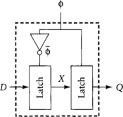
Now that we have discussed the performance of various memory elements, we will turn to the transistor-level implementations. Many transparent latch implementations have been proposed, but in practice a very old, simple design is generally best. Pulsed latches can be built from transparent latches with a brief clock pulse or may integrate pulsing circuitry into the latch. Flip-flops can be composed of back-to-back latches or of various precharged structures. We will begin by showing dynamic versions of the memory elements, and then discuss how to staticize the latches.
2.3.1 Transparent Latches
The simplest dynamic latch dating back to the days of NMOS is just a pass transistor, shown in Figure 2.8. Its output can only swing from 0 to VDD – Vt, where Vtis the threshold voltage of the transistor. To provide rail-to-rail output swings, a full transmission gate is usually a better choice.
Such latches have many drawbacks. The latch must drive only a capacitive load. If it drove the diffusion input of another pass transistor, when the latch is opaque and the pass transistor turns on, charge stored on the output node of the latch is shared between the capacitances on both sides of the pass transistor, causing a voltage droop. This effect is called charge sharing and can corrupt the result. Coupling onto the output node from adjacent wires is also a problem because the output is a dynamic node. Latch setup time depends on both the load and driving gate, just as the delay through an ordinary transmission gate depends on the driver and load. Therefore the latch is hard to use in a standard cell methodology that defines gate delays without reference to surrounding gates.
The setup time issue can be solved by placing an inverter on the input. Sometimes the inputs to the transmission gate are separated to create a tristate inverter instead, as shown in Figure 2.9. The performance of both designs is comparable; removing the shorting connection slightly reduces drive capability, but also reduces internal diffusion parasitics. Note that it is important for the clock input to be on the inside of the stack. If the data input were on the inside, changes in the data value while the latch was off could cause charge sharing and glitches on the output.
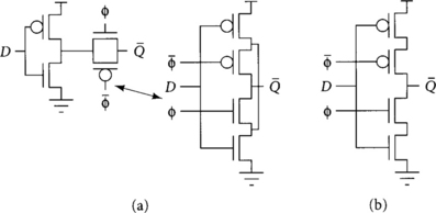
Placing an inverter on the output solves the charge-sharing problems and reduces noise coupling because the dynamic node is not routed over long distances.
To minimize clock skew, most chips distribute only a single clock signal across the entire chip. Locally, additional phases are derived as necessary. For example, an inverter may be used to create clk_b from clk. Once upon a time, some designers had only considered globally distributing the multiple phase. They correctly argued that such global distribution would lead to severe clock skew between the phases and high sequencing overhead [96]. Therefore, they recommended using as few clock phases as possible. This reasoning is faulty because local phase generators can provide many clock phases with relatively low skew. Nevertheless, it led to great interest in latching with only a single clock phase. Such true single-phase clocking (TSPC) latches are shown in Figure 2.10 as they compare to traditional latches with local phase generators.
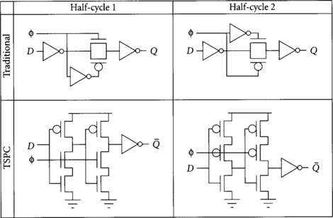
TSPC latches have a longer propagation delay because the data passes through more gates. As designers realized that inverting the clock can be done relatively cheaply and that TSPC latches are slower and larger than normal latches, TSPC latches fell from commercial favor. For example, the DEC Alpha 21064 used TSPC latches. A careful study after the project found that TSPC consumed 25% more area, presented 40% more clock load, and was 20% slower than traditional latches. Therefore, the Alpha 21164 returned to traditional latch design [26, 28].
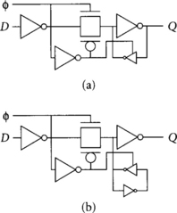
All latches that have been presented so far are dynamic; if left indefinitely, subthreshold conduction through the nominally OFF transistors may cause the gate to leak to an incorrect value. To allow a system to run at low frequency or with a stopped clock, the dynamic node must be staticized. This can be done with a weak feedback inverter or with a tristate feedback inverter. Weak inverter “jamb” latches introduce a ratio problem: the transistors in the forward path must be strong enough to overpower the feedback inverter over all values of PMOS-to-NMOS mobility ratios. Tristate inverters are thus safer and avoid contention power, but are larger. Feeding back from the output inverter is risky because noise on the output can overwrite the contents of the latch via the feedback gate while the latch is opaque. Thus, the output is often buffered with a separate gate, as shown in Figure 2.11. Staticizing TSPC latches is more cumbersome because there are multiple dynamic nodes.
The setup time ΔDC of the latch is the time required for data to propagate from the input to the dynamic node after the transmission gate so that when the clock falls, the new data sits on the dynamic node. The propagation delay ΔDQ is the time required for data to propagate from the input all the way to the output. The hold time ΔCD is zero or even negative in many latch implementations like those of Figure 2.11 because if data arrives at the input at the same time the clock falls, the transmission gate will be OFF by the time the data propagates through the input inverter.
In summary, for highest-performance custom design, a bare transmission gate is very fast and was used by DEC in the Alpha 21164. Care should be taken to compute the setup time as a function of the driver as well as the load capacitance. For synthesized design, an inverter/transmission gate/inverter combination latch is safer to guarantee setup times and safety of the dynamic node. In any case, designs that must support stop clock or low-frequency operation should staticize the dynamic node with a feedback gate.
2.3.2 Pulsed Latches
In principle, a pulsed latch is identical to a transparent latch, but receives a narrow clock pulse instead of a 50% duty cycle clock [89]. The key challenge to pulsed latches is generating and distributing a pulse that is wide enough for correct operation but not so wide that it causes terrible min-delay problems. Unfortunately, pulse generators are subject to variation in transistor parameters and operating conditions that may narrow or widen the pulse. If you do not remember that setup times will also get shorter as transistors become faster and pulses narrow, you may conclude it is virtually impossible to design a reasonable pulse generator. Commercial processors have proved that the concept can work, though we will see in the historical perspective that these processors have had production problems that might be attributed to risky circuit techniques. Because it is extremely difficult to propagate narrow pulses cleanly across long lossy wires, we will assume the pulses must be generated locally.
The conceptually simplest pulsed latch is shown in Figure 2.12. The left portion is called a clock chopper, pulse generator, or one-shot; it produces a short pulse ϕp on the rising clock edge. The clock chopper can serve a single latch or may locally produce clocks for a small bank of latches. The latch is shown in dynamic form without an output inverter, but can be modified to be static and have better noise immunity just like a transparent latch. Indeed, any transparent latch, including unbuffered transmission gates and TSPC latches, may be pulsed.
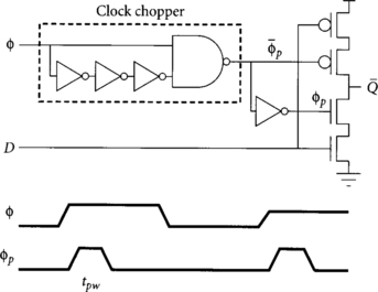
It is difficult to generate very narrow pulses with a clock chopper because of the finite rise and fall times, so shorter pulses are often constructed from the intersection of two wider pulses. The Partovi pulsed latch [64] of Figure 2.13 integrates the pulse generator into the latch to achieve narrower pulses in just this way at the expense of greater ΔDQ propagation delay. The latch was originally called a “hybrid latch-flip-flop” (HLFF) because it was intended to replace a flip-flop. However, calling it a flip-flop is misleading because it is not strictly edge-triggered.
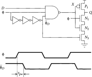
When the clock is low, the delayed clock ![]() is initially high and node X is set high. The output Q floats at its old value. When the clock rises, both
is initially high and node X is set high. The output Q floats at its old value. When the clock rises, both ![]() and
and ![]() are briefly high before
are briefly high before ![]() falls. During this overlap, the latch is transparent. The NAND gate acts as an inverter, passing X =
falls. During this overlap, the latch is transparent. The NAND gate acts as an inverter, passing X = ![]() because the other two inputs are high. The final gate also acts as an inverter because transistors N1 and N3 are high. Therefore, the latch acts as a buffer while transparent. When
because the other two inputs are high. The final gate also acts as an inverter because transistors N1 and N3 are high. Therefore, the latch acts as a buffer while transparent. When ![]() falls, the pulldown stacks of the NAND gate and the final gate both turn off. This cuts output node Q off from the input D, leaving the latch in an opaque mode. As usual, the latch can be made static by placing cross-coupled inverters on the output.
falls, the pulldown stacks of the NAND gate and the final gate both turn off. This cuts output node Q off from the input D, leaving the latch in an opaque mode. As usual, the latch can be made static by placing cross-coupled inverters on the output.
We will return to pulsed latch variants in Section 4.1.2, when we study the static-to-domino interface.
2.3.3 Flip-Flops
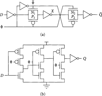
A flip-flop can be constructed from two back-to-back transparent latches, as shown in Figure 2.14. When the clock is low, the first latch is transparent and the second latch is opaque. Therefore, data will advance to the internal node X. When the clock rises, the first latch will become opaque, blocking new inputs, and the second latch will become transparent. The flip-flop setup time is the setup time of the first latch. The clock-to-Q delay is the time from when data is at the dynamic node of the first latch and the clock rises until the data reaches the output of the flip-flop. It is therefore apparent that the sum of the setup and clock-to-Q delays of the flip-flop is equal to the sum of the propagation delays through the latches because in both cases the data must pass through two latches. Combining this observation with Equations 2.2 and 2.3, we see that the overhead of a flip-flop system is worse than that of a transparent latch system by the clock skew.
In practice, the latches used in flip-flops can be slightly simpler than those used in stand-alone applications because the internal node X is protected and does not need all the buffering of two connected latches. Figure 2.15 shows such optimized flip-flops built from transmission gate latches and from TSPC latches.
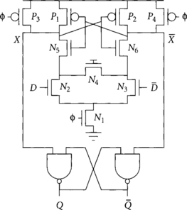
Remember that the skew between back-to-back latches of a flip-flop must be small or the flip-flop may have an internal min-delay problem. This problem is illustrated in Figure 2.16. Suppose that ϕ is badly skewed relative to ϕ, possibly because the local inverter is undersized and thus too slow. When the clock falls, both transistors P1 and P2 of Figure 2.15 will be simultaneously on for a brief period of time. This allows data to pass from D to Q during this time, effectively sampling the input on the falling edge of the clock. The problem can be avoided by ensuring that the ![]() inverter is fast enough to turn off P2 before new data arrives. TSPC latches are immune to this problem because they only use one clock, but are susceptible to internal races when the clock slope is very slow, causing both NMOS and PMOS clocked transistors to be on simultaneously during the transition. A modified traditional flip-flop design based on tristate latches instead of transmission gate latches shown in Figure 2.17 [24] also avoids internal races because data will pass through the NMOS transistors of one tristate and the PMOS transistors of the other tristate, never through the PMOS transistors of both stages. Of course, while avoiding internal races is necessary, it does not eliminate the problem of min-delay between flip-flops.
inverter is fast enough to turn off P2 before new data arrives. TSPC latches are immune to this problem because they only use one clock, but are susceptible to internal races when the clock slope is very slow, causing both NMOS and PMOS clocked transistors to be on simultaneously during the transition. A modified traditional flip-flop design based on tristate latches instead of transmission gate latches shown in Figure 2.17 [24] also avoids internal races because data will pass through the NMOS transistors of one tristate and the PMOS transistors of the other tristate, never through the PMOS transistors of both stages. Of course, while avoiding internal races is necessary, it does not eliminate the problem of min-delay between flip-flops.
The traditional flip-flop can be made static by adding feedback onto the dynamic nodes after each of the two transmission gates. This would be very costly in the TSPC flip-flop for three reasons: (1) the presence of three dynamic nodes instead of just two, (2) the lack of an inverted version of each node to feed back, and (3) the lack of a complementary clock to operate a transmission gate.
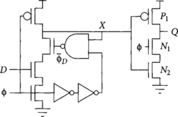
The Klass semidynamic flip-flop (SDFF) [47, 48] of Figure 2.18 is based on a different idea. Like the Partovi pulsed latch, it operates on the principle of intersecting pulses. Compared to the Partovi latch, it may have a slightly shorter propagation delay, but is edge-triggered and thus loses the skew tolerance and time-borrowing capabilities of pulsed latches. The Klass SDFF replaces the static NAND gate of the Partovi pulsed latch of Figure 2.13 with a dynamic NAND. Because node X is guaranteed to be monotonically falling while the clock is high, the output stage can also be simplified by removing N3· Another modification is that ![]() is gated by X. If D is low,
is gated by X. If D is low, ![]() will fall three gate delays after the clock rises, providing a very narrow pulse. If D is high, X will start to pull down and
will fall three gate delays after the clock rises, providing a very narrow pulse. If D is high, X will start to pull down and ![]() will not fall. This allows more time for X to fall all the way and purportedly permits a narrower pulse than would be possible if X had to pull from high all the way low during the pulse. Another advantage is that fast, relatively complex logic can be built into the first stage, which behaves as a dynamic gate. The latch needs cross-coupled inverters on both X and Q for fully static operation. A drawback relative to ordinary flip-flops is that, like a pulsed latch, the hold time is increased by the pulse width.
will not fall. This allows more time for X to fall all the way and purportedly permits a narrower pulse than would be possible if X had to pull from high all the way low during the pulse. Another advantage is that fast, relatively complex logic can be built into the first stage, which behaves as a dynamic gate. The latch needs cross-coupled inverters on both X and Q for fully static operation. A drawback relative to ordinary flip-flops is that, like a pulsed latch, the hold time is increased by the pulse width.
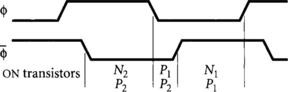
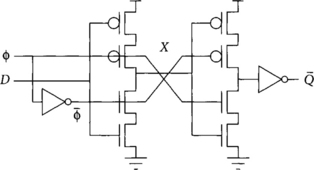
Yet another flip-flop design is the sense-amplifier flip-flop (SAFF) [28, 55, 58] of Figure 2.19, which has been used in the Alpha 21264 and in the StrongARM. The flip-flop requires differential inputs and produces a differential output. It can be understood as a dual-rail domino buffer with regenerative feedback followed by an SR latch on the output to retain the output state during precharge. Remarkably, a single transistor N4 serves to staticize the latch; this transistor can be omitted in dynamic implementations.
When the clock is low, evaluation transistor N1 is off and precharge transistors P3 and P4 pull the internal nodes X and ![]() high. When the clock rises, one of the inputs will be at a higher voltage than another. This will cause the corresponding node X or
high. When the clock rises, one of the inputs will be at a higher voltage than another. This will cause the corresponding node X or ![]() to pull down. Transistors P1, P2, N5, and N6 together form a cross-coupled inverter pair that performs regenerative feedback to amplify the difference between X and
to pull down. Transistors P1, P2, N5, and N6 together form a cross-coupled inverter pair that performs regenerative feedback to amplify the difference between X and ![]() . Initially both N5 and N6 are on, allowing either side to pull low. As one side pulls down, the NMOS transistor on the other side begins to turn off and the PMOS transistor begins to turn on, holding the other side high. Once one side has fully pulled down, the flip-flop ceases to respond to input changes so the hold time is quite short. If the input changes, the internal nodes may be left floating unless weak staticizer N4 is available to provide a trickle of current. When the clock falls, the internal nodes precharge but the cross-coupled nand gates on the output serve as an SR latch to retain the value.
. Initially both N5 and N6 are on, allowing either side to pull low. As one side pulls down, the NMOS transistor on the other side begins to turn off and the PMOS transistor begins to turn on, holding the other side high. Once one side has fully pulled down, the flip-flop ceases to respond to input changes so the hold time is quite short. If the input changes, the internal nodes may be left floating unless weak staticizer N4 is available to provide a trickle of current. When the clock falls, the internal nodes precharge but the cross-coupled nand gates on the output serve as an SR latch to retain the value.
As a general-purpose flip-flop, the SAFF is not very fast. One of the internal nodes must first pull down, causing one of the outputs to rise, then the other output to fall, leading to three gate delays through the flop. However, the SAFF has other advantages. It is used in the Alpha 21264 to amplify 200 mV signal swings [22] from the register file and on other heavily loaded internal busses, greatly reducing the delay of the input swing. Because the core of the flop is just a dual-rail domino gate, it is easy to build logic into the gate for greater speed. Care must be taken, however, when incorporating logic to avoid charge-sharing noise that incorrectly trips the sense amplifier. Finally, when the flip-flop interfaces to domino logic, the SR latch can be removed because the domino logic does not need inputs to remain stable all cycle. In summary, the SAFF is a good choice for certain applications where its unique features are beneficial.
Stojanovic and Oklobdzija made a thorough study of flip-flop variants [81]. The study focused on the power-delay product rather than the delay given fixed input and output capacitance specifications. It found the Klass SDFF to be the fastest, while the traditional flip-flop built from two transparent latches offered the lowest power-delay product.
2.4 Historical Perspective
The microprocessor industry has experienced a fascinating evolution of latching strategies. Digital Equipment Corporation (now part of Compaq) took the microprocessor industry by surprise by developing the 200 MHz Alpha 21064 in 1992 [16], when most other microprocessors were well below 100 MHz. At that time, designers strove to distribute the clock on a single wire to nearly all latches and to avoid completely the need for checking min-delay problems with inadequate tools. They therefore challenged the conventional wisdom by using TSPC latches instead of traditional latches or flip-flops. As we have seen, TSPC proved a poor choice, requiring more area and clock power and being slower than regular transparent latches. Therefore, the Alpha 21164 returned to static latches [26]. They gained speed by using a bare transmission gate as the basic latch and choosing from a characterized library of simple gates at the input and output of the transmission gate. This allowed designers to build logic into the latch and minimize the sequencing overhead. At least one logic gate was required between each latch to avoid min-delay problems. Curiously, the Alpha 21264 began using a family of edge-triggered flip-flops [28]; overhead was tolerable because great effort went into the clock distribution system.
Interestingly, the 21064 and 21164 employed dynamic latches to avoid the extra delay of staticizers. To retain dynamic state, the processors had a minimum clocking frequency requirement as high as 1/10 of the maximum frequency [26]. This made testing and debug more challenging and is not a viable option for processors targeting laptop computers and other machines that need a low-power sleep mode. The 21264 used static memory elements because it required clock gating to keep power under control by turning off unused elements.
Unger has done a thorough, though dense, analysis of the overhead and clocking requirements of flip-flops, transparent latches, and pulsed latches [89]. Transparent latches are used in many machines. For example, IBM has been a longtime user, extensively employing a Level-Sensitive Scan Design methodology (LSSD) with transparent latches [15, 75]. Motorola uses a similar methodology on PowerPC microprocessors [2]. Silicon Graphics mixed transparent latches in speed-critical sections with flip-flops in noncritical sections on the R1000. Pulsed latches were once deemed too risky for commercial microprocessors, but have come into favor recently among some aggressive designers. AMD used the Partovi pulsed latch in the K6 microprocessor [64].
It will be interesting to watch how latches evolve in the future. As recently as 1993, some authors predicted the exclusive use of single-phase clocking [92]; that has not come true for high-performance systems. Despite the host of new latches proposed by academics [24, 96, 97], simple transparent latches and pulsed latches are likely to vie for the lead on high-speed designs, while flip-flops will be used extensively where sequencing overhead is less important.
2.5 Summary
In this chapter we have explored the commonly used memory elements for static circuits: flip-flops, transparent latches, and pulsed latches. Transparent latches can be viewed as the basic element; a flip-flop is composed of a pair of transparent latches receiving complementary clocks, while a pulsed latch is a single transparent latch receiving a pulsed clock. Table 2.1 summarizes the performance of each type of memory element. Flip-flops are the slowest. Transparent latches are good for skew-tolerant circuit design because they can hide nearly half a cycle of clock skew and permit plenty of time borrowing. Pulsed latches have the lowest sequencing overhead of any latch type, but handle less skew and time borrowing and require the most attention to min-delay problems.
Pulsed latches are a good option for high-performance designs when skews are tightly controlled and min-delay tools are good. They are conceptually simple and compatible with most design flows because they are placed in the cycle in just the same way as flip-flops. Transparent latches are another good option for high-performance design when clock skews are more significant, time borrowing is necessary to balance logic, or the min-delay checks are inadequate. Thus, the choice between pulsed latches and transparent latches is more a matter of designer experience and judgment than of compelling theoretical advantage. Flip-flops are the slowest solution and should be reserved for systems where sequencing overhead is a minor portion of the cycle time.
The traditional pass-gate latch implementations are fast and reasonably compact. TSPC latches only require a single clock phase, but this is an illusory benefit: ultimately the designer cares about the performance, area, and power of the complete system. The extra stages and transistors in the TSPC design make it slower and more costly, so traditional designs continue to be prevalent.
2.6 Exercises
[15] 2.1. In your own words, define static and dynamic circuit families and static and dynamic memory elements. What is the difference in the usage of the words “static” and “dynamic” as applied to circuit families versus memory elements?
[20] 2.2. Consider a system with a target cycle time of 1 GHz. The clock skew budget is 150 ps. You are considering using flip-flops, transparent latches, or pulsed latches as the memory elements. How much time is available for logic within the cycle for each of the following scenarios?
(a) Flip-flops: setup time = 90 ps; clock-to-Q delay = 90 ps; hold time = 20 ps; contamination delay = 40 ps
(b) Transparent latches: setup time = 90 ps; clock-to-Q delay = 90 ps; D-to-Q delay = 70 ps; hold time = 20 ps; contamination delay = 40 ps
(c) Pulsed latches: setup time = 90 ps; clock-to-Q delay = 90 ps; D-to-Q delay = 70 ps; hold time = 20 ps; contamination delay = 40 ps. Consider using pulse widths of 180 ps and 250 ps.
[25] 2.3. Consider the paths in Figure 2.20. Using the data from Exercise 2.2, compute the following minimum and maximum delays:
(b) Transparent latches: Assuming 50% duty cycle clocks, compute maximum values of Δ1, Δ2, and Δ1 + Δ2; and minimum values of δ1, δ2, and δ1 + δ2. Remember to allow for time borrowing.
(c) Pulsed latches: Δ1, δ1 Consider using pulse widths of 180 ps and 250 ps.
[20] 2.4. Repeat part (b) of Exercise 2.3 if the duty cycle of each latch clock is d, where d is in the range of 0.3 to 0.7. Remember that the duty cycle of the clock is the fraction of time it is high. Duty cycles less than 0.5 imply nonoverlapping clocks, as shown in Figure 2.21, while duty cycles greater than 50% imply overlapping clocks.
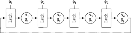
[25] 2.5. Using the data from Exercise 2.2, compute the maximum values of Δ1, Δ2, Δ3, Δ4, Δ1 + Δ2, Δ2 + Δ3, Δ1+ Δ2 + Δ3, and Δ1+ Δ2 + Δ3 + Δ4 for the circuit in Figure 2.22. Assume 50% duty cycle clocks. Remember to allow for time borrowing.
[10] 2.6. What are the advantages of using wide pulses for pulsed latches? What are the disadvantages of wide pulses?
[30] 2.7. Simulate the traditional static latch of Figure 2.10 in your process. Use an identical latch as the load. Make a plot of the D-to-Q delay as a function of the time from the changing data input to the falling edge of the clock. From this plot, determine the D-to-Q and setup times of the latch. Comment on how you define each of these delays.
[30] 2.8. Extend your simulation from Exercise 2.7 to determine the hold time of the latch. How do you define and measure hold time?