
Circuit Methodology

In this chapter, we will develop a skew-tolerant circuit design methodology. There are many aspects to skew-tolerant circuit design, including the interface of static and domino logic, clocking, and testability. Unless you consider all aspects simultaneously, it is easy to optimize one aspect at the expense of the others, resulting in a system that is slower overall or more difficult to build. Our objective is a coherent approach to combine domino gates, transparent latches, and pulsed latches, while providing simple clocking, easy testability, and robust operation. The guidelines presented are self-consistent and support the design and verification of fast systems, but are not the only reasonable choices.
Our design methodology contains definitions and guidelines. Definitions provide a common set of terms that enable tools to parse the design. Guidelines should be followed for easy, robust design. They should only be violated after being fully understood. During a design review, guideline violations should be discussed.
We will emphasize circuit design in this chapter while deferring discussion of the clock network until the next chapter. Of course, circuit design and clocking are intimately related, so this methodology must make assumptions about the clocking. In particular, we assume that we are provided four overlapping clock phases with 50% duty cycles. These clocks will be used for both skew-tolerant domino and static latches.
DEFINITION 1
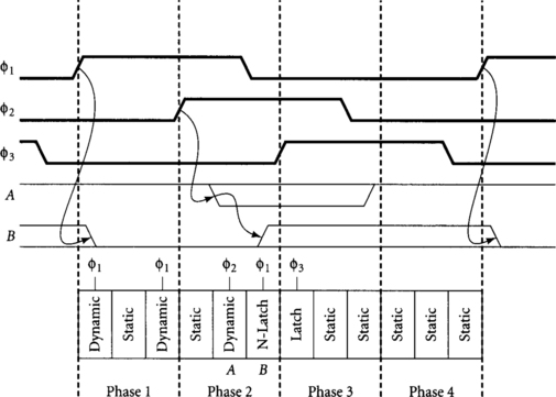
The clocks are named φ1, φ2, φ3, and φ4. Their nominal waveforms are shown in Figure 4.1.
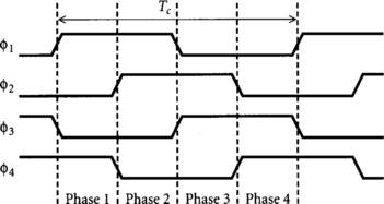
The clocks are locally generated from a single global clock gclk. φ1 and φ3 are logically true and complementary versions of gclk. φ2 and φ4 are versions of φ1, and φ3 nominally delayed by a quarter cycle. The clocks may be operated at reduced frequency or may even be stopped while gclk is low for testability or to save power.
The methodology primarily supports four-phase skew-tolerant domino, pulsed latches, and φ1 and φ3 transparent latches. Other latch phases are occasionally used when interfacing static and domino logic. It is recommended, but not required, that you choose either transparent latches or pulsed latches as the primary static latch to simplify design.
4.1 Static/Domino Interface
In the previous chapters, we have analyzed systems built from static CMOS latches and logic and systems built from skew-tolerant domino. In this section, we discuss how to interface static logic into domino paths and domino results back into static logic. We focus on static logic using transparent latches and pulsed latches because flip-flops are not tolerant of skew. We develop a set of “timing types” that determine when signals are valid and allow checking that circuits are correctly connected. The guidelines emphasize performance at the cost of checking min-delay conditions.
4.1.1 Latch Placement
Before discussing the static/domino interface, we must decide where static latches belong in the cycle. Of course, pulsed latches are placed at the beginning of a cycle when the pulse occurs and domino gates are assigned to nominally evaluate during one of the four phases. Transparent latches pose a dilemma, however: should they be placed at the beginning, middle, or end of their half-cycle? We will look at each option, then conclude that placement scarcely matters in latch-based loops because the latches adjust themselves as early as possible in the cycle depending on data arrival times. Therefore, we might as well nominally place the latch at the beginning of the cycle.
In Section 1.3, we argued that latches could tolerate clock skew if they were placed in the middle of their half-cycle such that skew disturbing the latch transparency at the beginning or end of the half-cycle has no effect. Placing latches in the middle of the half-cycle presents two difficulties.
One is that the designer must determine where the “middle” is in a half-cycle of logic. Another is that designers often construct logic with a minimum number of signals crossing cycle boundaries because the cycle boundaries also represent partitions of a large system between modules and designers. Within the cycle, a larger number of intermediate results may be generated. If latches were placed in the middle of a half-cycle, more latches might be required.
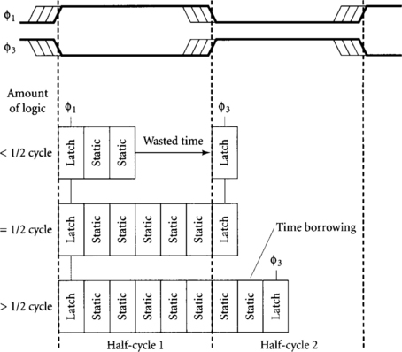
The alternatives are to place latches at the beginning or end of each half-cycle. Designers who are accustomed to thinking about latches as memory elements often like to place the latch at the end of the half-cycle [66] to “remember” the result of the computation in the half-cycle. Recall, however, from Section 2.1.1 that the purpose of a latch is not to remember information but rather to retard fast signals from racing ahead and corrupting information in the next cycle. Fast signals arrive early, so the function of a latch is to remain opaque until the signals are allowed to enter the half-cycle. From this point of view, it makes sense for latches to be placed at the beginning of the half-cycle. Data that is not critical arrives at the latch before it becomes transparent. Time borrowing occurs when data arrives late and propagates through the latch while it is transparent. This is exactly the behavior observed when using a functional simulator that assumes zero delay through gates. Thinking of latches as belonging at the beginning of half-cycles is also convenient because it emphasizes the similarities of transparent latches and pulsed latches, works well with scan (Section 4.3), and matches the results of timing analysis (Chapter 6).
At first glance, it appears wasteful for data to nominally arrive at a latch while the latch is still opaque. The data will be delayed waiting for the latch to become transparent. Does this introduce sequencing overhead? Interestingly, the answer is no. Noncritical signals do arrive before the latch is transparent and are slowed to stay synchronized. Critical signals, however, are late and thus arrive while the latch is transparent. For example, Figure 4.2 shows the arrival times of noncritical and critical signals. We assume paths starting from the φ1 latch depart at the latest the latch might become transparent in the event of clock skew. The top path is less than a half-cycle, so it must wait for the φ3 latch to become transparent. This introduces sequencing overhead but is unimportant because the path was faster than necessary. The middle path is exactly a half-cycle, so it arrives at the φ3 latch just as the latch has become transparent. Therefore, no time is wasted. The bottom path is more than a half-cycle, so it borrows time into the second half-cycle. This time borrowing effectively pushes the φ3 latch later into the second half-cycle. The maximum amount of time borrowing is set by the fact that data must arrive at the latch by a setup time before the earliest skewed falling edge of the clock. In summary, we can think of latches being nominally placed at the beginning of each half-cycle. Critical paths incur no overhead from clock skew or setup time. Time borrowing can push the actual location of the latch further into the half-cycle.
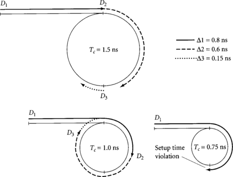
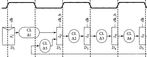
Even if latches were placed somewhere other than the beginning of a half-cycle, during operation they adjust themselves so that data arrives before the latch becomes transparent unless the logic is slow enough that time borrowing is necessary. For example, Figure 4.3 illustrates a path consisting of a loop through two latches L2 and L3. The loop also receives an external input from a flip-flop F1. The propagation delays through the combinational logic (CL) are Δ1, Δ2, and Δ3. The departure times from each element, that is, the time at which data begins propagating through the latch, are D1, D2, and D3. The latches are nominally placed at the end of the half-cycles in the pipeline diagram, but we will see that if the combinational logic delays are short compared to the cycle time, data will arrive at latches before they become transparent, so the latches will effectively operate at the beginning of the half-cycles.
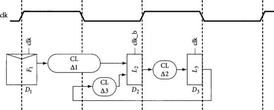
Figure 4.4 illustrates the circuit timing assuming Δ1 = 0.2 ns, Δ2 = 0.6 ns, and Δ3 = 0.15 ns. The three diagrams correspond to cycle times Tc of 1.5 ns, 1.0 ns, and 0.75 ns. The vertical tic marks delineate half-cycle boundaries. The loop formed by the two latches is rolled into a circle; the circumference of the circle represents the cycle time. The external input from the flip-flop is represented by the horizontal line. The heavy lines correspond to times when blocks of combinational logic are operating and the departure times from each latch are indicated on the diagram. In each case, data departs the flip-flop on the rising edge of the clock. When the cycle time is 1.5 ns, data arrives at the input of each latch before the latch becomes transparent. Therefore, the data departs the latch at the beginning of the half-cycle when the latch becomes transparent, even though the pipeline diagram had planned latches at the end of the half-cycle. When the cycle time drops to 1.0 ns, Δ2 exceeds half of the cycle time, so data departs L3 after the clock edge. This indicates that time borrowing is taking place. When the cycle time drops to 0.75 ns, even more time borrowing is required. The arcs formed by Δ2 and Δ3 sum to the entire circumference of the circle, indicating that the system is operating at the minimum possible cycle time.
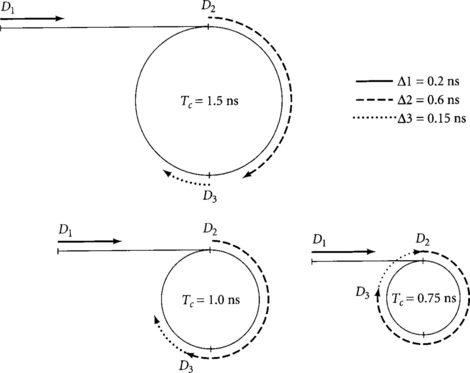
Figure 4.5 is a similar diagram showing how operation changes when Δ1 increases to 0.8 ns. Even when the cycle time is 1.5 ns, Δ1 is so long that data does not depart L2 until after the clock edge. The hard edge imposed by the flip-flop determines the departure time from the latch. Δ2 is short enough, however, that no time borrowing is required through L3. When the cycle time drops to 1.0 ns, time borrowing is required through both latches. At a cycle time of 0.75 ns, Δ1 is longer than a cycle and the setup time at L2 is violated. Therefore, the circuit will not operate, even though the delay around the loop Δ2 + Δ3 exactly fits in the cycle time.
In summary, loops of logic and transparent latches automatically adjust themselves so that data departs the latches at the beginning of each half-cycle unless time borrowing is necessary. Long paths from other latches or from elements like flip-flops or domino gates that impose hard edges may require time borrowing and thus dictate departure times. For the purpose of design, it suffices to nominally position latches at the beginning of the half-cycle; in the event of clock skew, data will automatically adjust using time borrowing to allow the system to operate at its minimum cycle time.
4.1.2 Static-to-Domino Interface
When nonmonotonic static signals are inputs to domino gates, they must be latched so that they will not change while the domino gate is in evaluation. The interface also imposes a hard edge because the data must set up at the domino input before the earliest the domino gate might begin evaluation, but may not propagate through the domino gate until the latest the gate could begin evaluation. Therefore, clock skew must be budgeted at the static-to-domino interface. This skew budget can be minimized by keeping the path in a local clock domain; Section 6.3 computes how much skew must be budgeted. Note that, strictly speaking, only falling inputs to domino gates must set up before evaluation. If your timing analyzer separately tracks arrival times for rising and falling edges, you can relax the constraints on the rising edge.
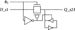
The latching technique at the interface depends on whether transparent or pulsed latches are used. In systems using transparent latches, static logic from one half-cycle can directly interface to dynamic logic at the start of the next half-cycle. The static outputs will not change while the domino is in evaluation. In systems with pulsed latches, however, the pulsed latch output may change while φ1 domino gates are evaluating. Therefore, a modified pulsed latch must be used at the interface to produce monotonic outputs. This is called a “pulsed domino latch” [43] and is shown in Figure 4.6.
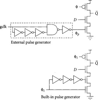
The pulsed domino latch essentially consists of a domino gate with a pulsed evaluation clock. The pulse may either be generated externally or produced by two series evaluation transistors as shown in the figure. The former scheme yields a faster latch because fewer series transistors are necessary, but requires longer pulses, as was discussed for ordinary pulsed latches in Section 2.3.2. Logic functions may be built into the pulsed domino latch.
The output of a static pulsed latch may be connected through static logic to φ2 or φ3 domino gates, so long as the static result settles before the domino enters evaluation. Master-slave flip-flops can be interfaced the same way. Neither static pulsed latches nor flip-flops directly interlace to φ1 domino gates because the output is not monotonic during φ1.
4.1.3 Domino-to-Static Interface
While a signal propagates through a skew-tolerant domino path, latches are unnecessary. However, before a domino output is sent into a block of static logic, it must be latched so that the result is not lost when the domino gate precharges. We will use a special latch at this interface that takes advantage of the monotonic nature of the domino outputs to improve performance.
Figure 4.7 shows the interface from domino to static logic. The dynamic gate drives a special latch using a single clocked NMOS transistor. This latch is called an N-C2MOS stage by Yuan and Svensson [96]; we will sometimes abbreviate it as an N-latch. When the dynamic gate evaluates, its falling transition propagates very quickly through the single PMOS transistor in the N-C2MOS latch. When the dynamic gate precharges and its output rises, the latch turns opaque, holding the value until the next time the clock rises. A weak keeper improves noise immunity when the clock is high. It is important to minimize the skew between the dynamic gate and N-C2MOS latch so that precharge cannot ripple through the latch. This is easy to do by locating the two cells adjacent to one another sharing the same clock wire. In Section 4.1.4, we will avoid this race entirely by using a latch clock that falls before the dynamic gate begins precharge. The only overhead at the interface from dynamic to static logic is the latch propagation delay.
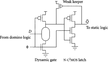
The output Q of the circuit will always fall when the clock rises, then may rise depending on the input D. This results in glitches propagating through the static logic when D is held at a logic for multiple cycles; the glitches lead to excess power dissipation. When dual-rail domino signals are available, an SR latch can be used at the domino-to-static interface, as shown in Figure 4.8. The SR latch avoids glitches when the domino inputs do not change, but is slower because results must propagate through two NAND gates.

A regular transparent latch also can be used at the domino-to-static interface, but is slower than the n-c2mos latch and has the same glitch problems.
4.1.4 Timing Types
The rules for connecting domino and static gates are complex enough that it is worthwhile systematically defining and checking the legal connectivity. To do this, we can generalize the two-phase clocking discipline rules of Noice [61] to handle four-phase skew-tolerant domino. Each signal name is assigned a suffix describing its timing. Proper connections can be verified by examining the suffixes. We first review the classical definition of timing types in the context of two-phase nonoverlapping clocks. Most systems use 50% duty cycle clocks, so we describe how timing types apply to such systems at the expense of checking min-delay. We then generalize timing types to four-phase skew-tolerant domino, including systems that mix domino, transparent latches, and pulsed latches. Timing types also include information about monotonicity and polarity to describe domino and dual-rail domino logic.
Two-Phase Nonoverlapping Clocks
Systems constructed from two-phase nonoverlapping clocks and φ2, like the one we examined in Figure 2.7, have the pleasant property that as long as simple topological rules are obeyed, the system will have no setup or hold time problems if run slowly enough with sufficient nonoverlap, regardless of clock skew [29]. They are particularly popular in student projects because no timing analysis is necessary. Timing types are used to specify the topological rules required for correct operation and allow automatic checking of legal connectivity. In later sections, we will extend timing types to work with practical systems that do not have nonoverlapping clocks. The extension comes at the expense of checking min-delay violations.
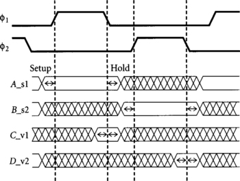
Each signal is given a suffix indicating the timing type and phase. The suffixes are _s1, _s2, _v1, _v2, _q1, and _q2. _s indicates that a signal is stable during a particular phase; that is, that the signal settles before the rising edge of the phase and does not change until after the falling edge. _v means that the signal is valid for sampling during a phase; it is stable for some setup and hold time around the falling edge of the phase. _q indicates a qualified clock, a glitch-free clock signal that may only rise on certain cycles. These timing types denote which clock edge controls the stability regions of the signals, that is, when the circuit is operated at slow speed, after which edge does the signal settle. Figure 4.9 shows examples of stable and valid signals. Stable is a stronger condition than valid; any stable signal can be used where a valid signal is required.
From the previous definitions, we see that clocks are neither valid nor stable. They establish the time and sequence references for data signals and are never latched by other clocks. However, it is sometimes useful to provide a clock that only pulses on certain cycles. _q indicates that the signal is such a qualified clock, a clock gated by some control so that it may not rise during certain cycles. Clock qualification is discussed further in Section 4.1.5. Qualified clocks are interchangeable with normal clocks for the purpose of analysis.
The inputs to latches must be valid for a setup and hold time around the sampling edge of the latch clock. For the purpose of verifying correct operation with timing types, it is helpful to imagine operating the system at low frequency so all latch inputs arrive before the rising edge of the clock and no time borrowing is necessary. Thus, a latch output will settle sometime after the rising edge of the latch clock and will not change again until the following rising edge of the latch clock; hence it is stable throughout the other phase. If the system operates correctly at low speed, we can then increase the clock frequency, borrowing time until setup times no longer are met.
In summary, a (φ1 latch requires a _vl or _sl input and produces a _s2 output. A φ2 latch requires a _v2 or _s2 input and produces a _s1 output. Combinational logic does not change timing types because the system can be operated slowly enough that data is still valid or stable in the specified phase. Figure 4.10 illustrates a general two-phase system.
Valid signals are produced by domino gates, as shown in Figure 4.11. The outputs settle sometime after the rising edge of the clock and do not precharge until the rising edge of the next clock, so they are valid for sampling around the falling edge of the clock. Using different precharge and evaluation clocks avoids any races between precharge and sampling. We also tag domino signals as monotonically rising (r) or falling (f). Domino inputs must be either stable or valid and monotonically rising during the phase the gate evaluates. The output of the dynamic gate is monotonically falling, and the output of the inverting static gate is monotonically rising. In such a traditional domino clocking scheme, the nonoverlap also appears as sequencing overhead.
As long as systems using two-phase nonoverlapping clocks have inputs to domino and latches using the proper timing types summarized in Table 4.1, the systems will always function at some speed. Setup time violations caused by long paths or excessive skew are solved by increasing the clock period. Hold time violations caused by short paths or excessive skew are solved by increasing the nonoverlap between phases.
Most two-phase systems use 50% duty cycle clocks rather than nonoverlapping clocks. Timing types are still useful to describe legal connectivity, but clock skew can lead to hold time failures that cannot be fixed by slowing the clock. Therefore, such systems must be checked for min-delay. In essence, the definitions of _v and _s must change to reflect the fact that the user can no longer control how long a signal will remain constant after the falling edge of a sampling clock. Also, since the two clocks are now complementary, domino gates use the same clock for evaluation and precharge. This leads to another hold time race as domino gates precharge at the same time as the latch samples. Timing types are still useful to indicate legal inputs to dynamic gates and transparent latches, but no longer guarantee immunity to min-delay problems.
Four-Phase Skew-Tolerant Domino
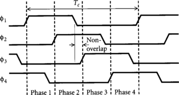
We can generalize the idea of timing types to four-phase skew-tolerant domino. Again, we will construct timing rules assuming that duty cycles can be adjusted to eliminate min-delay problems. Specifically, to avoid min-delay problems, each phase overlaps the next, but nonadjacent phases must not overlap, as shown in Figure 4.12. For example, φ1 and φ3 are nonoverlapping. In Section 4.1.6 we will consider the min-delay races that must be checked when the nonadjacent phases may overlap. We also use timing types to describe the interface of four-phase skew-tolerant domino with transparent latches, pulsed latches, and N-C2MOS latches.
GUIDELINE 1
Each signal name must have a suffix that describes the timing, phase, monotonicity, and polarity.
The timing is s, v, or q and the phase is 1, 2, 3, 4, 12, 23, 34, or 41. This is similar to two-phase timing types, but extends the definitions to describe signals that are stable through more than one phase. The monotonicity may be r for monotonically rising, f for monotonically falling, or omitted if the signal is not monotonic during the phase. These suffixes are primarily applicable to domino circuits and skewed gates. Polarity may be any one of (blank), b, h, or lb indicates a complementary signal, h and 1 are used for dual-rail domino signals; when h is asserted, the result is a 1, while when 1 is asserted, the result is a 0. When neither is asserted, the result is not yet known, and when both are asserted, your circuit is in trouble. The signal is asserted when it is 1 for monotonically rising signals (r) and 0 for monotonically falling signals (f). Therefore, dual-rail dynamic gates produce fh and flsignals, while the subsequent dual-rail inverting static gates produce rh and rl signals. The suffix is written in the form
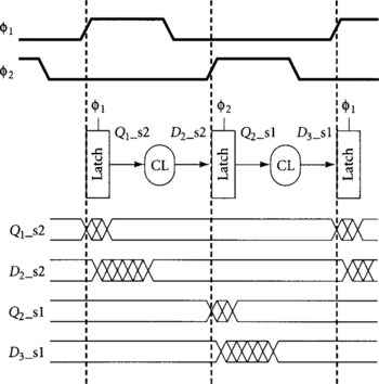
where T is the timing type, P is the phase, M is the monotonicity (if applicable), and Pol is the polarity (if applicable). For example, a sample path following these conventions is shown in Figure 4.13.
In addition to checking for correct timing and phase, we use timing types to verify monotonicity for domino gates.
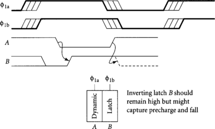
Note that, unlike Figure 4.11, we now use the same clock for precharge and evaluation of dynamic gates. Therefore, the definition of a valid signal changes: a valid signal settles before the falling edge of the clock and does not change until shortly after the falling edge of the clock. This is exactly the same timing rule as a qualified clock, so _v and _q signals are now in principle interchangeable. Nevertheless, we are much more concerned about controlling skew on clocks, so we reserve the _q timing type for clock signals and continue to use _v for dynamic outputs with the understanding that the length of the validity period is not as great as it was in a classical two-phase system. In particular, a _v1 signal is not a safe input to a φ1 static latch because the dynamic gate may precharge at the same time the latch samples. For example, Figure 4.14 illustrates how latch B’s output might incorrectly fall when dynamic gate A precharges if there is skew between the clocks of the two elements.
DEFINITION 2
The _v inputs to a dynamic gate must be monotonically rising (r). The output of a dynamic gate is monotonically falling (f).
This definition formalizes the requirement of monotonicity. _s inputs to a dynamic gate stabilize before the gate begins evaluation, so they do not have to be monotonic. As an example, a φ1 dynamic gate may take input X_v4r or Y_s1 or even Z_s1f but not W_v4f.
DEFINITION 3
Inverting static gates that accept exclusively monotonically rising inputs (r) produce monotonically falling outputs (f) and vice versa.
Guideline 2
Static gates should be skewed hi for monotonically falling (f) inputs and lo for monotonically rising (r) inputs.
Skewed gates may use different P/N ratios to favor the critical transitions and improve speed. hi-skew gates with large P/N ratios should follow monotonically falling dynamic outputs. When a path built with static logic is monotonic, alternating HI- and LO-skew gates can be used for speed. A normal inverter has a P/N ratio of about 2/1. A HI-skew inverter may have a P/N ratio of 4/1, while a LO-skew inverter has a P/N ratio of 1/1 to favor the critical transitions.
Guideline 3
_s and _v signals are the only legal data inputs to gates and latches. _q and φ are the only legal clock inputs.
This is identical to traditional two-phase conventions. Clocks and gates should not mix except at clock qualifiers (see Guideline 7).
GUIDELINE 4
The output timing type of a static gate is the intersection of the input types. If the intersection is empty, the gate is receiving an illegal set of inputs.
Remember that a _v signal can be sampled for a subset of the time that a _s signal of the same phase is stable. For example, a gate receiving _s12 and _v2 inputs produces a _v2 output. A gate receiving _s12 and _s34 inputs has no legal output timing type, so the inputs are incompatible.1
GUIDELINE 5
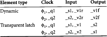
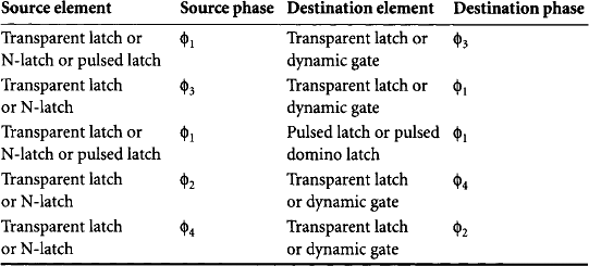
Table 4.2 summarizes timing rules for the most common elements in a system mixing skew-tolerant domino and transparent latches.
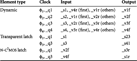
Clocked elements set the output timing type and require inputs which are valid when they may be sampled. The types depend on the clock phase used by the clocked element. See Table 4.3 (Guideline 6) for a complete list of timing rules covering more special cases.
The output of a dynamic gate is valid and monotonically falling during the phase the gate operates, just as we have seen for two-phase systems. The input can come from static or domino logic. Static inputs must be stable _s while the gate is in evaluation to avoid glitches. Inputs from domino logic are monotonic rising and thus only must be valid _v. The key difference between conventional timing types and skew-tolerant timing types is that valid inputs to the first dynamic gate in each phase come from the previous phase, while inputs to later dynamic gates come from the current phase. Technically, different series stacks may receive _v inputs from different phases.
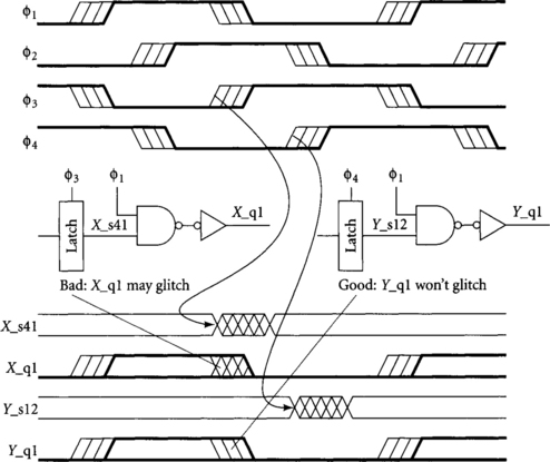
N-latches are used at the interface of domino to static logic. Although transparent latches could also be used, they are slower and present more clock load, so they are not recommended in this methodology. Notice that N-latches use a clock from one phase earlier than the dynamic gate they are latching to avoid race conditions by which that dynamic gate may precharge before the latch becomes opaque. Because of the single PMOS pullup in the N-latch, dynamic gate output A evaluating late can borrow time through the N-latch even after the latch clock falls, as shown in Figure 4.15.
The N-latch output B settles after the rising clock edge evaluating the preceding dynamic gate and remains stable until the next rising edge of the latch clock, so it is stable for one phase (Phase 3, in this example). Because the interface between dynamic and static logic normally occurs at half-cycle boundaries, the φ2 and φ4 N-latches are rarely used.
The output of a transparent latch stabilizes after the latch becomes transparent and remains stable until the latch becomes transparent again; for example, the output of a φ1 transparent latch is _s23. Signals stable for multiple phases are legal as inputs to elements requiring stability in either phase. For example, a _s23 signal is a legal input to a φ3 transparent latch that requires _s3. While transparent latches technically can accept certain _v inputs as we saw with two-phase timing types, N-latches are preferred at this interface of domino to static so only the _s inputs are shown in the table for transparent latches.
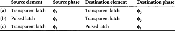
Figure 4.16 illustrates legal connections between static and domino gates. The top row of gates is a pipeline of static logic, while the bottom row is domino. Dynamic outputs must pass through N-C2MOS latches before driving static logic. Static signals can directly drive appropriate domino gates.
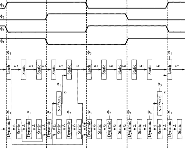
Figure 4.17 illustrates illegal connections between static and domino gates. Connection A is bad because the dynamic output will precharge while the φ3 latch is transparent, allowing incorrect data to propagate into the static logic. An N-latch should have been used at the interface. Connection B is bad because the static path skips over a latch. Connection C is bad because the φ4 domino gate receives both _v3 and _v4 inputs. By the time the _v4 input arrives, the _v3 result may have precharged. Each of these illegal connections violates the possible inputs of Table 4.2, so an automatic tool could flag these errors.

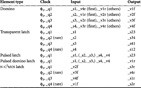
Now that we have seen how timing types work, we can expand them to handle pulsed latches and uncommon phases of latches. The complete guidelines are summarized in Table 4.3.
GUIDELINE 6
Inputs and outputs of clocked elements should match the timing types defined in Table 4.3.
φ2 and φ4 transparent latches are not normally used. They occasionally are useful, however, in short paths to avoid min-delay problems as we shall see in Section 4.1.6. φ2 and φ4 N-latches are also rare, but may be used to interface from the middle of a half-cycle of domino logic back to static logic. These rare latches have timing analogous to their more common counterparts.
Pulsed latches are controlled by a brief pulse derived from the rising edge of φ1· They accept any signal that will not change on or immediately after this edge (i.e., _s1, _s4, and _v4). The output has the same stable time as the output of a φ1 transparent latch because it stabilizes after the rising edge of φ1 and does not change until after the next rising edge of φ1· Unfortunately, we see that the output of a pulsed latch is _s23, but neither _s2 nor _s3 signals are safe inputs to pulsed latches, so it is unsafe for one pulsed latch to drive another. This matches our understanding that pulsed latches cannot be cascaded directly without logic between them because of hold time problems. In order to build systems with pulsed latches, we relax the timing rules to permit _s2 and _s3 inputs to pulsed latches, then check for min-delay on such inputs. Such checks are discussed further in Section 4.1.6.
Pulsed domino latches have the same input restrictions as pulsed latches, but produce a _v1r output suitable for domino logic because their outputs become valid after the rising edge of φ1 and remain valid until the falling edge of φ when the gate precharges.
4.1.5 Qualified Clocks
Qualified clocks are used to save power by disabling units or to build combination multiplexer-latches in which only one of several parallel latches is activated each cycle. Qualification must be done properly to avoid glitches.
GUIDELINE 7
Qualified clocks are produced by ANDing φi with a _s(i) signal in the clock buffer.
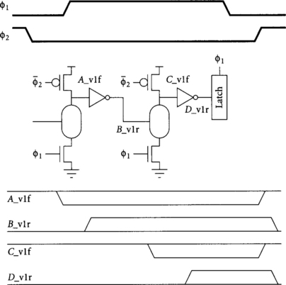
To avoid problems with clock skew, it is best to qualify the clock with a signal that will remain stable long after the falling edge of the clock. For example, Figure 4.18 shows two ways to generate a _q1 clock. The _s qualification signal must set up before φ1 rises and should not change until after φ1 falls. In the left circuit, we AND φ1 with a _s41 signal. If there is clock skew, the _s41 signal may change before φ1 falls, allowing the _q1 clock to glitch. Glitching clocks are very bad, so the right circuit, in which we AND φ1 with a _s12 signal, is much preferred. This problem is analogous to min-delay. Like min-delay, it could also be solved by delaying the _s41 signal so that it would not arrive at the AND gate before the falling edge of φ1· However, clock qualification signals are often critical, so it is unwise to delay them unnecessarily. The race could also be solved by making the skew between the φ1 and φ3 clocks in the left circuit small.
4.1.6 Min-Delay Checks
We have noted that two-phase systems usually use complementary clocks rather than nonoverlapping clocks and thus lose their strict safety properties, requiring explicit checks for min-delay violations. Similarly, the four-phase timing types of Section 4.1.4 use nonoverlapping and φ3 to achieve safety, but real systems typically would use 50% duty cycle clocks.
In this section, we describe where min-delay risks arise with 50% duty cycle clocks. We also examine the min-delay problems caused by pulsed latches.
Min-delay is a serious problem because unlike setup time violations, hold time violations cannot be fixed by adjusting the clock frequency. Instead, the designer must conservatively guarantee adequate delay through logic between clocked elements. Min-delay problems should be checked at the interfaces listed in Table 4.4. The top half of the table lists common cases encountered in typical designs. The bottom half of the table lists combinations, which while technically legal according to Table 4.2, would not occur in normal use because φ2 and φ4 transparent latches and N-latches are seldom used.
Min-delay problems can be solved in two ways. One approach is to add explicit delay to the data. For example, a buffer made from two long-channel inverters is a popular delay element. Another is to add a latch between the elements controlled by an intervening phase. Both approaches prevent races by slowing the data until the hold time of the second element is satisfied. Examples of these solutions are shown in Figure 4.19. In path (a) there is no logic between latches. If φ1 and φ3 are skewed as shown, data may depart the φ1 latch when it becomes transparent, then race through the φ3 latch before it becomes opaque. Path (b) solves this problem by adding logic delay δlogic, as was discussed in Section 2.2.4. Path (c) solves the problem by adding a φ2 latch. If the minimum required delay is large, the latch may occupy less area than a string of delay elements.
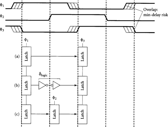
Figure 4.19 Solution to min-delay problem between φ1 and φ3 transparent latches: min-delay risk (a), extra gates (b), and extra latch (c)
Min-delay problems can actually occur at any interface, not just those listed in Table 4.4. For example, if clock skew were greater than a quarter cycle, min-delay problems could occur between φ1 and φ2 transparent latches. Because it is very difficult to design systems when the clock skew exceeds a quarter cycle, we will avoid such problems by requiring that the clock have less than a quarter cycle of skew between communicating elements.
Depending on the clock generation method, a few other connections may incur races. It is possible to construct clock generators with adjustable delays so that as the frequency reduces, the delay between each phase remains Tc/N. However, as we will see in Section 5.2.1, it may be more convenient to produce φ2 and φ4 by delaying φ1 and φ3, respectively, by a fixed amount. Such clock generators introduce the possibility of races that are frequency independent because the delay between phases is fixed.
One such risky connection is a φ1 pulsed latch feeding a φ2 domino gate. There is a max-delay condition that data must set up at the input of the domino gate before the gate enters evaluation. Clock skew between φ1 and φ2 reduces the nominally available quarter cycle. Since the delay from φ1 to φ2 is constant, if domino input does not set up in time, the circuit will fail at any clock frequency. The same problem occurs at the interface of a φ1 transparent latch to φ2 domino and of a φ3 transparent latch to φ4 domino.
Another min-delay problem occurs between φ2 transparent latches and φ1 pulsed latches or pulsed domino latches. Again, if the delay between phases is independent of frequency, hold time violations cannot be fixed by adjusting the clock frequency.
4.2 Clocked Element Design
This section offers guidelines on the design of fast clocked elements. Remember that static CMOS logic uses either transparent latches or pulsed latches. Domino logic uses no latches at all, except at the interface back to static logic, where N-latches should be used. We postpone discussion of supporting scan in clocked elements until Section 4.3.
Critical paths should be entirely domino wherever possible because we must budget skew and latch propagation delay when making a transition from static back into domino logic; moreover, time borrowing is not possible through the interface. Because most functions are nonmonotonic, this frequently dictates using dual-rail domino. In certain cases, dual-rail domino costs too much area, routing, or power. For high-speed systems, going entirely static may be faster than mixing domino and static and paying the interface overhead. If the overhead is acceptable because skew is tightly controlled, try combining as much of the nonmonotonic logic into static gates at the end of the block, as discussed in Section 3.2.1.
4.2.1 Latch Design
The fastest latches are simply transmission gates. To avoid the noise problems described in Section 2.3, the gates should be preceded and followed by static CMOS gates. These gates may perform logic rather than merely being buffers, so the latch presents very little timing overhead. Pulsed latches can be produced by simply pulsing the transmission gate control.
GUIDELINE 8
Use a transmission gate as a latch receiving input from a static logic block. Use a full keeper on the output for static operation.
The transmission gate latch is very fast and compact and is used in the DEC Alpha 21164 methodology. The output is a dynamic node and must obey dynamic node noise rules. Therefore, it should drive a static gate not far from the output. A φ1 static latch is shown in Figure 4.20.
GUIDELINE 9
Use a static gate before and after each static latch.
This gate is conventionally an inverter, but may be changed to any other static gate. The static gate after the latch should have no more than two inputs to avoid charge-sharing problems when the channel is not conducting. There should be little routing between the input gate, transmission gate, and output gate to minimize power supply noise problems and coupling onto the dynamic node. For synthesized blocks, it may be best to create versions of the latches incorporating gates into the input and output as a single cell because synthesis tools have difficulty estimating the delay of an unbuffered transmission gate and because place-and-route tools may produce unpredictable routing.
GUIDELINE 10
Generally use only pulsed latches or φ1 and φ3 transparent latches.
We select two phases to be the primary static latch clocks to resemble traditional two-phase design. The φ2 and φ4 clocks would be confusing if generally used, so they are restricted to use to solve min-delay problems in short paths.
GUIDELINE 11
Use an N-C2MOS latch on the output of domino logic driving static gates as shown in Figure 4.7. Use a full keeper on the output for static operation.
Again, the output is a dynamic node and must obey dynamic node noise rules. The N-latch is selected because it is faster and smaller than a tristate latch and doesn’t have the charge-sharing problems seen if a domino gate drove a transmission gate latch.
GUIDELINE 12
The domino gate driving an N-latch should be located adjacent to the latch and should share the same clock wire and VDD as the latch.
The N-latch has very little noise margin for noise on the positive supply. This noise can be minimized by keeping the latch adjacent to the domino output, thereby preventing significant noise coupling or VDDdrop. The latch is also sensitive to clock skew because if it closed too late, it could capture the precharge edge of the domino gate. Therefore, the same clock wire should be used to minimize skew.
4.2.2 Domino Gate Design
The guidelines in this section cover keepers, charge-sharing noise, and unfooted domino gates.
GUIDELINE 13
All dynamic gates must include a keeper.
In Section 4.3 we will see that the clock is stopped low during test, so a keeper is necessary to fight leakage on φ3 and φ4 dynamic gates. It is also necessary on all gates to achieve reasonable noise immunity. Breaking this guideline requires extremely careful attention to dynamic gate input noise margins.
GUIDELINE 14
The first dynamic gate of Phase 3 must include a full keeper.
As discussed in Section 3.2.3, this is necessary to prevent the outputs of the first Phase 3 gates from floating when the clock is stopped low and the Phase 2 gates precharge. Note that because the first dynamic gate of Phase 1 does not include a full keeper, the clock should not be stopped high long enough for the output to be corrupted by subthreshold leakage. Of course, this guideline is an artifact of the methodology; an alternative methodology that stopped the clock high or allowed clock stopping both high and low would require the full keeper on Phase 1. In Section 4.3.2 we will see that the last dynamic gate of Phase 4 may also need a full keeper to support scan.
GUIDELINE 15
Use secondary precharge devices on internal nodes to control charge-sharing noise.
The exact number of secondary precharge devices required depends on the noise budget. A reasonable rule of thumb is to precharge every other internal node (starting from the top), plus any internal node with a large amount of diffusion, as discussed in Section 3.2.4.
GUIDELINE 16
The output of a dynamic gate must drive the gate, not source/drain input of the subsequent gate.
The result of a dynamic gate is stored on the capacitance of the output node, so this guideline prevents charge-sharing problems. An important implication is that dynamic gates cannot drive transmission gate multiplexer data inputs, although they could drive tristate-based multiplexers.
GUIDELINE 17
Use footed dynamic gates exclusively.
This guideline is in place to avoid excess power consumption, which may occur when the pulldown transistors are all on while the gate is still precharging. It may be waived on the first φ2 and φ4 gates of each cycle so long as the inputs of the gates come from φ1 or φ3 domino logic that does not produce a rising output until the φ2 or φ4 gates have entered evaluation. Aggressive designers may waive the guideline on other dynamic gates if power consumption is tolerable.
4.2.3 Special Structures
In a real system, skew-tolerant domino circuits must interface to special structures such as memories, register files, and programmable logic arrays (PLAs). Precharged structures like register files are indistinguishable in timing from ordinary domino gates. Indeed, standard six-transistor register cells can produce dual-rail outputs suitable for immediate consumption by dual-rail domino gates.
Certain very useful dynamic structures such as wide comparators and dynamic PLAs are inherently nonmonotonic and are conventionally built for high performance using self-timed clocks to signal completion. The problem is that these structures are most efficiently implemented with cascaded wide dynamic gates because the delay of a dynamic NOR structure is only a weak function of the number of inputs. Generally, dynamic gates cannot be directly cascaded. However, if the second dynamic gate waits to evaluate until the first gate has completed evaluation, the inputs to the second gate will be stable and the circuit will compute correctly. The challenge is creating a suitable delay between gates. If the delay is too long, time is wasted. If the delay is too short, the second gate may obtain the wrong result.
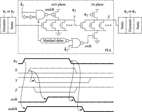
A common solution is to locally create a self-timed clock by sensing the completion of a model of the first dynamic gate. For example, Figure 4.21 shows a dynamic NOR-NOR PLA integrated into a skew-tolerant pipeline. The AND plane is illustrated evaluating during φ2, and adjacent logic can evaluate in the same or nearby phases. andclk is nominally in phase with φ2, but has a delayed falling edge to avoid a precharge race with the OR plane. The latest input X to the AND plane is used by a dummy row to produce a self-timed clock orclk for the OR plane that rises after AND plane output Yhas settled. Notice how the falling edge of orclk is not delayed so that when Y precharges high the OR plane will not be corrupted. The output Z of the OR plane is then indistinguishable from any other dynamic output and can be used in subsequent skew-tolerant domino logic.
4.3 Testability
As integrated circuits use ever more transistors and overlay the transistors with an increasing number of metal layers, debug and functional test become more difficult. Packaging advances such as flip-chip technology make physical access to circuit nodes harder. Hence, engineers employ design for testability methods, trading area and even some amount of performance to facilitate test. The most important testability technique is scan, in which memory elements are made externally observable and controllable through a scan chain [66]. Scan generally involves modifying flip-flops or latches to add scan signals.
Because scan provides no direct value to most customers, it should impact a design as little as possible. A good scan technique has
The area criterion implies that scan should add little extra cell area and also few extra wires. The timing-critical scan signal criterion is important because scan should not introduce critical paths or require analysis and timing verification of the scan logic. Clock gating is costly because it increases clock skew and may increase the setup on already critical clock enable signals such as global stall requests.
We will assume that scan is performed by stopping the global clock low (i.e., φ1 and φ2 low and φ3 and φ4 high), then toggling scan control signals to read out the current contents of memory elements and write in new contents. We will first review scan of transparent and pulsed latches, then extend the method to scan skew-tolerant domino gates in a very similar fashion.
4.3.1 Static Logic
Systems built from transparent latches or pulsed latches can be made observable and controllable by adding scan circuitry to every cycle of logic. Figure 4.22 shows a scannable latch. Normal latch operation involves input D, output Q, and clock φ. When the clock is stopped low, the latch is opaque. The circuits shown in the dashed boxes are added to the basic latch for scan. The contents of latch can be scanned out to SDO (scan data out) and loaded from SDI (scan data in) by toggling the scan clocks SCA and SCB. While it is possible to use a single scan clock, the two-phase nonoverlapping scan clocks shown are more robust and simplify clock routing. The small inverters represent weak feedback devices; they must be ratioed to allow proper writing of the cell. Note that this means the gate driving the data input D must be strong enough to overpower the feedback inverter. Although a tristate feedback gate may be used instead, it must still be weak enough to be overpowered by SDI during scan.
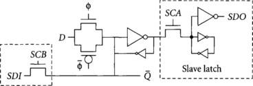
We assume that scan takes place while the clock is stopped low. Therefore, transparent latch systems make the first half-cycle latch scannable, and pulsed latch systems make the pulsed latch scannable. The procedure for scan is
4.3.2 Domino Logic
Because skew-tolerant domino does not use latches, some other method must be used to observe and control one node in each cycle. Controlling a node requires cutting off the normal driver of the node and activating an access transistor. For example, latches are controlled during scan by being made opaque, then activating the SCB access transistor in Figure 4.22. A dynamic gate with a full keeper can be controlled in an analogous way by turning off both the evaluation and precharge transistors and turning on an access transistor, as shown in Figure 4.23. Notice that separate evaluation and precharge signals are necessary to turn off both devices so a gated clock φs is introduced. A slave latch connected to the full keeper provides observability without loading the critical path, just as it does on a static latch. Note that this is a ratioed circuit and the usual care must be taken that feedback inverters are sufficiently weak in all process corners to be overpowered. Also, note that only a PMOS keeper is required on the dynamic output node if SCA and SCB are toggled quickly enough that leakage is not a problem.
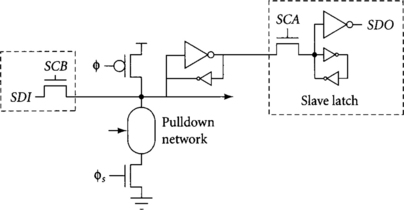
Which dynamic gate in a cycle should be scannable? The gate should be chosen so that during scan, the subsequent domino gate is precharging so that glitches will not contaminate later circuits. The gate should also be chosen so that when normal operation resumes, the output will hold the value loaded by scan until it is consumed.
Let us assume that scan is done while the global clock is stopped low, thus with the φ1 and φ2 domino gates in the first half-cycle precharging and the φ3 and φ4 gates in the second half-cycle evaluating. Then a convenient choice is to scan the last φ4 domino gate in the cycle. This means that the last φ4 domino gate must include a full keeper. Scan is done with the following procedure:
When gclk is stopped, the scannable gate will have evaluated to produce a result. Stopping φs low will turn off the evaluation transistor to the scannable gate, leaving the output on the dynamic node held only by the full keeper. Toggling SCA and SCB will advance the result down the scan chain and load a new value into the dynamic gate. When gclk restarts, it rises, allowing the gates in the first half-cycle to evaluate with the data stored on the scan node. Once the scannable gate begins precharging, φs can be released because the gate no longer needs to be cut off from its inputs.
Unfortunately, this scheme requires releasing φs in a fraction of a clock cycle. It would be undesirable to do this with a global control signal because it is difficult to get a global signal to all parts of the chip in a tightly controlled amount of time. It is better to use a small amount of logic in the local clock generator to automatically perform Steps 2 and 5. We will examine such a clock generator supporting four-phase skew-tolerant domino with clock enabling and scan in Section 5.2.3.
A potential difficulty with scanning dynamic gates is that it could double the size of a dynamic cell library if both scannable and normal dynamic gates are provided. A solution to this problem is to provide a special scan cell that “bolts on” to an ordinary dynamic gate. The scan cell adds a full keeper and scan circuitry to the ordinary gate’s pmos keeper, as shown in Figure 4.24. In ordinary usage, the two clock inputs of the dynamic gate are shorted to φ4, while in a scannable gate φ4 and φ4s are connected.
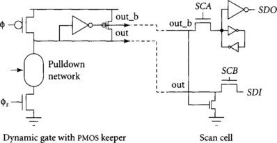
GUIDELINE 19
Make the last domino gate of each cycle scannable with bolt-on scan logic.
A cycle may combine static and domino logic. As long as all first half-cycle latches and the last domino gate in each second half-cycle are scanned, the cycle is fully testable. Static and domino scan nodes are compatible and may be mixed in the same scan chain. Note that pulsed domino latches are treated as first half-cycle domino gates and are not scanned.
4.4 Historical Perspective
Circuit methodologies are seldom published, although employee turnover in Silicon Valley tends to carry the best techniques from one company to another in a clandestine fashion. The best-documented methodologies have been from IBM and DEC. DEC (now Compaq) has led the pack in circuit performance since the introduction of the Alpha 21064, so we will follow the evolution of their circuit methodology. In the next historical perspective, we will follow the DEC clocking methodology.
The Alpha 21064 [16, 17] arrived in 1993 at a blazing 200 MHz while other microprocessors were running 40–100 MHz. This speed corresponds to approximately 20 fanout-of-4 inverter delays per cycle in the 0.75-micron process. Earlier DEC chips had used a four-phase nonoverlapping clock system distributed on multiple clock wires to avoid risk of min-delay. To achieve acceptable skew at 200 MHz, the Alpha used a single global clock wire. The processor used true single-phase clock (TSPC) transparent latches and avoided min-delay problems through clock distribution and latch design. Logic could be built into the first stage of the TSPC latches.
The Alpha 21164 [5, 6, 27] arrived two years later at 300 MHz, using fewer than 18 FO4 inverter delays per cycle in the 0.5-micron process [30]. The designers found that an ordinary transparent latch was faster than the TSPC latch [26], especially because logic could be integrated into both the gate before and after the latch. Min-delay was avoided by requiring at least one minimum logic delay element between all latches and was verified by a simple CAD tool. The 21164 was also the first published processor to eliminate a latch from the middle of a cycle of domino logic by overlapping clocks.
Curiously, the Alpha 21264 [28] broke away from the skew-tolerant techniques advocated in this book. It shipped at 575 MHz in late 1998 in a 0.35-micron process. The processor uses an unusual edge-triggered flip-flop [28] instead of transparent latches. This apparently sacrifices skew tolerance and increases the latching overhead as a fraction of cycle time, although it does provide a sense amplifier for special low-swing differential signals. Min-delay risks are increased due to the more complex clocking scheme and are avoided by careful checking with a CAD tool.
4.5 Summary
This chapter has described a method for designing systems with transparent and pulsed latches and skew-tolerant domino. It uses a single globally distributed clock from which four local overlapping clock phases are derived. The methodology supports stopping the clock low for power savings and testability and describes a low-overhead scan technique compatible with both domino and static circuits. Timing types are used to verify proper connectivity among the clocked elements.
The methodology hides sequencing overhead everywhere except at the interface between static and domino logic. At the interface of domino-to-static logic, a latch is necessary to hold the result, adding propagation delay to the critical path. More importantly, at the interface of static-to-domino logic, clock skew must be budgeted so that inputs settle before the earliest the evaluation clock might rise, yet the domino gate may not begin evaluation until the latest time the clock might rise. This overhead makes it expensive to switch between static and domino logic. Designers who need domino logic to meet cycle time targets should therefore consider implementing their entire path in domino. Because single-rail domino cannot implement nonmonotonic functions, dual-rail domino is usually necessary. Therefore, we should expect to see more critical paths built entirely from dual-rail domino as sequencing overhead becomes a greater portion of the cycle time.
4.6 Exercises
[15] 4.1. Define time borrowing. Which of the following circuits permit time borrowing: transparent latches, pulsed latches, flip-flops, traditional domino circuits, skew-tolerant domino circuits?
[25] 4.2. Draw timing loop diagrams like those of Figure 4.4 for the path in Figure 4.25 assuming cycle times of 1.5, 1, and 0.8 units using the following combinational logic delays. Note which latches borrow time and if setup time violations occur.
[15] 4.3. Label the timing types of each connection in the circuit in Figure 4.25 using the two-phase timing types defined in this chapter. Assume the flop is built from two back-to-back transparent latches, the first controlled by clk_b and the second controlled by clk.
[20] 4.4. Label the timing types of each connection in the circuit in Figure 4.26 using the two-phase timing types defined in this chapter.
Figure 4.26 Path for Exercise 4.4
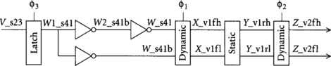
[20] 4.5. Label the timing types of each connection in the circuit in Figure 4.27 using the four-phase domino timing types defined in this chapter.
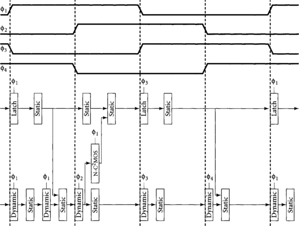
Figure 4.27 Path for Exercise 4.5
[40] 4.6. CAD project: Construct a time_check tool. The tool should accept a netlist of four types of elements: S (static), D (dynamic), L (transparent latch), and N (n-C2mos latch). Each element has an output and one or more inputs. Nonstatic elements also have a clock input. The tool should identify the timing type of each net and report elements with illegal input timing types.
[15] 4.7. Determine the minimum delay δlogic between the circuits in Table 4.5 in terms of δCQ, δCD, tskew, and the pulsed latch pulse width tpw.
1This guideline has an obscure exception. A static gate may receive both _s2 and _v1f inputs. Its output is a special type (let us say _vlrs2) only suitable as an input to a φ2 dynamic gate. This would occur when an inverting static gate receives inputs from a φ1 static latch and a φ1 dynamic gate in order to drive a φ2 dynamic gate. Similar combinations are legal inputs to other phases of domino gates.