
Introduction
Most digital systems today are constructed using static CMOS logic and edge-triggered flip-flops. Although such techniques have been adequate in the past and will remain adequate in the future for low-performance designs, they will become increasingly inefficient for high-performance components as the number of gates per cycle dwindles and clock skew becomes a greater problem. Designers will therefore need to adopt circuit techniques that can tolerate reasonable amounts of clock skew without an impact on the cycle time. Transparent latches offer a simple solution to the clock skew problem in static CMOS logic. Unfortunately, static CMOS logic is inadequate to meet timing objectives of the highest-performance systems. Therefore, designers turn to domino circuits, which offer greater speed. Unfortunately, traditional domino clocking methodologies [92] lead to circuits that have even greater sensitivity to clock skew and thus can defeat the raw speed advantage of the domino gates. Expert designers of microprocessors and other high-performance systems have long recognized the costs of edge-triggered flip-flops and traditional domino circuits and have used transparent latches and developed a variety of mostly proprietary domino clocking approaches to reduce the overhead. This book formalizes and analyzes skew-tolerant domino circuits, a method of controlling domino gates with multiple overlapping clock phases. Skew-tolerant domino circuits eliminate clock skew from the critical path, hiding the overhead and offering significant performance improvement.
In this chapter, we begin by examining conventional systems built from flip-flops. We see how these systems have overhead that eats into the time available for useful computation. We then examine the trends in throughput and latency for high-performance systems and see that, although the overhead has been modest in the past, flip-flop overhead now consumes a large and increasing portion of the cycle. We turn to transparent latches and show that they can tolerate reasonable amounts of clock skew, reducing the overhead. Next, we examine domino circuits and look at traditional clocking techniques. These techniques have overhead even more severe than that paid by flip-flops. However, by using overlapping clocks and eliminating latches, we find that skew-tolerant domino circuits eliminate all of the overhead. Three case studies illustrate the need for skew-tolerant circuit design.
In Chapter 2, we take a closer look at static CMOS latching techniques, comparing the design and timing of flip-flops, transparent latches, and pulsed latches. We discuss min-delay constraints necessary for correct operation and time borrowing that can help balance logic when used properly. There have been a host of proposed latch designs; we evaluate many of the designs and conclude that the common, simple designs are usually best. For high-performance systems, static CMOS circuits are often too slow, so domino gates are employed. In Chapter 3, we look at skew-tolerant domino design and timing issues. A practical methodology must efficiently combine both static and domino components, so Chapter 4 discusses methodology issues including the static/domino interface, testability, and timing types for high-level verification of proper connectivity. Because we are discussing skew-tolerant circuit design, we are very concerned about the clock waveforms. Chapter 5 explores methods of generating and distributing clocks suitable for skew-tolerant circuits, examines the sources of clock skew in these methods, and describes ways to minimize this skew. Conventional timing analysis tools either cannot handle clock skew or budget it in conservative ways. Chapter 6 describes the problem of timing analysis in skew-tolerant systems and presents simple algorithms for analysis. Finally, Chapter 7 concludes the book by summarizing the main results and greatest future challenges.
1.1 Overhead in Flip-Flop Systems
Most digital systems designed today use positive edge-triggered flip-flops as the basic memory element. A positive edge-triggered flip-flop is often referred to simply as an edge-triggered flip-flop, a D flip-flop, a master-slave flip-flop, or colloquially, just a flop. It has three terminals: input D, clock φ, and output Q. When the clock makes a low-to-high transition, the input D is copied to the output Q. The clock-to-Q delay, ΔCQ, is the delay from the rising edge of the clock until the output Q becomes valid. The setup time, ΔDC, is how long the data input D must settle before the clock rises for the correct value to be captured.
Figure 1.1 illustrates part of a static CMOS system using flip-flops. The logic is drawn underneath the clock corresponding to when it operates. Flip-flops straddle the clock edge because input data must set up before the edge and the output becomes valid sometime after the edge. The heavy dashed line at the clock edge represents the cycle boundary. After the flip-flop, data propagates through combinational logic built from static CMOS gates. Finally, the result is captured by a second flip-flop for use in the next cycle.
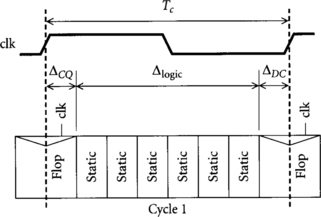
How much time is available for useful work in the combinational logic, Δlogic? If the cycle time is Tc, we see that the time available for logic is the cycle time minus the clock-to-Q delay and setup time:
Unfortunately, real systems have imperfect clocks. On account of mismatches in the clock distribution network and other factors that we will examine closely in Chapter 5, the clocks will arrive at different elements at different times. This uncertainty is called clock skew and is represented in Figure 1.2 by a hash of width tskew, indicating a range of possible clock transition times. The bold clock lines indicate the latest possible clocks, which define worst-case timing. Data must set up before the earliest the clock might arrive, yet we cannot guarantee data will be valid until the clock-to-Q delay after the latest clock.
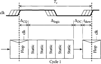
Now we see that the clock skew appears as overhead, reducing the amount of time available for useful work:
Flip-flops suffer from yet another form of overhead: imbalanced logic. In an ideal machine, logic would be divided into multiple cycles in such a way that each cycle had exactly the same logic delay. In a real machine, the logic delay is not precisely known at the time cycles are partitioned, so some cycles have more logic and some have less logic. The clock frequency must be long enough for the longest cycles to work correctly, meaning excess time in shorter cycles is wasted. The cost of imbalanced logic is difficult to quantify and can be minimized by careful design, but is nevertheless important.
In summary, systems constructed from flip-flops have overhead of the flip-flop delay (ΔDC and ΔCQ), clock skew (tskew), and some amount of imbalanced logic. We will call this total penalty the sequencing overhead.1 In the next section, we will examine trends in system objectives that show sequencing overhead makes up an increasing portion of each cycle.
1.2 Throughput and Latency Trends
Designers judge their circuit performance by two metrics: throughput and latency. Throughput is the rate at which data can pass through a circuit; it is related to the clock frequency of the system, so we often discuss cycle time instead. Latency is the amount of time for a computation to finish. Simple systems complete the entire computation in one cycle, so latency and throughput are inversely related. Pipelined systems break the computation into multiple cycles called pipeline stages. Because each cycle is shorter, new data can be fed to the system more often and the throughput increases. However, because each cycle has some sequencing overhead from flip-flops or other memory elements, the latency of the overall computation gets longer. For many applications, throughput is the most important metric. However, when one computation is dependent on the result of the previous, the latency of the previous computation may limit throughput because the system must wait until the computation is done. In this section, we will review the relationships among throughput, latency, computation length, cycle time, and overhead. We will then look at the trends in cycle time and find that the impact of overhead is becoming more severe.
When measuring delays, it is often beneficial to use a process-independent unit of delay so that intuition about delay can be carried from one process to another. For example, if I am told that the Hewlett-Packard PA8000 64-bit adder has a delay of 840 ps, I have difficulty guessing how fast an adder of similar architecture would work in my process. However, if I am told that the adder delay is seven times the delay of a fanout-of-4 (FO4) inverter, where an FO4 inverter is an inverter driving four identical copies, I can easily estimate how fast the adder will operate in my process by measuring the delay of an FO4 inverter. Similarly, if I know that microprocessor A runs at 50 MHz in a 1.0-micron process and that microprocessor B runs at 200 MHz in a 0.6-micron process, it is not immediately obvious whether the circuit design of B is more or less aggressive than A. However, if I know that the cycle time of microprocessor A is 40 FO4 inverter delays in its process and that the cycle time of microprocessor B is 25 FO4 inverter delays in its process, I immediately see that B has significantly fewer gate delays per cycle and thus required more careful engineering. The fanout-of-4 inverter is particularly well suited to expressing delays because it is easy to determine, because many designers have a good idea of the FO4 delay of their process, and because the theory of logical effort [82] predicts that cascaded inverters drive a large load fastest when each inverter has a fanout of about 4.
1.2.1 Impact of Overhead on Throughput and Latency
Suppose a computation involves a total combinational logic delay X. If the computation is pipelined into N stages, each stage has a logic delay Δlogic = X/N. As we have seen in the previous section, the cycle time is the sum of the logic delay and the sequencing overhead:
The latency of the computation is the sum of the logic delay and the total overhead of all N stages:
Equations 1.3 and 1.4 show how the impact of a fixed overhead increases as a computation is pipelined into more stages of shorter length. The overhead becomes a greater portion of the cycle time Tc, so less of the cycle is used for useful computation. Moreover, the latency of the computation actually increases with the number of pipe stages N because of the overhead. Because latency matters for some computations, system performance can actually decrease as the number of pipe stages increases.
EXAMPLE 1.1
Consider a system built from static CMOS logic and flip-flops. Let the setup (ΔDC) and clock-to-Q (ΔCQ) delays of the flip-flop be 1.5 FO4 inverter delays. Suppose the clock skew (tskew) is 2 FO4 inverter delays. What percentage of the cycle is wasted by sequencing overhead if the cycle time Tc is 40 FO4 delays? 24 FO4 delays? 16 TFO4 delays? 12 FO4 delays?
SOLUTION
The sequencing overhead is 1.5 + 1.5 + 2 = 5 FO4 delays. The percentage of the cycle consumed by overhead is shown in Table 1.1. This example shows that although the sequencing overhead was small as a percentage of cycle time when cycles were long, it becomes very severe as cycle times shrink.
The exponential increase in microprocessor performance, doubling about every 18 months [36], has been caused by two factors: better microarchitectures that increase the average number of instructions executed per cycle (IPC), and shorter cycle times. The cycle time improvement is a combination of steadily improving transistor performance and better circuit design using fewer gate delays per cycle. To evaluate the importance of sequencing overhead, we must tease apart these elements of performance increase to identify the trends in gates per cycle. Let us look both at the historical trends of Intel microprocessors and at industry predictions for the future.
1.2.2 Historical Trends
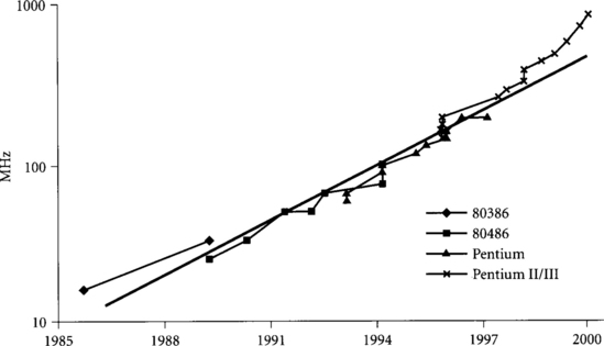
Figure 1.3 shows a plot of Intel microprocessor performance from the 16 MHz 80386 introduced in 1985 to the 800 MHz Pentium II processors selling in 1999 [42, 57]. The performance has increased at an incredible 53% per year, thus doubling every 19.5 months. This exponential increase in processor performance is often called “Moore’s law” [59], although technically Gordon Moore’s original predictions only referred to the exponential growth of transistors per integrated circuit, not the performance growth.
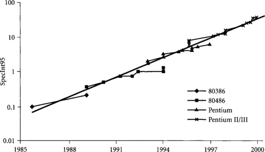
Figure 1.3 Intel microprocessor performance
Note: Performance is measured in SpecInt95. For processors before the 90 MHz Pentium, SpecInt95 is estimated from published MIPS data with the conversion 1 MIPS = 0.0185 SpecInt95.
Figure 1.4 shows a plot of the processor clock frequencies, increasing at a rate of 30% per year. Some of this increase comes from faster transistors, and some comes from using fewer gates per cycle.
Because we are particularly interested in the number of FO4 inverters per cycle, we need to estimate how FO4 delay improves as transistors shrink. Figure 1.5 shows the FO4 inverter delay of various MOSIS processes over many years. The delays are linearly scaling with the feature size and, averaging across voltages commonly used at each feature size, are well fit by the equation
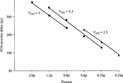
where f is the minimum drawn channel length measured in microns and delay is measured in picoseconds.
Using this delay model and data about the process used in each part, we can determine the number of FO4 delays in each cycle, shown in Figure 1.6. Notice that for a particular product, the number of gate delays in a cycle is initially high and gradually decreases as engineers tune critical paths in subsequent revisions on the same process and jumps as the chip is compacted to a new process that requires retuning. Overall, the number of FO4 delays per cycle has decreased at 12% per year.
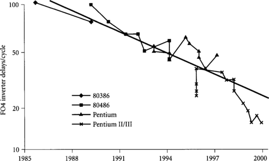
Putting everything together, we find that the 1.53 times annual historical performance increase can be attributed to 1.17 times from microarchitectural improvements, 1.17 times from process improvements, and 1.12 times from fewer gate delays per cycle.
1.2.3 Future Predictions
The Semiconductor Industry Association (SIA) issued a roadmap in 1997 [71] predicting the evolution of semiconductor technology over the next 15 years. Although such predictions are always fraught with peril, let us look at what the predictions imply for cycle times in the future.
Table 1.2 lists the year of introduction and estimated local clock frequencies predicted by the SIA for high-end microprocessors in various processes. The SIA assumes that future chips may have very fast local clocks serving small regions, but will use slower clocks when communicating across the die. The table also contains the predicted FO4 delays per cycle using a formula that
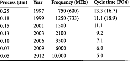
which better matches the delay of 0.25- and 0.18-micron processes than does Equation 1.5; these current processes are a more appropriate operating point to linearize around when predicting the future. The predictions proved somewhat optimistic in 1997 and 1999.
This roadmap shows a 7% annual reduction in cycle time. The predicted cycle time of only 5 FO4 inverter delays in a 0.05-micron process seems at the very shortest end of feasibility because it is nearly impossible for a loaded clock to swing rail to rail in such a short time. Nevertheless, it is clear that sequencing overhead of flip-flops will become an unacceptable portion of the cycle time.
1.2.4 Conclusions
In summary, we have seen that sequencing overhead was negligible in the 1980s when cycle times were nearly 100 FO4 delays. As cycle times measured in gate delays continue to shrink, the overhead becomes more important and is now a major and growing obstacle for the design of high-performance systems. We have not discussed clock skew in this section, but we will see in Chapter 5 that clock skew, as measured in gate delays, is likely to grow in future processes, making that component of overhead even worse. Clearly, flip-flops are becoming unacceptable, and we need to use better design methods that tolerate clock skew without introducing overhead. In the next section, we will see how transparent latches accomplish exactly that.
1.3 Skew-Tolerant Static Circuits
We can avoid the clock skew penalties of flip-flops by instead building systems from two-phase transparent latches, as has been done since the early days of CMOS [56]. Transparent latches have the same terminals as flip-flops: data input D, clock φ, and data output Q. When the clock is high, the latch is transparent and the data at the input D propagates through to the output Q. When the clock is low, the latch is opaque and the output retains the value it last had when transparent. Transparent latches have three important delays. The clock-to-Q delay, ΔCQ, is the time from when the clock rises until data reaches the output. The D-to-Q delay, ΔDQ, is the time from when new data arrives at the input while the latch is transparent until the data reaches the output. ΔCQ is typically somewhat longer than ΔDQ. The setup time, ΔDC, is how long the data input D must settle before the clock falls for the correct value to be captured.
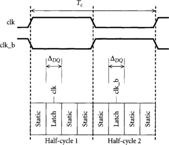
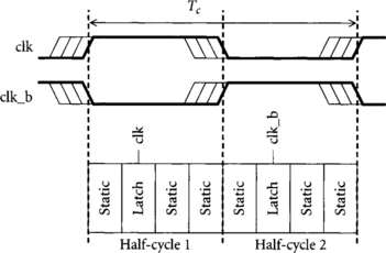
Figure 1.7 illustrates part of a static CMOS system using a pair of transparent latches in each cycle. One latch is controlled by clk, while the other is controlled by its complement clk_b. In this example, we show the data arriving at each latch midway through its half-cycle. Therefore, each latch is transparent when its input arrives and incurs only a D-to-Q delay rather than a clock-to-Q delay. Because data arrives well before the falling edge of the clock, setup times are trivially satisfied.
How much time is available for useful work in the combinational logic, Δlogic? If the cycle time is Tc, we see that
We will see in Chapter 2 that flip-flops are built from pairs of back-to-back latches so that the time available for logic in systems with no skew is about the same for flip-flops and transparent latches. However, transparent-latch systems can tolerate clock skew without cycle time penalty, as seen in Figure 1.8. Although the clock waveforms have some uncertainty from skew, the clock is certain to be high when data arrives at the latch so the data can propagate through the latch with no extra overhead. Data still arrives well before the earliest possible skewed clock edge, so setup times are still satisfied.
Finally, static latches avoid the problem of imbalanced logic through a phenomenon called time borrowing, also known as cycle stealing by engineers at Big Blue. We see from Figure 1.8 that each latch can be placed in any of a wide range of locations in its half-cycle and still be transparent when the data arrives. This means that not all half-cycles need to have the same amount of static logic. Some can have more and some can have less, meaning that data arrives at the latch later or earlier without wasting time as long as the latch is transparent at the arrival time. Hence, if the pipeline is not perfectly balanced, a longer cycle may borrow time from a shorter cycle so that the required clock period is the average of the two rather than the longer value. In Chapter 2 we will quantify how much time borrowing is possible.
In summary, systems constructed from transparent latches still have overhead from the latch propagation delay (ΔDQ) but eliminate the overhead from reasonable amounts of clock skew and imbalanced logic. This improvement is especially important as cycle times decrease, justifying a switch to transparent latches for high-performance systems.
1.4 Domino Circuits
To construct systems with fewer gate delays per cycle, designers may invent more efficient ways to implement particular functions or may use faster gates. The increasing transistor budgets allow parallel structures that are faster; for example, adders progressed from compact but slow ripple carry architectures to larger carry look-ahead designs to very fast but complex tree structures. However, there is a limit to the benefits from using more transistors, so designers are increasingly interested in faster circuit families, in particular domino circuits. Domino circuits are constructed from alternating dynamic and static gates. In this section, we will examine how domino gates work and see why they are faster than static gates. Gates do not exist in a vacuum; they must be organized into pipeline stages. When domino circuits are pipelined in the same way that two-phase static circuits have traditionally been pipelined, they incur a great deal of sequencing overhead from latch delay, clock skew, and imbalanced logic. By using overlapping clocks and eliminating the latches, we will see that skew-tolerant domino circuits can hide this overhead to achieve dramatic speedups.
1.4.1 Domino Gate Operation
To understand the benefits of domino gates, we will begin by analyzing the delay of a gate. Remember that the time to charge a capacitor is
For now we will just consider gates that swing rail to rail, so ΔV is VDD. If a gate drives an identical gate, the load capacitance and input capacitance are equal (neglecting parasitics), so it is reasonable to consider the C/I ratio of the gate’s input capacitance to the current delivered by the gate as a metric of the gate’s speed. This ratio is called the logical effort [82] of the gate and is normalized to one for a static CMOS inverter. It is higher for more complex static CMOS gates because series transistors in complex gates must be larger and thus have more input capacitance to deliver the same output current as an inverter.
Static circuits are slow because inputs must drive both NMOS and PMOS transistors. Only one of the two transistors is on, meaning that the capacitance of the other transistor loads the input without increasing the current drive of the gate. Moreover, the PMOS transistor must be particularly large because of its poor carrier mobility and thus adds much capacitance.
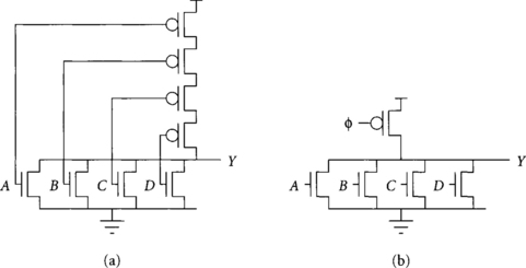
A dynamic gate replaces the large, slow PMOS transistors of a static CMOS gate with a single clocked PMOS transistor that does not load the input. Figure 1.9 compares static and dynamic NOR gates. The dynamic gates operate in two phases: precharge and evaluation. During the precharge phase, the clock is low, turning on the PMOS device and pulling the output high. During the evaluation phase, the clock is high, turning off the PMOS device. The output of the gate may evaluate low through the NMOS transistor stack.
The dynamic gate is faster than the static gate for two reasons. One is the greatly reduced input capacitance. Another is the fact that the dynamic gate output begins switching when the input reaches the transistor threshold voltage, Vt. This is sooner than the static gate output, which begins switching when the input passes roughly VDD/2. This improved speed comes at a cost, however: dynamic gates must obey precharge and monotonicity rules, are more sensitive to noise, and dissipate more power because of their higher activity factors.
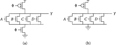
The precharge rule says that there must be no active path from the output to ground of a dynamic gate during precharge. If this rule is violated, there will be contention between the PMOS precharge transistor and the NMOS transistors pulling to ground, consuming excess power and leaving the output at an indeterminate value. Sometimes the precharge rule can be satisfied by guaranteeing that some inputs are low. For example, in the four-input NOR gate, all four inputs must be low during precharge. In a four-input NAND gate, if any input is low during precharge, there will be no contention. It is commonly not possible to guarantee inputs are low, so often an extra clocked evaluation transistor is placed at the bottom of the dynamic pulldown stack, as shown in Figure 1.10. Gates with and without clocked evaluation transistors are sometimes called footed and unfooted [62]. Unfooted gates are faster but require more complex clocking to prevent both PMOS and NMOS paths from being simultaneously active.
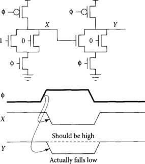
The monotonicity rule states that all inputs to dynamic gates must make only low-to-high transitions during evaluation. Figure 1.11 shows a circuit that violates the monotonicity rule and obtains incorrect results. The circuit consists of two cascaded dynamic NOR gates. The first computes X = NOR(1, 0) = 0. The second computes Y = NOR(X, 0), which should be 1. Node X is initially high and falls as the first nor gate evaluates. Unfortunately, the second nor gate sees that input X is high when φ rises and thus pulls down output Y incorrectly. Because the dynamic nor gate has no pmos transistors connected to the input, it cannot pull Y back high when the correct value of X arrives, so the circuit produces an incorrect result. The problem occurred because X violated the monotonicity rule by making a high-to-low transition while the second gate is in evaluation.
It is not possible to cascade dynamic gates directly with the same clock without violating the monotonicity rule because each dynamic output makes a high-to-low transition during evaluation while dynamic inputs require low-to-high transitions during evaluation. An easy way to solve the problem is to insert an inverting static gate between dynamic gates, as shown in Figure 1.12. The dynamic/static gate pair is called a domino gate, which is slightly misleading because it is actually two gates. A cascade of domino gates precharge simultaneously like dominos being set up. During evaluation, the first dynamic gate falls, causing the static gate to rise, the next dynamic gate to fall, and so on like a chain of dominos toppling.
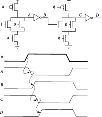
Unfortunately, to satisfy monotonicity we have constructed a pair of or gates rather than a pair of nor gates. In Chapter 3 we will return to the monotonicity issue and see how to implement arbitrary functions with domino gates.
Mixing static gates with dynamic gates sacrifices some of the raw speed offered by the dynamic gate. We can regain some of this performance by using HI-skew2 static gates with wider-than-usual PMOS transistors [82] to speed the critical rising output during evaluation. Moreover, the static gates may perform arbitrary functions rather than being just inverters [87]. All considered, domino logic runs 1.5 to 2 times faster than static CMOS logic [49] and is therefore attractive enough for high-speed designs to justify its extra complexity.
1.4.2 Traditional Domino Clocking
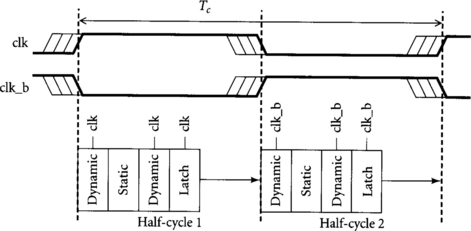
After domino gates evaluate, they must be precharged before they can be used in the next cycle. If all domino gates were to precharge simultaneously, the circuit would waste time while only precharging, not useful computation, takes place. Therefore, domino logic is conventionally divided into two phases or half-cycles, ping-ponged such that the first phase evaluates while the second precharges, and then the first phase precharges while the second evaluates. In a traditional domino clocking scheme [92], latches are used between phases to sample and hold the result before it is lost to precharge, as illustrated in Figure 1.13. The scheme appears very similar to the use of static logic and transparent latches discussed in the previous section. Unfortunately, we will see that such a scheme has enormous sequencing overhead.

With ideal clocks, the first dynamic gate begins evaluating as soon as the clock rises. Its result ripples through subsequent gates and must arrive at the latch a setup time before the clock falls. The result propagates through the latch, so the overhead of each latch is the maximum of its setup time and D-to-Q propagation delay. The latter time is generally larger, so the total time available for computation in the cycle is
Unfortunately, a real pipeline like that shown in Figure 1.14 experiences clock skew. In the worst case, the dynamic gate and latch may have greatly skewed clocks. Therefore, the dynamic gate may not begin evaluation until the latest skewed clock, while the latch must set up before the earliest skewed clock. Hence, clock skew must be subtracted not just from each cycle, as it was in the case of a flip-flop, but from each half-cycle! Assuming the sum of clock skew and setup time are greater than the latch D-to-Q delay, the time available for useful computation becomes
As with flip-flops, traditional domino pipelines also suffer from imbalanced logic. In summary, traditional domino circuits are slow because they pay overhead for latch delay, clock skew, and imbalanced logic. In the case study of the Alpha 21164 microprocessor in Section 1.5.2, we will see that this overhead can easily reach a quarter of the cycle time.
1.4.3 Skew-Tolerant Domino
Both flip-flops and traditional domino circuits launch data on one edge and sample it on another. These edges are called hard edges or synchronization points because the arrival of the clock determines the exact timing of data. Even if data is available early, the hard edges prevent subsequent stages from beginning early. Static CMOS pipelines with transparent latches avoided the hard edges and therefore could tolerate some clock skew and use time borrowing to compensate for imbalanced logic. Some domino designers have recognized that this fundamental idea of softening the hard clock edges can be applied to domino circuits as well. Although a variety of schemes were invented at most microprocessor companies in the mid-1990s (e.g., [41]), the schemes have generally been held as trade secrets. This section explains how such skew-tolerant domino circuits operate. In Chapters 3 and 5 we will return to more subtle choices in the design and clocking of such circuits.
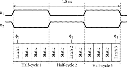
The basic problem with traditional domino circuits is that data must arrive by the end of one half-cycle but will not depart until the beginning of the next half-cycle. Therefore, the circuits must budget skew between the clocks and cannot borrow time. We can overcome this problem by using overlapping clocks, as shown in Figure 1.15. This figure shows a skew-tolerant domino clocking scheme with two overlapping clock phases. Instead of using clk and its complement, we now use overlapping clocks φ1 and φ2. We partition the logic into phases instead of half-cycles because in general we will allow more than two overlapping phases. The clocks overlap enough that even under worst-case clock skews providing minimum overlap, the first gate B in the second phase has time to evaluate before the last gate A in the first phase begins precharge. As with static latches, the gates are guaranteed to be ready to operate when the data arrives even if skews cause modest variation in the arrival time of the clock. Therefore we do not need to budget clock skew in the cycle time.

Another advantage of skew-tolerant domino circuits is that latches are not necessary within the domino pipeline. We ordinarily need latches to hold the result of the first phase’s computation for use by the second phase when the first phase precharges. In skew-tolerant domino, the overlapping clocks insure that the first gate in the second phase has enough time to evaluate before φ1 falls and the first phase begins precharge. When the first phase precharges, the dynamic gates will pull high and therefore the static gates will fall low. This means that the input to the second phase falls low, seemingly violating the monotonicity rule that inputs to dynamic gates must make only low-to-high transitions while the gates are in evaluation. What are the consequences of violating monotonicity? Gate B will remain at whatever value it evaluated to based on the results of the first half-cycle when its inputs fall low because both the pulldown transistors and the precharge transistor will be off. This is exactly what we want: gate B will keep its value even when Phase 1 precharges. Hence, there is no need for a latch at the end of Phase 1 to remember the result during precharge. The entire cycle is available for useful computation; there is no sequencing overhead from latch delay or clock skew:
Finally, skew-tolerant domino circuits can allow time borrowing if the overlap between clock phases is larger than the clock skew. The guaranteed overlap is the nominal overlap minus uncertainty due to the clock skew. Gates in either Phase 1 or Phase 2 may evaluate during the overlap period, allowing time borrowing by letting gates that nominally evaluate during Phase 1 to run late into the second phase. As usual, it is hard to quantify the benefits of time borrowing, but it is clear that the designer has greater flexibility.
In summary, skew-tolerant domino circuits use overlapping clocks to eliminate latches and remove all three sources of overhead that plague traditional domino circuits: clock skew, latch delay, and imbalanced logic. We will see in Section 1.5.2 that this overhead can be about 25% of the cycle time of a well-designed system today and will increase as cycles get shorter. Therefore, skew-tolerant domino is significantly faster than traditional domino in aggressive systems.
Two-phase skew-tolerant domino circuits conveniently illustrate the benefits of skew-tolerant domino design, but prove to suffer from hold time problems and offer limited amounts of time borrowing and skew tolerance. Chapter 3 generalizes the idea to multiple overlapping clock phases and derives formulae describing the available time borrowing and skew tolerance as a function of the number of phases and the duty cycle. Chapter 5 addresses the challenges of producing the multiple overlapping phases.
1.5 Case Studies
To illustrate the benefits of skew-tolerant circuit design, let us consider three brief case studies. The first is an application-specific integrated circuit (ASIC) using static logic and edge-triggered flip-flops in which sequencing overhead got out of hand. The second is the Alpha 21164, a much more aggressive and heavily optimized design in which traditional domino circuits still impose an overhead of about 25% of the cycle time. The third is a study of timing analysis showing how better analysis leads to less pessimistic results. The first two studies come from real industrial projects, while the third is contrived to illustrate the idea in a simple way.
1.5.1 Sequencing Overhead in a Static ASIC
A colleague spent the summer of 1998 designing an application-specific integrated circuit targeting 200 MHz operation in the TSMC 0.25-micron process. Names are withheld to protect the innocent. The process provided an estimated 120 ps fanout-of-4 inverter delay, so the 5 ns cycle time was about 40 FO4 inverter delays. This is reasonably aggressive for a static CMOS ASIC design, but is not unreasonable with careful attention to pipeline partitioning and circuit implementation.
Unfortunately, as is often the case at the forefront of technology, the process was new and untested. As a result, the clock skew budget was set to be ±500 ps. In the notation of this book, tskew = 1000 ps because the launching clock might be skewed late while the receiving clock is skewed early. The cell library included an edge-triggered flip-flop with a total delay of ΔDC + ΔCQ = 400 ps. With these figures, the sequencing overhead consumed 1.4 ns, or 28% of the cycle time, neglecting the further overhead of imbalanced logic. Only 3.6 ns, or 30 FO4 inverter delays, were left for useful logic. Thus the design became much more challenging than it should have been. The conservative estimate of clock skew led to higher engineering costs as the engineer was forced to overdesign the critical paths.
Several approaches could have eased the design. The most effective would have been to use latches rather than flip-flops on the critical paths. This would have removed clock skew from the cycle time budget, relinquishing about 8 FO4 inverter delays for useful computation. Unfortunately, the ASIC house did not have experience with, or tools for, latch-based design, so this was not an option at the time. However, latch-based design has been practiced in the industry for decades and is supported by many CAD packages, so an investment in such capability would provide payoffs on many future high-speed designs.
Another approach would have been to understand the sources and magnitude of the clock skew better. Indeed, late in the design, the skew budget was reduced to 720 ps through better analysis. This offered little solace to the designer who had spent enormous amounts of effort optimizing paths to operate under the original skew budget. Most paths communicate between nearby flip-flops that see much less skew than flip-flops on opposite corners of the die. If such information were made explicit to the analysis tools, the overhead could also be reduced on those paths. We’ll look at this idea more closely in Section 1.5.3 and Chapter 6.
1.5.2 Sequencing Overhead in the Alpha 21164
The Alpha 21164 was the fastest commercial microprocessor of its day, achieving 500 MHz in 1996 using a 0.35-micron process years before most of its competition caught up using 0.18-micron processes. It relied on extensive use of domino circuits to achieve its speed. Traditional two-phase domino was most widely used [26].
We can estimate the sequencing overhead of the domino given a reported clock skew of 200 ps. If we assume the latch setup time is only 50 ps, we find a total of 250 ps of overhead must be budgeted in each half-cycle and 500 ps must be budgeted per cycle. This accounts for 25% of the 2 ns cycle time, neglecting any overhead from imbalanced logic.
The Alpha designers were unwilling to sacrifice this much time to overhead. They used two approaches to reduce the overhead. One was to use overlapping clocks in the ALU self-bypass path to eliminate one of the latches, effectively acting as two-phase skew-tolerant domino. A second was to compute local skews between nearby clocked elements and use these smaller skews wherever possible rather than budgeting global skew everywhere. Data circulating in the ALU self-bypass loop sees only this local skew. At the time of design, standard timing analyzers could not handle different amounts of skew between different latches, so the design team had to use an internal timing analyzer. Now this capability is becoming available in major commercial tools such as Pathmill with the Clock Skew Option.
1.5.3 Timing Analysis with Clock Skew
When clocks experience different amounts of clock skew relative to one another, a good timing analyzer will determine the clocks that launched and terminated a path and allocate only the necessary skew rather than pessimistically budgeting the worst-case skew. To see the difference, consider the path in Figure 1.16 targeting 1 GHz operation. In this path, let us assume that φ1 has only 10 ps of skew relative to other copies of itself, but that φ2 may experience 200 ps of skew relative to φ1· Assume a setup time of 60 ps and a D-to-Q delay of 50 ps for each latch.
Suppose the path from latch 1 to latch 2 is long and borrows 210 ps into half-cycle 2, as shown in the figure. The path from latch 2 to latch 3 is also long. We would like our timing analyzer to tell us if the path will violate the setup time at latch 3. How much clock skew must be budgeted in this path?
At first, we might assume that because there is 200 ps of skew between φ2 and φ1; the data must arrive at latch 3 at a setup time and clock skew before the falling edge of φ2, that is, no later than 1.5 ns – 0.2 ns – 0.06 ns = 1.24 ns. Indeed, at least one commercial timing analyzer reports exactly this.
Looking more closely, we realize that the data arrives at latch 2 while latch 2 is transparent. Therefore, latch 2 does not retime the data departure. The path is launched from latch 1 and must budget only 10 ps of skew at latch 3 because the launching and receiving clocks are both φ1. The true required time at latch 3 is 1.5 ns – 0.01 ns – 0.06 ns = 1.43 ns. By considering the launching and receiving clocks, we determine that we have 190 ps more time available than we might have pessimistically assumed.
Figure 1.17 shows a sample of a report we would like to receive from timing analysis. In this example, we assume the logic delay between latch 2 and latch 3 is 0.6 ns. The report indicates that data departs latch 2 at 0.71 ns relative to φ1. It has a 0.05 ns propagation delay through the latch and 0.60 ns delay through the logic, arriving at latch 3 at 1.36 ns. This requires borrowing 0.36 ns into half-cycle 3. Because the path was launched by φ1 and received by φ1, only 0.01 ns of skew must be budgeted. The maximum time available for borrowing is 0.43 ns, determined by the half-cycle time less the setup and appropriate clock skew. Therefore the path meets the setup time with an acceptable amount of time borrowing. If 0.2 ns of skew were budgeted, the path would miss timing by 120 ps.
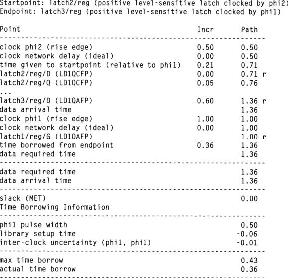
Timing analysis with different amounts of clock skew between different clocks in systems supporting time borrowing is somewhat subtle, as this example has illustrated. The concept of departure times relative to various clocks is developed in Chapter 6, along with algorithms to perform the timing analysis. Be aware that your timing analyzer may not yet support such analysis.
1.6 A Look Ahead
In this chapter we have examined the sources of sequencing overhead and seen that it is a growing problem in high-speed digital circuits, as summarized in Table 1.3. While flip-flops and traditional domino circuits have severe overhead, transparent latches and skew-tolerant domino circuits hide clock skew and allow time borrowing to balance logic between pipeline stages. In the subsequent chapters we will flush out these ideas to present a complete methodology for skew-tolerant circuit design of static and dynamic circuits.
Table 1.3
| Sequencing method | Sequencing overhead |
| Flip-flops | ΔCQ + ΔDC + tskew + imbalanced logic |
| Transparent latches | 2ΔDQ |
| Traditional domino | 2ΔDC + 2tskew + imbalanced logic |
| Skew-tolerant domino | 0 |
Chapter 2 focuses on static circuit design. It examines the three commonly used memory elements: flip-flops, transparent latches, and pulsed latches. While flip-flops clearly have the worst overhead, transparent latches and pulsed latches each have pros and cons. Pulsed latches are faster in an ideal environment, but transparent latches have less critical race conditions and can tolerate more clock skew and time borrowing. We take a closer look at time borrowing and latch placement, then consider hold time violations, which we have ignored in this introduction. Finally, we survey a variety of memory element implementations.
Chapter 3 moves on to domino circuit design. It addresses the question of how to best clock skew-tolerant domino circuits and derives how much skew and time borrowing can be handled as a function of the number of clock phases and their duty cycles. Given these formulae, hold times, and practical clock generation issues, we conclude that four-phase skew-tolerant domino circuits are a good way to build systems. We then return to general domino design issues, including monotonicity, footed and unfooted dynamic gates, and noise.
Chapter 4 puts together static and domino circuits into a coherent skew-tolerant circuit design methodology. It looks at the interface between the two circuit families and shows that the static-to-domino interface must budget clock skew, motivating the designer to build critical rings entirely in domino for maximum performance. It describes the use of timing types to verify proper connectivity in static circuits, then extends timing types to handle skew-tolerant domino. Finally, it addresses issues of testability and shows that scan techniques can serve both latches and skew-tolerant domino in a simple and elegant way.
None of these skew-tolerant circuit techniques would be practical if providing the necessary clocks introduced more skew than the techniques could handle. Chapter 5 addresses clock generation and distribution. Many experienced designers reflexively cringe when they hear schemes involving multiple clocks because it is virtually impossible to route more than one high-speed clock around a chip with acceptable skew. Instead, we distribute a single clock across the chip and locally produce the necessary phases with the final-stage clock drivers. We analyze the skews from these final drivers and conclude that although the delay variation is non-negligible, skew-tolerant circuits are on the whole a benefit. In addition to tolerating clock skew, good systems minimize the skew that impacts each path. By considering the components of clock skew and dividing a large die into multiple clock domains, we can budget smaller amounts of skew in most paths than we must budget across the entire die.
By this point, we have developed all the ideas necessary to build fast skew-tolerant circuits. With a little practice, skew-tolerant circuit design is no harder than conventional techniques. However, it is impossible to build multimillion transistor ICs unless we have tools that can analyze and verify our circuits. In particular, we need to be able to check if our circuits can meet timing objectives given the actual skews between clocks in various domains. Chapter 6 addresses this problem of timing analysis, extending previous formulations to handle multiple domains of clock skew.
By the end of this book, you should have a thorough understanding of how to design skew-tolerant static and domino circuits. Although such design is not difficult, it has been ignored by the bulk of engineers and computer-aided design systems because flip-flops were adequate when cycle times were long and thus sequencing overhead was small. High-end microprocessors push circuit performance to the limit and will benefit from skew-tolerant domino circuits to reduce overhead. Application-specific integrated circuits will generally have less aggressive frequency targets and are unlikely to employ domino circuits until signal integrity tools improve. Nevertheless, many ASICs will be fast enough that flip-flop overhead becomes significant, and a switch to skew-tolerant latches may make design easier. Given these trends, skew-tolerant circuit design should be an exciting area in the coming years.
1.7 Exercises
[15] 1.1. You are building the AlphaNot microprocessor and plan to use flip-flops as your state elements. Suppose the setup and clock-to-Q delays of the flip-flops are 1.5 FO4 delays each. Assume there is no clock skew. You are targeting a 0.18-micron process with a 60 ps FO4 inverter delay. If the operating frequency is to be 600 MHz, what fraction of the cycle time is wasted for sequencing overhead? Repeat if the operating frequency is 1 GHz.
[15] 1.2. Repeat Exercise 1.1 if the clock skew is 150 ps.
[15] 1.3. Repeat Exercise 1.1 using transparent latches instead of flip-flops. Your latches have setup and clock-to-Q delays of 1.5 FO4 delays each. They have a D-to-Q delay of 1.3 FO4 delays.
[15] 1.4. Repeat Exercise 1.3 if the clock skew is 150 ps.
[15] 1.5. You are designing an IEEE single-precision floating-point multiplier targeting 200 MHz operation in a 0.18-micron process using synthesized static CMOS logic and conventional flip-flops. The flip-flops in your cell library have a setup time of 200 ps and a clock-to-Q delay of 300 ps for the expected loading. You are budgeting clock skew of 400 ps. How much time (in nanoseconds) is available for useful multiplier logic?
[15] 1.6. Repeat Exercise 1.5 if you are using IBM’s 0.16-micron SA-27 process using synthesized static CMOS logic and conventional flip-flops. An excerpt from IBM’s cell library data book is shown in Figure 1.18. Assume you will use the LDE0001 flip-flop (ignore the A, B, C, and I inputs used for level-sensitive scan) in the E performance level driving a load of four standard loads. Extract the maximum setup time and clock-to-Q (i.e., E-L2) delays from the data sheet assuming worst-case process and environment.
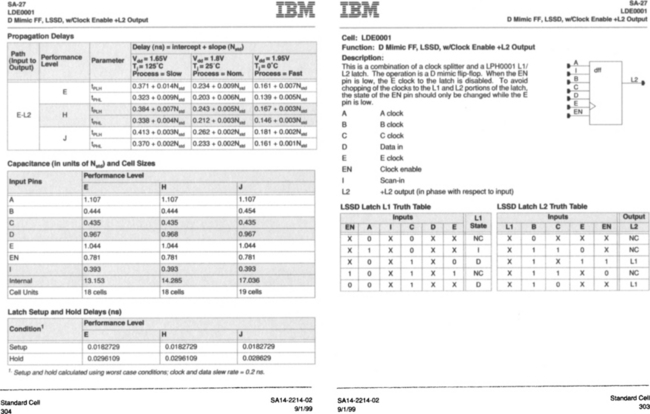
Figure 1.18 Excerpt from IBM SA-27 0.16-micron cell library data book (Reproduced by permission from http://www.chips.ibm.com/techlib/products/asics/databooks.html.) Copyright 2001 by International Business Machines.
[20] 1.7. You are building the Motoroil 68W86 processor for embedded automotive applications. Suppose your system is built using flip-flops with ΔDC = 100 ps and ΔCQ = 120 ps and that there is no clock skew. Your computation requires 3 ns to complete. You are considering various pipeline organizations in which the computation is done in 1, 2, 3, or 4 clock cycles in the hopes that breaking the computation into multiple cycles would allow a faster clock rate. Make a table showing the maximum possible clock frequency for each option. Also show the total latency of the computation (in picoseconds) for each option.
[15] 1.8. In Exercise 1.7 we assumed that logic could be divided into any number of cycles without waste. In practice, you may have time remaining at the end of a cycle for half a gate delay; this time goes unused because it is impossible to build half a gate. Redo the exercise if on average 50 ps at the end of each cycle goes unused due to imbalanced logic.
[10] 1.9. Why is sequencing overhead a more important concern to designers in the year 2000 than it was in 1990?
[35] 1.10. Gather data to extend the plots in Figures 1.3 and 1.4 from 1995 to the present. How fast is microprocessor performance increasing? How about clock rate? How long does it take for performance to double? Clock rate? Have these trends accelerated or decelerated relative to the performance increases between 1985 and 1997? How do they compare with the SIA roadmap in Table 1.2?
[10] 1.11. Why are domino circuits faster than static CMOS circuits?
[15] 1.12. You are designing the Pentagram IV Processor. Consider using a pipeline built with traditional domino circuits. The pipeline requires 1 ns of logic in each cycle. Suppose the setup time of each latch is 90 ps and the clock skew is 100 ps. What is the cycle time? What fraction of the cycle is lost to sequencing overhead?
[15] 1.13. Repeat Exercise 1.12 if the system is built from two-phase skew-tolerant domino circuits.
[20] 1.14. You are developing a circuit methodology for an ultra-high-speed processor. You are weighing whether to recommend static CMOS circuits or traditional domino circuits. You have determined that the setup time and D-to-Q delay of your latches are approximately equal. You determined that the ALU self-bypass path is a key cycle-limiting path with a logic delay of Δlogic if you construct it with static CMOS circuits. If you use domino circuits, you determine it will require only 0.7 Δlogic but you must also budget clock skew. Figure 1.19 shows a design space of logic delay and clock skew. Divide the space into two regions based on whether static CMOS or traditional domino circuits offer higher operating frequencies for the given logic delay and skew. Assume there is no imbalanced logic.
[15] 1.15. Repeat Exercise 1.14 assuming that there is 0.25 FO4 delays of time wasted on average from imbalanced logic in the traditional domino design.
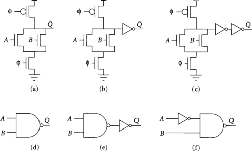
[10] 1.16. Which of the circuits in Figure 1.20 produce outputs Q that can correctly drive a domino gate that evaluates on φ? Assume the inputs A and B to each circuit are monotonically rising while φ is high. The NAND and NOT gates are built from static CMOS.
[15] 1.17. Define “hard edges” as used in this chapter in your own words. Which of the following pipeline design approaches introduce hard edges: static CMOS with flip-flops, static CMOS with transparent latches, traditional domino circuits, skew-tolerant domino circuits? Why do hard edges reduce performance?