
Clocking
Clocking is a key challenge for high-speed circuit designers. Circuit designers specify a modest number of logical clocks that ideally arrive at all points on the chip at the same time. For example, flip-flop-based systems use a single logical clock, while skew-tolerant domino might use four logical clocks. Unfortunately, mismatched clock network paths and processing and environmental variations make it impossible for all clocks to arrive at exactly the same time, so the designer must settle for actually receiving a multitude of skewed physical clocks. To achieve low clock skew, it is important to carefully match all of the paths in the clock network and to minimize the delay through the network because random variations lead to skews that are a fraction of the mismatched delays. Previously, we have focused on hiding skew where possible and budgeting where necessary. We must be careful, however, that our skew-tolerant circuit techniques do not complicate the clock network so much that they introduce more skew than they tolerate.
This chapter begins by defining the nominal waveforms of physical clocks. The interarrival time of two clock edges is the delay between the edges. Clock skew is the absolute difference between the nominal and actual interarrival times of a pair of physical clock edges. Clock skew displays both spatial and temporal locality; by considering such locality, we must budget or hide only the actual skew experienced between launching and receiving clocks of a particular path. Skew budgets for min-delay checks must be more conservative than for max-delay because of the dire consequences of hold time violations; fortunately, min-delay races are set by pairs of clocks sharing a common edge in time, so min-delay budgets need not include jitter or duty cycle variation. Because it may be impractical to tabulate the skew between every pair of physical clocks on a chip, we lump clocks into domains for simplified, though conservative, analysis.
Having defined clock skew, we turn to skew-tolerant domino clock generation schemes for two, four, and more phases. We see that the clock generators introduce additional delays into the clock network and hence increase clock skew. Nevertheless, the extra clock skew is small compared to the skew tolerance, so such generators are acceptable. Four-phase skew-tolerant domino proves to be a reasonable design point combining good skew tolerance and simple clock generation, so we present a complete four-phase clock generation network supporting clock enabling and scan.
5.1 Clock Waveforms
We have relied upon an intuitive definition of clock skew while discussing skew-tolerant circuit techniques. In this chapter, we will develop a more precise definition of clock skew that takes advantage of the myriad correlations between physical clocks. Physical clocks may have certain systematic timing offsets caused by different numbers of clock buffers, clock gating, and so on. We can plan for these systematic offsets by placing more logic in some phases and less in others than we would have if all physical clocks exactly matched the logical clocks; the nominal offsets between physical clocks do not appear in our skew budget. The only term that must be budgeted as skew is the variability, the difference between nominal and actual interarrival times of physical clocks.
5.1.1 Physical Clock Definitions
A system has a small number of logical clocks. For example, flip-flops or pulsed latches use a single logical clock, transparent latches use two logical clocks, and skew-tolerant domino uses N, often four, logical clocks. A logical clock arrives at all parts of the chip at exactly the same time. Of course logical clocks do not exist, but they are a useful fiction to simplify design.
Conceptually, we envision a unique physical clock for each latch, but we can quickly group physical clocks that represent the same logical clock and have very small skew relative to each other into one clock to reduce the number of physical clocks. For example, a single physical clock might serve a bank of 64 latches in a datapath. By defining waveforms for physical clocks rather than logical clocks, we set ourselves up to budget only the skew actually possible between a pair of physical clocks rather than the worst-case skew experienced across the chip.
We define the set of physical clocks to be C = {φ1, φ2, …, φk}. We assume that all clocks have the same cycle time Tc.1 Variables describing the clock waveforms are defined below and illustrated in Figure 5.1 for a two-phase system with four 50% duty cycle physical clocks.
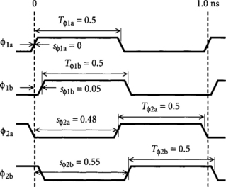
![]() Tc: the clock cycle time, or period
Tc: the clock cycle time, or period
![]() Tφi: the duration for which φi is high
Tφi: the duration for which φi is high
![]() Sφi: the start time, relative to the beginning of the common clock cycle, of φi being high
Sφi: the start time, relative to the beginning of the common clock cycle, of φi being high
![]() Sφi φ j: a phase shift operator describing the difference in start time from φi to the next occurrence of φj.
Sφi φ j: a phase shift operator describing the difference in start time from φi to the next occurrence of φj. ![]() where Wis a wraparound variable indicating the number of cycle crossings between the sending and receiving clocks. W is 0 or 1 except in systems with multicycle paths. Note that
where Wis a wraparound variable indicating the number of cycle crossings between the sending and receiving clocks. W is 0 or 1 except in systems with multicycle paths. Note that ![]() = −Tc because it is the shift between consecutive rising edges of clock phase φi.
= −Tc because it is the shift between consecutive rising edges of clock phase φi.
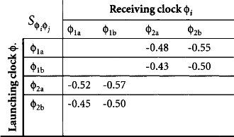
Note that Figure 5.1 labels the clocks C = {φ1a, φ1b, φ2a, φ2b} rather than C = {φ1, φ2, φ3 φ4} to emphasize that the four physical clocks correspond to only two logical clocks. The former labeling will be used for examples, while the latter notation is more convenient for expressing constraints in timing analysis in Chapter 6. The phase shifts between these clocks seen at consecutive transparent latches are shown in Table 5.1. Notice that the systematic offsets between clocks appear as different phase shifts rather than clock skew. It is possible to design around such systematic offsets, intentionally placing more logic in one half-cycle than another. Indeed, designers sometimes intentionally delay clocks to extend critical cycles of logic in flip-flop-based systems where time borrowing is not possible. We save the term “skew” for uncertainties in the clock arrival times.
5.1.2 Clock Skew
If the actual delay between two phases φi and φj equalled the nominal delay ![]() the phases would have zero skew. Of course, delays are seldom nominal, so we must define clock skew. There are many sources of clock skew. When a single physical clock serves multiple clocked elements, delay between the clock arrivals at the various elements appears as skew. Cross-die variations in processing, temperature, and voltage also lead to skew. Electromagnetic coupling and load capacitance variations [18] lead to further skew in a data-dependent fashion. If all clock paths sped up or slowed down uniformly, the interarrival times would be unaffected and no skew would be introduced. Therefore, we are only concerned with differences between delays in the clock network.
the phases would have zero skew. Of course, delays are seldom nominal, so we must define clock skew. There are many sources of clock skew. When a single physical clock serves multiple clocked elements, delay between the clock arrivals at the various elements appears as skew. Cross-die variations in processing, temperature, and voltage also lead to skew. Electromagnetic coupling and load capacitance variations [18] lead to further skew in a data-dependent fashion. If all clock paths sped up or slowed down uniformly, the interarrival times would be unaffected and no skew would be introduced. Therefore, we are only concerned with differences between delays in the clock network.
In previous chapters, we have used a single skew budget tskew that is the worst-case skew across the chip, in other words, the largest absolute value of the difference between the nominal and actual interarrival times of a pair of clocks anywhere on the chip. When tskew can be held to about 10% of the cycle time, it is simple and not overly limiting to budget this worst-case skew everywhere. As skews are increasing relative to cycle time, we would prefer to only budget the actual skew encountered on a path, so we define skews between specific pairs of physical clocks. For example, ![]() is the skew between φi and φj, the absolute value of the difference between the nominal and actual interarrival times of these edges measured at any pair of elements receiving these clocks. For a given pair of clocks, certain transitions may have different skews than others. Therefore, we also define skews between particular edges of pairs of physical clocks. For example,
is the skew between φi and φj, the absolute value of the difference between the nominal and actual interarrival times of these edges measured at any pair of elements receiving these clocks. For a given pair of clocks, certain transitions may have different skews than others. Therefore, we also define skews between particular edges of pairs of physical clocks. For example, ![]() is the skew between the rising edge of φi and the falling edge of φj·
is the skew between the rising edge of φi and the falling edge of φj· ![]() is the maximum of the skews between any edges of the clocks.
is the maximum of the skews between any edges of the clocks.
Notice that skew is a positive difference between the actual and nominal interarrival times, rather than being plus or minus from a reference point. When using this information in a design, we assume the worst: for maximum-delay (setup time) checks, that the receiving clock is skewed early relative to the launching clock; and for minimum-delay (hold time) checks, that the receiving clock is skewed late relative to the launching clock. If skews are asymmetric around the reference point, we may define separate values of skew for min- and max-delay analysis.
Also, note that the cycle count between edges is important in defining skew. For example, the skew between the rising edge of a clock and the same rising edge a cycle later is called the cycle-to-cycle jitter. The skew between the rising edge and the same rising edge many cycles later may be larger and is called the peak jitter. Generally, we will only consider edges separated by at most one cycle when defining clock skew because including peak jitter is overly pessimistic. This occasionally leads to slightly optimistic results in latch-based paths in which a signal is launched on the rising edge of one latch clock and passes through more than one cycle of transparent latches before being sampled. The jitter between the launching and sampling clocks is greater than cycle-to-cycle jitter in such a case, but the error is unlikely to be significant.
Since clock skew depends on mismatches between nominally equal delays through the clock network, skews budgets tend to be proportional to the absolute delay through the network. Skews between clocks that share a common portion of the clock network are smaller than skews between widely separated clocks because the former clocks experience no environmental or processing mismatches through the common section. However, even two latches sharing a single physical clock experience cycle-to-cycle skew from jitter and duty cycle variation, which depend on the total delay through the clock network.
The designer may use different skew budgets for minimum- and maximum-delay analysis purposes. Circuits with hold time problems will not operate correctly at any clock frequency, so designers must be very conservative. Fortunately, min-delay races occur between clocks in a single cycle, so jitter and duty cycle variation are not part of the skew budget. Circuits with setup time problems operate properly at reduced frequency. Therefore, the designer may budget an expected skew, rather than a worst-case skew, for max-delay analysis, just as designers may target TT processing instead of SS processing. This avoids overdesign while achieving acceptable yield at the target frequency. Unfortunately, calculating the expected skew requires extensive statistical knowledge of the components of clock skew and their correlations.
On account of larger chips, greater clock loads, and wire delays that are not scaling as well as gate delays, it is very difficult to hold clock skew across the die constant in terms of gate delays. Indeed, Horowitz predicted that keeping global skews under 200 ps is hard [39]. Moreover, as cycle times measured in gate delays continue to shrink, even if clock skew were held constant in gate delays, it would tend to become a larger fraction of the cycle time. Therefore, it will be very important to take advantage of skew-tolerant circuit techniques and to exploit locality of clock skew when building fast systems.
5.1.3 Clock Domains
Although you may conceptually specify an array of clock skews between each pair of physical clocks in a large system, such a table may be huge and mostly redundant. In practice, designers usually lump clocks into a hierarchy of clock domains. For example, we have intuitively discussed local and global clock domains; pairs of clocks in a particular local domain experience local skew, which is smaller than the global skew seen by clocks in different domains. We can extend this notion to finer granularity by defining a skew hierarchy with more levels of clock domains, as shown in Figure 5.2 for a system based on an H-tree.
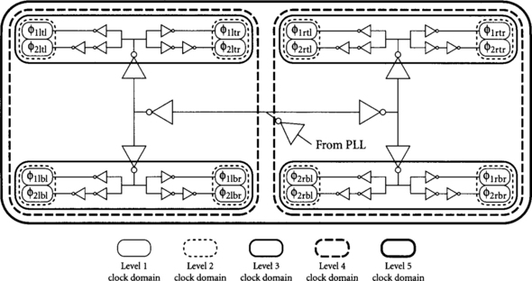
In Figure 5.2, level 1 clock domains contain a single physical clock. Therefore, two elements in the level 1 domain will only see skew from RC delays along the clock wire and from jitter of the physical clock. Level 2 clock domains contain a clock and its complement and see additional skew caused by differences between the nominal and actual clock generator delays. Remember that systematic delay differences that are predictable at design time can be captured in the physical clock waveforms; only delay differences from process variations or environmental differences between the clock generators appear as skew. Higher-level clock domains see progressively more skew as delay variations in the global clock distribution network appear as skew.
5.2 Skew-Tolerant Domino Clock Generation
In most high-frequency systems, a single clock gclk is distributed globally using a modified H-tree or grid to minimize skew. Skew-tolerant domino can use this same clock distribution scheme with a single global clock. Within each unit or functional block, local clock generators produce the multiple phases required for latches and skew-tolerant domino. These local generators inevitably increase the delay of the distribution network and hence increase clock skew. This section describes several local clock generation schemes and analyzes the skews introduced by the generators. The simplest schemes involve simple delay lines and are adequate for many applications. Lower skews can be achieved using feedback systems with delays that track with process and environmental changes. We conclude with a full-featured local clock generator supporting transparent latches and four-phase skew-tolerant domino, clock enabling, and scan.
5.2.1 Delay Line Clock Generators
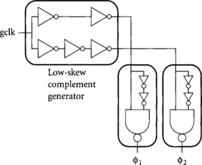
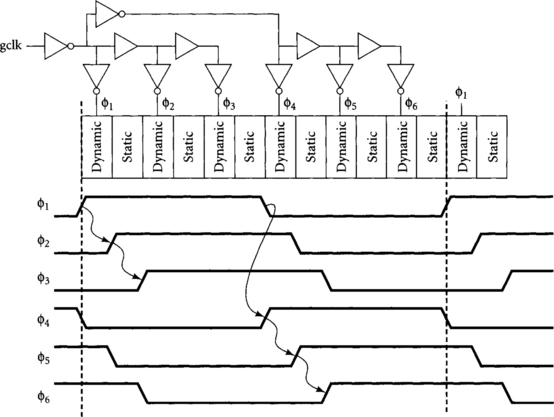
Overlapping clocks for skew-tolerant domino can be easily generated by delaying one or both edges of the global clock with chains of inverters. Figure 5.3 shows a simple two-phase skew-tolerant domino local generator, while Figure 5.4 extends the design to support four phases. The two-phase design uses a low-skew complement generator to produce complementary signals from the global clock. For example, Shoji showed how to match the delay of two and three inverters independently of relative PMOS/NMOS mobilities [78]. The falling clock edges are stretched with clock choppers to produce waveforms with greater than 50% duty cycle. Using a fanout of 3–4 on each inverter delay element sets reasonable delay and minimizes the area of the clock buffer while preserving sharp clock edges.
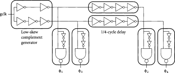
The four-phase design is very similar, but uses an additional chain of inverters to produce a nominal quarter-cycle delay. At first it would seem such a clock generator would suffer from terrible clock skews because between best- and worst-case processing and environment, its delay may vary by a factor of two! Fortunately, we are concerned not with the absolute delay of the inverter chain, but rather with its tracking relative to critical paths on the chip. In the slow corner, the delay chain will have a greater delay, but the critical paths will also be slower and the operating frequency will be correspondingly reduced. Hence, to first order, the delay chain tracks the speed of the logic on the chip; we are now concerned about skew introduced by second-order mismatches.
Local-Generator-Induced Clock Skew
Since the local generators are not replicas of the circuits they are tracking, and indeed are static gates tracking the speed of dynamic paths, their relative delays may vary over process corners as well as due to local variation in voltage, temperature, and processing. Simulation finds that when most of the chip is operating under nominal processing and worst-case environment but a local clock generator sees a temperature 30°C lower and supply voltage 300 mV higher, the local generator will run 13% faster than nominal (6% from temperature, 7% from voltage). The relative delay of simple domino gates with respect to FO4 inverters varies up to about 6% across process corners. Finally, process tilt (i.e., fluctuation in Le, tox, etc., across the die) may speed the local clock generator more than nearby logic. Little data is available on process tilt, but if we guess it causes a similar 13% variation, we conclude that nearly a third of the total local clock generator delay appears as clock skew.
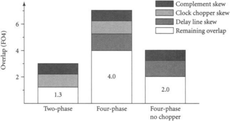
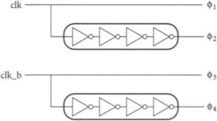
Four-phase clock generators have a quarter-cycle more delay than two-phase generators, so are subject to more skew. However, they can also tolerate a quarter-cycle more skew than their two-phase counterparts, which is significantly more than the extra skew of the generators. For example, consider two- and four-phase systems like those described in Section 3.1.2 with cycle times of 16 FO4 delays and precharge times of 4 FO4 delays. If the local skew is 1 FO4 delay, the nominal overlap between phases is 3 FO4 delays for the two-phase system and 7 FO4 delays for the four-phase system. These overlaps can be used to tolerate clock skew and allow time borrowing. From the overlap we must subtract the skews introduced by the local clock generators. If the complement generator, clock chopper, and quarter-cycle delay lines have nominal delays of 2, 3, and 4 FO4 delays, respectively, we must budget 32% of these delays as additional skew. Figure 5.5 compares the remaining overlaps of each system, showing that although the four-phase system pays a larger skew penalty, the remaining overlap is proportionally much greater than that of the two-phase system. The four-phase clock generator can be simplified to use 50% duty cycle clocks as shown in Figure 5.6, eliminating the clock choppers at the expense of smaller overlaps. The four-phase system with 50% duty cycle waveforms still provides more overlap than the two-phase system and avoids the min-delay problems associated with overlapping two-phase clocks. Therefore, it is a reasonable design choice, especially considering the drawbacks of clock choppers that we will shortly note. In Section 5.2.3 we will look at a complete four-phase clock generator including clock gating and scan capability.
The four-phase clock generator with clock choppers appears to offer substantial benefits over the design with no choppers. A closer look reveals several liabilities in the design with choppers. Variations in the clock chopper delay cause duty cycle errors that cut into the precharge time, necessitating smaller overlaps than our first-order analysis predicted. The extended duty cycle also increases the susceptibility to min-delay problems, especially when coupled with the large skews introduced by the clock generator. Finally, the designer may still desire to use 50% duty cycle clocks for transparent latches. Therefore, the chopperless four-phase scheme is preferred when it offers enough overlap to handle the expected skews and time-borrowing requirements.
In addition to having adequate overlap for time borrowing and hiding clock skew, domino clocks must have sufficiently long precharge times in all process corners. The local clock generators are subject to duty cycle variation, which might change the amount of time available for precharging. Fortunately, if we design the system to have adequate precharge time in the worst-case environment under TT processing, environmental changes will only lead to more precharge time and faster precharge operation. In the SS corner, the clock must be slowed to accommodate precharge, but it is slowed anyway because of the longer critical paths.
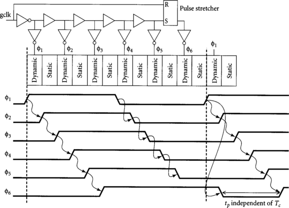
N-Phase Local Clock Generators
Another popular skew-tolerant domino clocking scheme is to provide one phase for each gate. This offers maximum skew tolerance and more precharge time, as discussed in Section 3.1.4, at the expense of generating and distributing more clocks and roughly matching gate and clock delays. Figures 5.7 and 5.8 show such clock generation schemes. Figure 5.7 uses both edges of the clock and is the simplest scheme. The exact delay of the buffers is not particularly important so long as the clocks arrive at each gate before the data. Figure 5.8 delays a single clock edge, as used on the IBM guTS experimental GHz processor [62, 86], its successor [38], and on the Sun UltraSparc III [32]. To make sure the last phase overlaps the first phase of the next cycle, a pulse stretcher, such as an SR latch, must be used. The stretcher is especially important at low frequency; the first guTS test chip accidentally omitted a stretcher, making the chip only run at a narrow range of frequencies. Another disadvantage of delaying a single edge is that the precharge time of the last phase becomes independent of clock frequency, creating another timing constraint that cannot be fixed by slowing the clock. Finally, the longer delays of the single-edge design lead to greater clock skew. Therefore, the design delaying both edges is simpler and more robust.
5.2.2 Feedback Clock Generators
To reduce the skew and duty cycle uncertainty of the local clock generators, we may also use local delay-locked loops [14] to produce skew-tolerant domino clocks. Such a system is shown in Figure 5.9. The local loop receives the global clock and delays it by exactly one quarter-cycle by adjusting a delay line to have a half-cycle delay and tapping off the middle of the delay line. The feedback controller compensates for process and low-frequency environmental variations and even for a modest range of different clock frequencies. The art of DLL design is beyond the scope of this work; the illustration should be considered conceptual only.
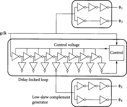
Unfortunately, the DLL itself introduces skew. In particular, power supply noise in the delay line at frequencies above the controller bandwidth appears as jitter on φ2 and φ4. In a system without feedback, power supply variation from V + ΔV to V – ΔV causes delay variation from t + Δt to t – Δt. In the DLL, a supply step from V + ΔV to V – ΔV after the system had initially stabilized at V + ΔV causes delay variation from t to t – 2Δt. Similarly, a rising step causes delay variation from t to t + 2Δt. Therefore, the DLL has twice the voltage sensitivity of the system without feedback. PLLs are even more sensitive to voltage noise because they accumulate jitter over multiple cycles; therefore, they are not a good choice for local clock generators.
Fortunately, the local high-frequency voltage noise causing jitter is a fraction of the total voltage noise. If we assume the high-frequency noise in each DLL is half as large as the total voltage noise, the jitter of the DLL will equal the skew introduced by voltage errors on a regular delay line system. Using the numbers from the example in Section 5.2.1, this corresponds to 7% of the quarter-cycle delay to the line tap. The local clock generator also is subject to variations in the complement generator. If the DLL is designed to achieve negligible static phase offset, the skew improvement of the feedback system over the delay line system is predicted to be the difference in delay sensitivity, 32% – 7%, times the quarter cycle delay, or about 6% of the cycle time. This comes at the expense of building a small DLL in every local clock generator. The DLL may use an improved delay element with reduced supply sensitivity, but the same delay elements may be used in ordinary delay lines. The designer must weigh the potential skew improvement of DLL-based clock generators against the area, power, and design complexity they introduce. In today’s systems, simple delay lines are probably good enough, but in future systems with even tighter timing margins, DLLs may offer enough advantages to justify their costs.
5.2.3 Putting It All Together
So far we have only considered generating periodic clock waveforms. Most systems also require the ability to stop the clock and to scan data in and out of each cycle. We saw in Section 4.3.2 that scan required precise release of the scan enable signal. By building the release circuitry into the clock generator, we avoid the need to route timing-critical global scan signals. In this section we integrate such scan circuitry and clock enabling with four-phase skew-tolerant domino to illustrate a complete local clock generator.
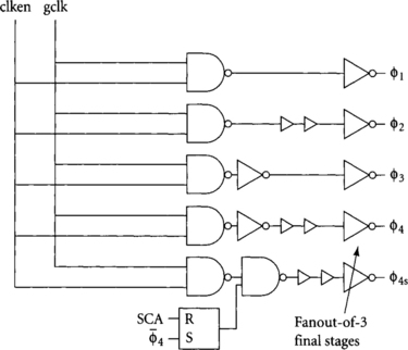
Local clocks are often gated with an enable signal to produce a qualified clock. Qualified clocks can be used to save power by disabling inactive units, to prevent latching new data during a pipeline stall, or to build combined multiplexer-latches. Clock enable signals are often critical because they come from far away or are data dependent. Therefore, it is useful to minimize the setup time of the clock enable before the clock edge.
Figure 5.10 illustrates a complete local clock generator for a four-phase skew-tolerant domino system. It receives gclk from global clock distribution network and an enable signal for the local logic block. It generates the four regular clock phases along with a variant of φ4 used for scan. Different clock enables can be used for different gates or banks of gates as appropriate. Using a two-input NAND gate in all local clock generators provides best matching between phases to minimize clock skew; the enable may be tied high on some clocks that never stop. The last domino gate in each cycle uses φ4 for precharge and φ4s for evaluation. Two-phase static latches use φ1 and φ3 as clk and clk_b. The clock generator uses delay chains to produce domino phases φ2 and φ4 delayed by one quarter of the nominal clock period. Scan is built into static latches and domino gates as described in Section 4.3. Notice that when SCA is asserted, an SR latch forces φ4s low to disable the dynamic gate being scanned. When φ4 falls to begin precharge, the SR latch releases φ4s to resume normal operation. Therefore, we avoid distributing any high-speed global scan enable signals and can use exactly the same scan procedure as we used with static latches:
5.3 Summary
Circuit designers wish to receive a small number of logical clocks simultaneously at all points of the die. They must instead accept a huge number of physical clocks arriving at slightly different times to different receivers. Clock skew is the difference between the nominal and actual interarrival times of two clocks. It depends on numerous sources that are difficult or impossible to model accurately, so it is typically budgeted using conservative engineering estimates. Because clock skew is an increasing problem, it is important to understand the sources and avoid unnecessary conservatism. Skew budgets therefore may depend on the phases of and distance between the physical clocks, the particular edges of the clocks, and the number of cycles between the edges. Clocks may be grouped into a hierarchy of clock domains according to their relative skews; communication within a domain experiences less skew than communication across domains.
The designer has three tactics to deal with skew: budget, hide, and minimize. Taking advantage of the smaller amounts of skew between nearby elements is a powerful way to minimize skew, but requires improved timing analysis algorithms, which are the subject of Chapter 6.
Skew-tolerant circuit techniques hide clock skew, but the local clock generators necessary to produce multiple overlapping clock phases for skew-tolerant domino introduce skew of their own. Fortunately, the skews introduced are less than the tolerance provided, so skew-tolerant domino is an overall improvement.
5.4 Exercises
[15] 5.1. What is the distinction between physical and logical clocks? How many logical clocks exist in Figure 5.2? How many physical clocks?
[15] 5.2. Why is it useful to distinguish between systematic and random variations in the start time of two physical clocks corresponding to the same logical clock? How can the designer use this information to avoid being overly pessimistic in design?
[15] 5.3. What are some advantages of separately defining skews between pairs of clocks rather than providing a single global skew number? What are some disadvantages?
[15] 5.4. Why is the pulse stretcher in Figure 5.8 required? Draw a timing diagram to explain how the circuit might fail if the pulse stretcher were omitted.
[15] 5.5. What is the function of the SR latch in Figure 5.10? Why is it preferable to use the SR latch rather than providing a special scan enable signal to the second NAND gate in the φ4s generator?
[15] 5.6. Many CAD papers describe algorithms for generating “zero-skew” clock trees (e.g., [88]). What is misleading about the term “zero-skew” from the designer’s point of view? What term would you use instead?
1In extremely fast systems, clocks may operate at very high frequency in local areas, but at lower frequency when communicating between remote units. We presently see this in systems where the CPU operates at high speed but the motherboard operates at a fraction of the frequency. This clocking analysis may be generalized to clocks with different cycle times.