
ARM PROCESSOR FUNDAMENTALS
Chapter 1 covered embedded systems with an ARM processor. In this chapter we will focus on the actual processor itself. First, we will provide an overview of the processor core and describe how data moves between its different parts. We will describe the programmer’s model from a software developer’s view of the ARM processor, which will show you the functions of the processor core and how different parts interact. We will also take a look at the core extensions that form an ARM processor. Core extensions speed up and organize main memory as well as extend the instruction set. We will then cover the revisions to the ARM core architecture by describing the ARM core naming conventions used to identify them and the chronological changes to the ARM instruction set architecture. The final section introduces the architecture implementations by subdividing them into specific ARM processor core families.
A programmer can think of an ARM core as functional units connected by data buses, as shown in Figure 2.1, where, the arrows represent the flow of data, the lines represent the buses, and the boxes represent either an operation unit or a storage area. The figure shows not only the flow of data but also the abstract components that make up an ARM core.
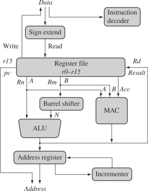
Data enters the processor core through the Data bus. The data may be an instruction to execute or a data item. Figure 2.1 shows a Von Neumann implementation of the ARM—data items and instructions share the same bus. In contrast, Harvard implementations of the ARM use two different buses.
The instruction decoder translates instructions before they are executed. Each instruction executed belongs to a particular instruction set.
The ARM processor, like all RISC processors, uses a load-store architecture. This means it has two instruction types for transferring data in and out of the processor: load instructions copy data from memory to registers in the core, and conversely the store instructions copy data from registers to memory. There are no data processing instructions that directly manipulate data in memory. Thus, data processing is carried out solely in registers.
Data items are placed in the register file—a storage bank made up of 32-bit registers. Since the ARM core is a 32-bit processor, most instructions treat the registers as holding signed or unsigned 32-bit values. The sign extend hardware converts signed 8-bit and 16-bit numbers to 32-bit values as they are read from memory and placed in a register.
ARM instructions typically have two source registers, Rn and Rm, and a single result or destination register, Rd. Source operands are read from the register file using the internal buses A and B, respectively.
The ALU (arithmetic logic unit) or MAC (multiply-accumulate unit) takes the register values Rn and Rm from the A and B buses and computes a result. Data processing instructions write the result in Rd directly to the register file. Load and store instructions use the ALU to generate an address to be held in the address register and broadcast on the Address bus.
One important feature of the ARM is that register Rm alternatively can be preprocessed in the barrel shifter before it enters the ALU. Together the barrel shifter and ALU can calculate a wide range of expressions and addresses.
After passing through the functional units, the result in Rd is written back to the register file using the Result bus. For load and store instructions the incrementer updates the address register before the core reads or writes the next register value from or to the next sequential memory location. The processor continues executing instructions until an exception or interrupt changes the normal execution flow.
Now that you have an overview of the processor core we’ll take a more detailed look at some of the key components of the processor: the registers, the current program status register (cpsr), and the pipeline.
2.1 REGISTERS
General-purpose registers hold either data or an address. They are identified with the letter r prefixed to the register number. For example, register 4 is given the label r4. Figure 2.2 shows the active registers available in user mode—a protected mode normally used when executing applications. The processor can operate in seven different modes, which we will introduce shortly. All the registers shown are 32 bits in size.
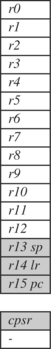
There are up to 18 active registers: 16 data registers and 2 processor status registers. The data registers are visible to the programmer as r0 to r15.
The ARM processor has three registers assigned to a particular task or special function: r13, r14, and r15. They are frequently given different labels to differentiate them from the other registers.
In Figure 2.2, the shaded registers identify the assigned special-purpose registers:
![]() Register r13 is traditionally used as the stack pointer (sp) and stores the head of the stack in the current processor mode.
Register r13 is traditionally used as the stack pointer (sp) and stores the head of the stack in the current processor mode.
![]() Register r14 is called the link register (lr) and is where the core puts the return address whenever it calls a subroutine.
Register r14 is called the link register (lr) and is where the core puts the return address whenever it calls a subroutine.
![]() Register r15 is the program counter (pc) and contains the address of the next instruction to be fetched by the processor.
Register r15 is the program counter (pc) and contains the address of the next instruction to be fetched by the processor.
Depending upon the context, registers r13 and r14 can also be used as general-purpose registers, which can be particularly useful since these registers are banked during a processor mode change. However, it is dangerous to use r13 as a general register when the processor is running any form of operating system because operating systems often assume that r13 always points to a valid stack frame.
In ARM state the registers r0 to r13 are orthogonal—any instruction that you can apply to r0 you can equally well apply to any of the other registers. However, there are instructions that treat r14 and r15 in a special way.
In addition to the 16 data registers, there are two program status registers: cpsr and spsr (the current and saved program status registers, respectively).
The register file contains all the registers available to a programmer. Which registers are visible to the programmer depend upon the current mode of the processor.
2.2 CURRENT PROGRAM STATUS REGISTER
The ARM core uses the cpsr to monitor and control internal operations. The cpsr is a dedicated 32-bit register and resides in the register file. Figure 2.3 shows the basic layout of a generic program status register. Note that the shaded parts are reserved for future expansion.
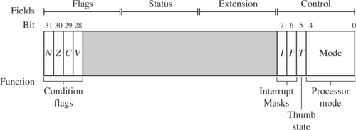
The cpsr is divided into four fields, each 8 bits wide: flags, status, extension, and control. In current designs the extension and status fields are reserved for future use. The control field contains the processor mode, state, and interrupt mask bits. The flags field contains the condition flags.
Some ARM processor cores have extra bits allocated. For example, the J bit, which can be found in the flags field, is only available on Jazelle-enabled processors, which execute 8-bit instructions. We will discuss Jazelle more in Section 2.2.3. It is highly probable that future designs will assign extra bits for the monitoring and control of new features.
For a full description of the cpsr, refer to Appendix B.
2.2.1 PROCESSOR MODES
The processor mode determines which registers are active and the access rights to the cpsr register itself. Each processor mode is either privileged or nonprivileged: A privileged mode allows full read-write access to the cpsr. Conversely, a nonprivileged mode only allows read access to the control field in the cpsr but still allows read-write access to the condition flags.
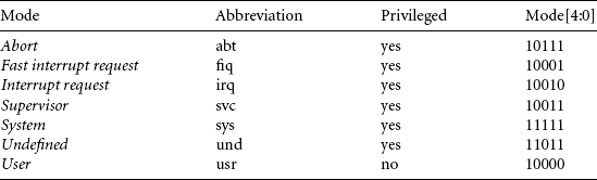
There are seven processor modes in total: six privileged modes (abort, fast interrupt request, interrupt request, supervisor, system, and undefined) and one nonprivileged mode (user).
The processor enters abort mode when there is a failed attempt to access memory. Fast interrupt request and interrupt request modes correspond to the two interrupt levels available on the ARM processor. Supervisor mode is the mode that the processor is in after reset and is generally the mode that an operating system kernel operates in. System mode is a special version of user mode that allows full read-write access to the cpsr. Undefined mode is used when the processor encounters an instruction that is undefined or not supported by the implementation. User mode is used for programs and applications.
2.2.2 BANKED REGISTERS
Figure 2.4 shows all 37 registers in the register file. Of those, 20 registers are hidden from a program at different times. These registers are called banked registers and are identified by the shading in the diagram. They are available only when the processor is in a particular mode; for example, abort mode has banked registers r13_abt, r14_abt and spsr_abt. Banked registers of a particular mode are denoted by an underline character post-fixed to the mode mnemonic or _mode.
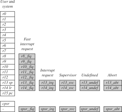
Every processor mode except user mode can change mode by writing directly to the mode bits of the cpsr. All processor modes except system mode have a set of associated banked registers that are a subset of the main 16 registers. A banked register maps one-to-one onto a user mode register. If you change processor mode, a banked register from the new mode will replace an existing register.
For example, when the processor is in the interrupt request mode, the instructions you execute still access registers named r13 and r14. However, these registers are the banked registers r13_irq and r14_irq. The user mode registers r13_usr and r14_usr are not affected by the instruction referencing these registers. A program still has normal access to the other registers r0 to r12.
The processor mode can be changed by a program that writes directly to the cpsr (the processor core has to be in privileged mode) or by hardware when the core responds to an exception or interrupt. The following exceptions and interrupts cause a mode change: reset, interrupt request, fast interrupt request, software interrupt, data abort, prefetch abort, and undefined instruction. Exceptions and interrupts suspend the normal execution of sequential instructions and jump to a specific location.
Figure 2.5 illustrates what happens when an interrupt forces a mode change. The figure shows the core changing from user mode to interrupt request mode, which happens when an interrupt request occurs due to an external device raising an interrupt to the processor core. This change causes user registers r13 and r14 to be banked. The user registers are replaced with registers r13_irq and r14_irq, respectively. Note r14_irq contains the return address and r13_irq contains the stack pointer for interrupt request mode.
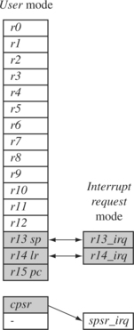
Figure 2.5 also shows a new register appearing in interrupt request mode: the saved program status register (spsr), which stores the previous mode’s cpsr. You can see in the diagram the cpsr being copied into spsr_irq. To return back to user mode, a special return instruction is used that instructs the core to restore the original cpsr from the spsr_irq and bank in the user registers r13 and r14. Note that the spsr can only be modified and read in a privileged mode. There is no spsr available in user mode.
Another important feature to note is that the cpsr is not copied into the spsr when a mode change is forced due to a program writing directly to the cpsr. The saving of the cpsr only occurs when an exception or interrupt is raised.
Figure 2.3 shows that the current active processor mode occupies the five least significant bits of the cpsr. When power is applied to the core, it starts in supervisor mode, which is privileged. Starting in a privileged mode is useful since initialization code can use full access to the cpsr to set up the stacks for each of the other modes.
Table 2.1 lists the various modes and the associated binary patterns. The last column of the table gives the bit patterns that represent each of the processor modes in the cpsr.
2.2.3 STATE AND INSTRUCTION SETS
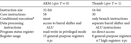
The state of the core determines which instruction set is being executed. There are three instruction sets: ARM, Thumb, and Jazelle. The ARM instruction set is only active when the processor is in ARM state. Similarly the Thumb instruction set is only active when the processor is in Thumb state. Once in Thumb state the processor is executing purely Thumb 16-bit instructions. You cannot intermingle sequential ARM, Thumb, and Jazelle instructions.
The Jazelle J and Thumb T bits in the cpsr reflect the state of the processor. When both J and T bits are 0, the processor is in ARM state and executes ARM instructions. This is the case when power is applied to the processor. When the T bit is 1, then the processor is in Thumb state. To change states the core executes a specialized branch instruction. Table 2.2 compares the ARM and Thumb instruction set features.
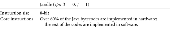
The ARM designers introduced a third instruction set called Jazelle. Jazelle executes 8-bit instructions and is a hybrid mix of software and hardware designed to speed up the execution of Java bytecodes.
To execute Java bytecodes, you require the Jazelle technology plus a specially modified version of the Java virtual machine. It is important to note that the hardware portion of Jazelle only supports a subset of the Java bytecodes; the rest are emulated in software.
The Jazelle instruction set is a closed instruction set and is not openly available. Table 2.3 gives the Jazelle instruction set features.
2.2.4 INTERRUPT MASKS
Interrupt masks are used to stop specific interrupt requests from interrupting the processor. There are two interrupt request levels available on the ARM processor core—interrupt request (IRQ) and fast interrupt request (FIQ).
The cpsr has two interrupt mask bits, 7 and 6 (or I and F), which control the masking of IRQ and FIQ, respectively. The I bit masks IRQ when set to binary 1, and similarly the F bit masks FIQ when set to binary 1.
2.2.5 CONDITION FLAGS
Condition flags are updated by comparisons and the result of ALU operations that specify the S instruction suffix. For example, if a SUBS subtract instruction results in a register value of zero, then the Z flag in the cpsr is set. This particular subtract instruction specifically updates the cpsr.
With processor cores that include the DSP extensions, the Q bit indicates if an overflow or saturation has occurred in an enhanced DSP instruction. The flag is “sticky” in the sense that the hardware only sets this flag. To clear the flag you need to write to the cpsr directly.
In Jazelle-enabled processors, the J bit reflects the state of the core; if it is set, the core is in Jazelle state. The J bit is not generally usable and is only available on some processor cores. To take advantage of Jazelle, extra software has to be licensed from both ARM Limited and Sun Microsystems.
Most ARM instructions can be executed conditionally on the value of the condition flags. Table 2.4 lists the condition flags and a short description on what causes them to be set. These flags are located in the most significant bits in the cpsr. These bits are used for conditional execution.
Table 2.4
| Flag | Flag name | Set when |
| Q | Saturation | the result causes an overflow and/or saturation |
| V | oVerflow | the result causes a signed overflow |
| C | Carry | the result causes an unsigned carry |
| Z | Zero | the result is zero, frequently used to indicate equality |
| N | Negative | bit 31 of the result is a binary 1 |
Figure 2.6 shows a typical value for the cpsr with both DSP extensions and Jazelle. In this book we use a notation that presents the cpsr data in a more human readable form. When a bit is a binary 1 we use a capital letter; when a bit is a binary 0, we use a lowercase letter. For the condition flags a capital letter shows that the flag has been set. For interrupts a capital letter shows that an interrupt is disabled.
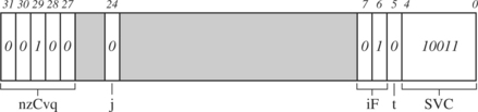
In the cpsr example shown in Figure 2.6, the C flag is the only condition flag set. The rest nzvq flags are all clear. The processor is in ARM state because neither the Jazelle j or Thumb t bits are set. The IRQ interrupts are enabled, and FIQ interrupts are disabled. Finally, you can see from the figure the processor is in supervisor (SVC) mode since the mode[4:0] is equal to binary 10011.
2.2.6 CONDITIONAL EXECUTION
Conditional execution controls whether or not the core will execute an instruction. Most instructions have a condition attribute that determines if the core will execute it based on the setting of the condition flags. Prior to execution, the processor compares the condition attribute with the condition flags in the cpsr. If they match, then the instruction is executed; otherwise the instruction is ignored.
The condition attribute is postfixed to the instruction mnemonic, which is encoded into the instruction. Table 2.5 lists the conditional execution code mnemonics. When a condition mnemonic is not present, the default behavior is to set it to always (AL) execute.
Table 2.5
| Mnemonic | Name | Condition flags |
| EQ | equal | Z |
| NE | not equal | z |
| CS HS | carry set/unsigned higher or same | C |
| CC LO | carry clear/unsigned lower | c |
| MI | minus/negative | N |
| PL | plus/positive or zero | n |
| VS | overflow | V |
| VC | no overflow | v |
| HI | unsigned higher | zC |
| LS | unsigned lower or same | Z or c |
| GE | signed greater than or equal | NV or nv |
| LT | signed less than | Nv or nV |
| GT | signed greater than | NzV or nzv |
| LE | signed less than or equal | Z or Nv or nV |
| AL | always (unconditional) | ignored |
2.3 PIPELINE
A pipeline is the mechanism a RISC processor uses to execute instructions. Using a pipeline speeds up execution by fetching the next instruction while other instructions are being decoded and executed. One way to view the pipeline is to think of it as an automobile assembly line, with each stage carrying out a particular task to manufacture the vehicle.
Figure 2.7 shows a three-stage pipeline:
![]() Fetch loads an instruction from memory.
Fetch loads an instruction from memory.
![]() Decode identifies the instruction to be executed.
Decode identifies the instruction to be executed.
![]() Execute processes the instruction and writes the result back to a register.
Execute processes the instruction and writes the result back to a register.
Figure 2.8 illustrates the pipeline using a simple example. It shows a sequence of three instructions being fetched, decoded, and executed by the processor. Each instruction takes a single cycle to complete after the pipeline is filled.
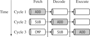
The three instructions are placed into the pipeline sequentially. In the first cycle the core fetches the ADD instruction from memory. In the second cycle the core fetches the SUB instruction and decodes the ADD instruction. In the third cycle, both the SUB and ADD instructions are moved along the pipeline. The ADD instruction is executed, the SUB instruction is decoded, and the CMP instruction is fetched. This procedure is called filling the pipeline. The pipeline allows the core to execute an instruction every cycle.
As the pipeline length increases, the amount of work done at each stage is reduced, which allows the processor to attain a higher operating frequency. This in turn increases the performance. The system latency also increases because it takes more cycles to fill the pipeline before the core can execute an instruction. The increased pipeline length also means there can be data dependency between certain stages. You can write code to reduce this dependency by using instruction scheduling (for more information on instruction scheduling take a look at Chapter 6).
The pipeline design for each ARM family differs. For example, The ARM9 core increases the pipeline length to five stages, as shown in Figure 2.9. The ARM9 adds a memory and writeback stage, which allows the ARM9 to process on average 1.1 Dhrystone MIPS per MHz—an increase in instruction throughput by around 13% compared with an ARM7. The maximum core frequency attainable using an ARM9 is also higher.
The ARM10 increases the pipeline length still further by adding a sixth stage, as shown in Figure 2.10. The ARM10 can process on average 1.3 Dhrystone MIPS per MHz, about 34% more throughput than an ARM7 processor core, but again at a higher latency cost.
Even though the ARM9 and ARM10 pipelines are different, they still use the same pipeline executing characteristics as an ARM7. Code written for the ARM7 will execute on an ARM9 or ARM10.
2.3.1 PIPELINE EXECUTING CHARACTERISTICS
The ARM pipeline has not processed an instruction until it passes completely through the execute stage. For example, an ARM7 pipeline (with three stages) has executed an instruction only when the fourth instruction is fetched.
Figure 2.11 shows an instruction sequence on an ARM7 pipeline. The MSR instruction is used to enable IRQ interrupts, which only occurs once the MSR instruction completes the execute stage of the pipeline. It clears the I bit in the cpsr to enable the IRQ interrupts. Once the ADD instruction enters the execute stage of the pipeline, IRQ interrupts are enabled.
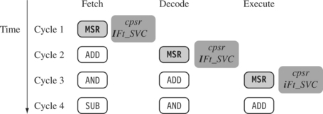
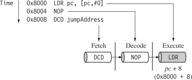
Figure 2.12 illustrates the use of the pipeline and the program counter pc. In the execute stage, the pc always points to the address of the instruction plus 8 bytes. In other words, the pc always points to the address of the instruction being executed plus two instructions ahead. This is important when the pc is used for calculating a relative offset and is an architectural characteristic across all the pipelines. Note when the processor is in Thumb state the pc is the instruction address plus 4.
There are three other characteristics of the pipeline worth mentioning. First, the execution of a branch instruction or branching by the direct modification of the pc causes the ARM core to flush its pipeline.
Second, ARM10 uses branch prediction, which reduces the effect of a pipeline flush by predicting possible branches and loading the new branch address prior to the execution of the instruction.
Third, an instruction in the execute stage will complete even though an interrupt has been raised. Other instructions in the pipeline will be abandoned, and the processor will start filling the pipeline from the appropriate entry in the vector table.
2.4 EXCEPTIONS, INTERRUPTS, AND THE VECTOR TABLE
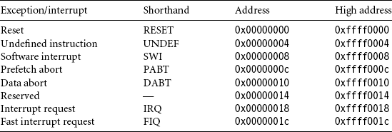
When an exception or interrupt occurs, the processor sets the pc to a specific memory address. The address is within a special address range called the vector table. The entries in the vector table are instructions that branch to specific routines designed to handle a particular exception or interrupt.
The memory map address 0x00000000 is reserved for the vector table, a set of 32-bit words. On some processors the vector table can be optionally located at a higher address in memory (starting at the offset 0xffff0000). Operating systems such as Linux and Microsoft’s embedded products can take advantage of this feature.
When an exception or interrupt occurs, the processor suspends normal execution and starts loading instructions from the exception vector table (see Table 2.6). Each vector table entry contains a form of branch instruction pointing to the start of a specific routine:
![]() Reset vector is the location of the first instruction executed by the processor when power is applied. This instruction branches to the initialization code.
Reset vector is the location of the first instruction executed by the processor when power is applied. This instruction branches to the initialization code.
![]() Undefined instruction vector is used when the processor cannot decode an instruction.
Undefined instruction vector is used when the processor cannot decode an instruction.
![]() Software interrupt vector is called when you execute a SWI instruction. The SWI instruction is frequently used as the mechanism to invoke an operating system routine.
Software interrupt vector is called when you execute a SWI instruction. The SWI instruction is frequently used as the mechanism to invoke an operating system routine.
![]() Prefetch abort vector occurs when the processor attempts to fetch an instruction from an address without the correct access permissions. The actual abort occurs in the decode stage.
Prefetch abort vector occurs when the processor attempts to fetch an instruction from an address without the correct access permissions. The actual abort occurs in the decode stage.
![]() Data abort vector is similar to a prefetch abort but is raised when an instruction attempts to access data memory without the correct access permissions.
Data abort vector is similar to a prefetch abort but is raised when an instruction attempts to access data memory without the correct access permissions.
![]() Interrupt request vector is used by external hardware to interrupt the normal execution flow of the processor. It can only be raised if IRQs are not masked in the cpsr.
Interrupt request vector is used by external hardware to interrupt the normal execution flow of the processor. It can only be raised if IRQs are not masked in the cpsr.
![]() Fast interrupt request vector is similar to the interrupt request but is reserved for hardware requiring faster response times. It can only be raised if FIQs are not masked in the cpsr.
Fast interrupt request vector is similar to the interrupt request but is reserved for hardware requiring faster response times. It can only be raised if FIQs are not masked in the cpsr.
2.5 CORE EXTENSIONS
The hardware extensions covered in this section are standard components placed next to the ARM core. They improve performance, manage resources, and provide extra functionality and are designed to provide flexibility in handling particular applications. Each ARM family has different extensions available.
There are three hardware extensions ARM wraps around the core: cache and tightly coupled memory, memory management, and the coprocessor interface.
2.5.1 CACHE AND TIGHTLY COUPLED MEMORY
The cache is a block of fast memory placed between main memory and the core. It allows for more efficient fetches from some memory types. With a cache the processor core can run for the majority of the time without having to wait for data from slow external memory. Most ARM-based embedded systems use a single-level cache internal to the processor. Of course, many small embedded systems do not require the performance gains that a cache brings.
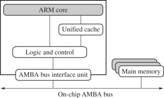
ARM has two forms of cache. The first is found attached to the Von Neumann–style cores. It combines both data and instruction into a single unified cache, as shown in Figure 2.13. For simplicity, we have called the glue logic that connects the memory system to the AMBA bus logic and control.
By contrast, the second form, attached to the Harvard-style cores, has separate caches for data and instruction.
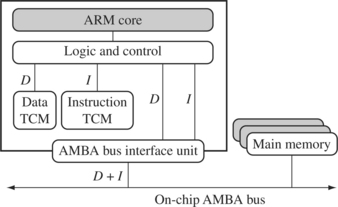
A cache provides an overall increase in performance but at the expense of predictable execution. But for real-time systems it is paramount that code execution is deterministic—the time taken for loading and storing instructions or data must be predictable. This is achieved using a form of memory called tightly coupled memory (TCM). TCM is fast SRAM located close to the core and guarantees the clock cycles required to fetch instructions or data—critical for real-time algorithms requiring deterministic behavior. TCMs appear as memory in the address map and can be accessed as fast memory. An example of a processor with TCMs is shown in Figure 2.14.
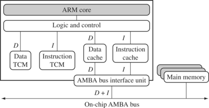
By combining both technologies, ARM processors can have both improved performance and predictable real-time response. Figure 2.15 shows an example core with a combination of caches and TCMs.
2.5.2 MEMORY MANAGEMENT
Embedded systems often use multiple memory devices. It is usually necessary to have a method to help organize these devices and protect the system from applications trying to make inappropriate accesses to hardware. This is achieved with the assistance of memory management hardware.
ARM cores have three different types of memory management hardware—no extensions providing no protection, a memory protection unit (MPU) providing limited protection, and a memory management unit (MMU) providing full protection:
![]() Nonprotected memory is fixed and provides very little flexibility. It is normally used for small, simple embedded systems that require no protection from rogue applications.
Nonprotected memory is fixed and provides very little flexibility. It is normally used for small, simple embedded systems that require no protection from rogue applications.
![]() MPUs employ a simple system that uses a limited number of memory regions. These regions are controlled with a set of special coprocessor registers, and each region is defined with specific access permissions. This type of memory management is used for systems that require memory protection but don’t have a complex memory map. The MPU is explained in Chapter 13.
MPUs employ a simple system that uses a limited number of memory regions. These regions are controlled with a set of special coprocessor registers, and each region is defined with specific access permissions. This type of memory management is used for systems that require memory protection but don’t have a complex memory map. The MPU is explained in Chapter 13.
![]() MMUs are the most comprehensive memory management hardware available on the ARM. The MMU uses a set of translation tables to provide fine-grained control over memory. These tables are stored in main memory and provide a virtual-to-physical address map as well as access permissions. MMUs are designed for more sophisticated platform operating systems that support multitasking. The MMU is explained in Chapter 14.
MMUs are the most comprehensive memory management hardware available on the ARM. The MMU uses a set of translation tables to provide fine-grained control over memory. These tables are stored in main memory and provide a virtual-to-physical address map as well as access permissions. MMUs are designed for more sophisticated platform operating systems that support multitasking. The MMU is explained in Chapter 14.
2.5.3 COPROCESSORS
Coprocessors can be attached to the ARM processor. A coprocessor extends the processing features of a core by extending the instruction set or by providing configuration registers. More than one coprocessor can be added to the ARM core via the coprocessor interface.
The coprocessor can be accessed through a group of dedicated ARM instructions that provide a load-store type interface. Consider, for example, coprocessor 15: The ARM processor uses coprocessor 15 registers to control the cache, TCMs, and memory management.
The coprocessor can also extend the instruction set by providing a specialized group of new instructions. For example, there are a set of specialized instructions that can be added to the standard ARM instruction set to process vector floating-point (VFP) operations.
These new instructions are processed in the decode stage of the ARM pipeline. If the decode stage sees a coprocessor instruction, then it offers it to the relevant coprocessor. But if the coprocessor is not present or doesn’t recognize the instruction, then the ARM takes an undefined instruction exception, which allows you to emulate the behavior of the coprocessor in software.
2.6 ARCHITECTURE REVISIONS
Every ARM processor implementation executes a specific instruction set architecture (ISA), although an ISA revision may have more than one processor implementation.
The ISA has evolved to keep up with the demands of the embedded market. This evolution has been carefully managed by ARM, so that code written to execute on an earlier architecture revision will also execute on a later revision of the architecture.
Before we go on to explain the evolution of the architecture, we must introduce the ARM processor nomenclature. The nomenclature identifies individual processors and provides basic information about the feature set.
2.6.1 NOMENCLATURE
ARM uses the nomenclature shown in Figure 2.16 to describe the processor implementations. The letters and numbers after the word “ARM” indicate the features a processor may have. In the future the number and letter combinations may change as more features are added. Note the nomenclature does not include the architecture revision information.
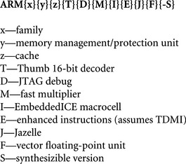
There are a few additional points to make about the ARM nomenclature:
![]() All ARM cores after the ARM7TDMI include the TDMI features even though they may not include those letters after the “ARM” label.
All ARM cores after the ARM7TDMI include the TDMI features even though they may not include those letters after the “ARM” label.
![]() The processor family is a group of processor implementations that share the same hardware characteristics. For example, the ARM7TDMI, ARM740T, and ARM720T all share the same family characteristics and belong to the ARM7 family.
The processor family is a group of processor implementations that share the same hardware characteristics. For example, the ARM7TDMI, ARM740T, and ARM720T all share the same family characteristics and belong to the ARM7 family.
![]() JTAG is described by IEEE 1149.1 Standard Test Access Port and boundary scan architecture. It is a serial protocol used by ARM to send and receive debug information between the processor core and test equipment.
JTAG is described by IEEE 1149.1 Standard Test Access Port and boundary scan architecture. It is a serial protocol used by ARM to send and receive debug information between the processor core and test equipment.
![]() EmbeddedICE macrocell is the debug hardware built into the processor that allows breakpoints and watchpoints to be set.
EmbeddedICE macrocell is the debug hardware built into the processor that allows breakpoints and watchpoints to be set.
![]() Synthesizable means that the processor core is supplied as source code that can be compiled into a form easily used by EDA tools.
Synthesizable means that the processor core is supplied as source code that can be compiled into a form easily used by EDA tools.
2.6.2 ARCHITECTURE EVOLUTION
The architecture has continued to evolve since the first ARM processor implementation was introduced in 1985. Table 2.7 shows the significant architecture enhancements from the original architecture version 1 to the current version 6 architecture. One of the most significant changes to the ISA was the introduction of the Thumb instruction set in ARMv4T (the ARM7TDMI processor).
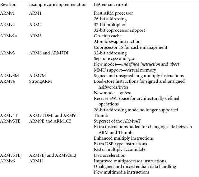
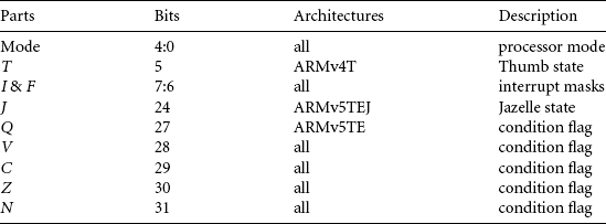
Table 2.8 summarizes the various parts of the program status register and the availability of certain features on particular instruction architectures. “All” refers to the ARMv4 architecture and above.
2.7 ARM PROCESSOR FAMILIES
ARM has designed a number of processors that are grouped into different families according to the core they use. The families are based on the ARM7, ARM9, ARM10, and ARM11 cores. The postfix numbers 7, 9, 10, and 11 indicate different core designs. The ascending number equates to an increase in performance and sophistication. ARM8 was developed but was soon superseded.
Table 2.9 shows a rough comparison of attributes between the ARM7, ARM9, ARM10, and ARM11 cores. The numbers quoted can vary greatly and are directly dependent upon the type and geometry of the manufacturing process, which has a direct effect on the frequency (MHz) and power consumption (watts).
Table 2.9
ARM family attribute comparison.
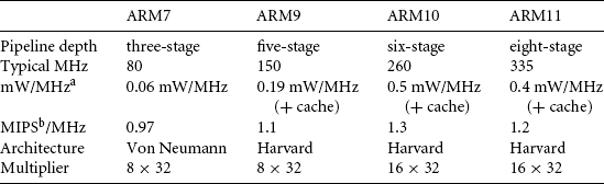
aWatts/MHz on the same 0.13 micron process.
bMIPS are Dhrystone VAX MIPS.
Within each ARM family, there are a number of variations of memory management, cache, and TCM processor extensions. ARM continues to expand both the number of families available and the different variations within each family.
You can find other processors that execute the ARM ISA such as StrongARM and XScale. These processors are unique to a particular semiconductor company, in this case Intel.
Table 2.10 summarizes the different features of the various processors. The next subsections describe the ARM families in more detail, starting with the ARM7 family.
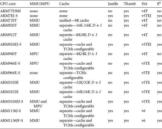
2.7.1 ARM7 FAMILY
The ARM7 core has a Von Neumann–style architecture, where both data and instructions use the same bus. The core has a three-stage pipeline and executes the architecture ARMv4T instruction set.
The ARM7TDMI was the first of a new range of processors introduced in 1995 by ARM. It is currently a very popular core and is used in many 32-bit embedded processors. It provides a very good performance-to-power ratio. The ARM7TDMI processor core has been licensed by many of the top semiconductor companies around the world and is the first core to include the Thumb instruction set, a fast multiply instruction, and the EmbeddedICE debug technology.
One significant variation in the ARM7 family is the ARM7TDMI-S. The ARM7TDMI-S has the same operating characteristics as a standard ARM7TDMI but is also synthesizable.
ARM720T is the most flexible member of the ARM7 family because it includes an MMU. The presence of the MMU means the ARM720T is capable of handling the Linux and Microsoft embedded platform operating systems. The processor also includes a unified 8K cache. The vector table can be relocated to a higher address by setting a coprocessor 15 register.
Another variation is the ARM7EJ-S processor, also synthesizable. ARM7EJ-S is quite different since it includes a five-stage pipeline and executes ARMv5TEJ instructions. This version of the ARM7 is the only one that provides both Java acceleration and the enhanced instructions but without any memory protection.
2.7.2 ARM9 FAMILY
The ARM9 family was announced in 1997. Because of its five-stage pipeline, the ARM9 processor can run at higher clock frequencies than the ARM7 family. The extra stages improve the overall performance of the processor. The memory system has been redesigned to follow the Harvard architecture, which separates the data D and instruction I buses.
The first processor in the ARM9 family was the ARM920T, which includes a separate D + I cache and an MMU. This processor can be used by operating systems requiring virtual memory support. ARM922T is a variation on the ARM920T but with half the D + I cache size.
The ARM940T includes a smaller D + I cache and an MPU. The ARM940T is designed for applications that do not require a platform operating system. Both ARM920T and ARM940T execute the architecture v4T instructions.
The next processors in the ARM9 family were based on the ARM9E-S core. This core is a synthesizable version of the ARM9 core with the E extensions. There are two variations: the ARM946E-S and the ARM966E-S. Both execute architecture v5TE instructions. They also support the optional embedded trace macrocell (ETM), which allows a developer to trace instruction and data execution in real time on the processor. This is important when debugging applications with time-critical segments.
The ARM946E-S includes TCM, cache, and an MPU. The sizes of the TCM and caches are configurable. This processor is designed for use in embedded control applications that require deterministic real-time response. In contrast, the ARM966E does not have the MPU and cache extensions but does have configurable TCMs.
The latest core in the ARM9 product line is the ARM926EJ-S synthesizable processor core, announced in 2000. It is designed for use in small portable Java-enabled devices such as 3G phones and personal digital assistants (PDAs). The ARM926EJ-S is the first ARM processor core to include the Jazelle technology, which accelerates Java bytecode execution. It features an MMU, configurable TCMs, and D + I caches with zero or nonzero wait state memories.
2.7.3 ARM10 FAMILY
The ARM10, announced in 1999, was designed for performance. It extends the ARM9 pipeline to six stages. It also supports an optional vector floating-point (VFP) unit, which adds a seventh stage to the ARM10 pipeline. The VFP significantly increases floating-point performance and is compliant with the IEEE 754.1985 floating-point standard.
The ARM1020E is the first processor to use an ARM10E core. Like the ARM9E, it includes the enhanced E instructions. It has separate 32K D + I caches, optional vector floating-point unit, and an MMU. The ARM1020E also has a dual 64-bit bus interface for increased performance.
ARM1026EJ-S is very similar to the ARM926EJ-S but with both MPU and MMU. This processor has the performance of the ARM10 with the flexibility of an ARM926EJ-S.
2.7.4 ARM11 FAMILY
The ARM1136J-S, announced in 2003, was designed for high performance and power-efficient applications. ARM1136J-S was the first processor implementation to execute architecture ARMv6 instructions. It incorporates an eight-stage pipeline with separate load-store and arithmetic pipelines. Included in the ARMv6 instructions are single instruction multiple data (SIMD) extensions for media processing, specifically designed to increase video processing performance.
The ARM1136JF-S is an ARM1136J-S with the addition of the vector floating-point unit for fast floating-point operations.
2.7.5 SPECIALIZED PROCESSORS
StrongARM was originally co-developed by Digital Semiconductor and is now exclusively licensed by Intel Corporation. It is has been popular for PDAs and applications that require performance with low power consumption. It is a Harvard architecture with separate D + I caches. StrongARM was the first high-performance ARM processor to include a five-stage pipeline, but it does not support the Thumb instruction set.
Intel’s XScale is a follow-on product to the StrongARM and offers dramatic increases in performance. At the time of writing, XScale was quoted as being able to run up to 1 GHz. XScale executes architecture v5TE instructions. It is a Harvard architecture and is similar to the StrongARM, as it also includes an MMU.
SC100 is at the other end of the performance spectrum. It is designed specifically for low-power security applications. The SC100 is the first SecurCore and is based on an ARM7TDMI core with an MPU. This core is small and has low voltage and current requirements, which makes it attractive for smart card applications.
2.8 SUMMARY
In this chapter we focused on the hardware fundamentals of the actual ARM processor. The ARM processor can be abstracted into eight components—ALU, barrel shifter, MAC, register file, instruction decoder, address register, incrementer, and sign extend.
ARM has three instruction sets—ARM, Thumb, and Jazelle. The register file contains 37 registers, but only 17 or 18 registers are accessible at any point in time; the rest are banked according to processor mode. The current processor mode is stored in the cpsr. It holds the current status of the processor core as well interrupt masks, condition flags, and state. The state determines which instruction set is being executed.
An ARM processor comprises a core plus the surrounding components that interface it with a bus. The core extensions include the following:
![]() Caches are used to improve the overall system performance.
Caches are used to improve the overall system performance.
![]() TCMs are used to improve deterministic real-time response.
TCMs are used to improve deterministic real-time response.
![]() Memory management is used to organize memory and protect system resources.
Memory management is used to organize memory and protect system resources.
![]() Coprocessors are used to extend the instruction set and functionality. Coprocessor 15 controls the cache, TCMs, and memory management.
Coprocessors are used to extend the instruction set and functionality. Coprocessor 15 controls the cache, TCMs, and memory management.
An ARM processor is an implementation of a specific instruction set architecture (ISA). The ISA has been continuously improved from the first ARM processor design. Processors are grouped into implementation families (ARM7, ARM9, ARM10, and ARM11) with similar characteristics.