
ARM EMBEDDED SYSTEMS
The ARM processor core is a key component of many successful 32-bit embedded systems. You probably own one yourself and may not even realize it! ARM cores are widely used in mobile phones, handheld organizers, and a multitude of other everyday portable consumer devices.
ARM’s designers have come a long way from the first ARM1 prototype in 1985. Over one billion ARM processors had been shipped worldwide by the end of 2001. The ARM company bases their success on a simple and powerful original design, which continues to improve today through constant technical innovation. In fact, the ARM core is not a single core, but a whole family of designs sharing similar design principles and a common instruction set.
For example, one of ARM’s most successful cores is the ARM7TDMI. It provides up to 120 Dhrystone MIPS1 and is known for its high code density and low power consumption, making it ideal for mobile embedded devices.
In this first chapter we discuss how the RISC (reduced instruction set computer) design philosophy was adapted by ARM to create a flexible embedded processor. We then introduce an example embedded device and discuss the typical hardware and software technologies that surround an ARM processor.
1.1 THE RISC DESIGN PHILOSOPHY
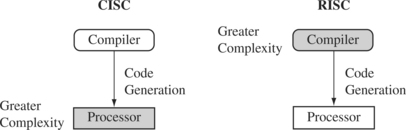
The ARM core uses a RISC architecture. RISC is a design philosophy aimed at delivering simple but powerful instructions that execute within a single cycle at a high clock speed. The RISC philosophy concentrates on reducing the complexity of instructions performed by the hardware because it is easier to provide greater flexibility and intelligence in software rather than hardware. As a result, a RISC design places greater demands on the compiler. In contrast, the traditional complex instruction set computer (CISC) relies more on the hardware for instruction functionality, and consequently the CISC instructions are more complicated. Figure 1.1 illustrates these major differences.
The RISC philosophy is implemented with four major design rules:
1. Instructions—RISC processors have a reduced number of instruction classes. These classes provide simple operations that can each execute in a single cycle. The compiler or programmer synthesizes complicated operations (for example, a divide operation) by combining several simple instructions. Each instruction is a fixed length to allow the pipeline to fetch future instructions before decoding the current instruction. In contrast, in CISC processors the instructions are often of variable size and take many cycles to execute.
2. Pipelines—The processing of instructions is broken down into smaller units that can be executed in parallel by pipelines. Ideally the pipeline advances by one step on each cycle for maximum throughput. Instructions can be decoded in one pipeline stage. There is no need for an instruction to be executed by a miniprogram called microcode as on CISC processors.
3. Registers—RISC machines have a large general-purpose register set. Any register can contain either data or an address. Registers act as the fast local memory store for all data processing operations. In contrast, CISC processors have dedicated registers for specific purposes.
4. Load-store architecture—The processor operates on data held in registers. Separate load and store instructions transfer data between the register bank and external memory. Memory accesses are costly, so separating memory accesses from data processing provides an advantage because you can use data items held in the register bank multiple times without needing multiple memory accesses. In contrast, with a CISC design the data processing operations can act on memory directly.
These design rules allow a RISC processor to be simpler, and thus the core can operate at higher clock frequencies. In contrast, traditional CISC processors are more complex and operate at lower clock frequencies. Over the course of two decades, however, the distinction between RISC and CISC has blurred as CISC processors have implemented more RISC concepts.
1.2 THE ARM DESIGN PHILOSOPHY
There are a number of physical features that have driven the ARM processor design. First, portable embedded systems require some form of battery power. The ARM processor has been specifically designed to be small to reduce power consumption and extend battery operation—essential for applications such as mobile phones and personal digital assistants (PDAs).
High code density is another major requirement since embedded systems have limited memory due to cost and/or physical size restrictions. High code density is useful for applications that have limited on-board memory, such as mobile phones and mass storage devices.
In addition, embedded systems are price sensitive and use slow and low-cost memory devices. For high-volume applications like digital cameras, every cent has to be accounted for in the design. The ability to use low-cost memory devices produces substantial savings.
Another important requirement is to reduce the area of the die taken up by the embedded processor. For a single-chip solution, the smaller the area used by the embedded processor, the more available space for specialized peripherals. This in turn reduces the cost of the design and manufacturing since fewer discrete chips are required for the end product.
ARM has incorporated hardware debug technology within the processor so that software engineers can view what is happening while the processor is executing code. With greater visibility, software engineers can resolve issues faster, which has a direct effect on the time to market and reduces overall development costs.
The ARM core is not a pure RISC architecture because of the constraints of its primary application—the embedded system. In some sense, the strength of the ARM core is that it does not take the RISC concept too far. In today’s systems the key is not raw processor speed but total effective system performance and power consumption.
1.2.1 INSTRUCTION SET FOR EMBEDDED SYSTEMS
The ARM instruction set differs from the pure RISC definition in several ways that make the ARM instruction set suitable for embedded applications:
![]() Variable cycle execution for certain instructions—Not every ARM instruction executes in a single cycle. For example, load-store-multiple instructions vary in the number of execution cycles depending upon the number of registers being transferred. The transfer can occur on sequential memory addresses, which increases performance since sequential memory accesses are often faster than random accesses. Code density is also improved since multiple register transfers are common operations at the start and end of functions.
Variable cycle execution for certain instructions—Not every ARM instruction executes in a single cycle. For example, load-store-multiple instructions vary in the number of execution cycles depending upon the number of registers being transferred. The transfer can occur on sequential memory addresses, which increases performance since sequential memory accesses are often faster than random accesses. Code density is also improved since multiple register transfers are common operations at the start and end of functions.
![]() Inline barrel shifter leading to more complex instructions—The inline barrel shifter is a hardware component that preprocesses one of the input registers before it is used by an instruction. This expands the capability of many instructions to improve core performance and code density. We explain this feature in more detail in Chapters 2, 3, and 4.
Inline barrel shifter leading to more complex instructions—The inline barrel shifter is a hardware component that preprocesses one of the input registers before it is used by an instruction. This expands the capability of many instructions to improve core performance and code density. We explain this feature in more detail in Chapters 2, 3, and 4.
![]() Thumb 16-bit instruction set—ARM enhanced the processor core by adding a second 16-bit instruction set called Thumb that permits the ARM core to execute either 16- or 32-bit instructions. The 16-bit instructions improve code density by about 30% over 32-bit fixed-length instructions.
Thumb 16-bit instruction set—ARM enhanced the processor core by adding a second 16-bit instruction set called Thumb that permits the ARM core to execute either 16- or 32-bit instructions. The 16-bit instructions improve code density by about 30% over 32-bit fixed-length instructions.
![]() Conditional execution—An instruction is only executed when a specific condition has been satisfied. This feature improves performance and code density by reducing branch instructions.
Conditional execution—An instruction is only executed when a specific condition has been satisfied. This feature improves performance and code density by reducing branch instructions.
![]() Enhanced instructions—The enhanced digital signal processor (DSP) instructions were added to the standard ARM instruction set to support fast 16 × 16-bit multiplier operations and saturation. These instructions allow a faster-performing ARM processor in some cases to replace the traditional combinations of a processor plus a DSP.
Enhanced instructions—The enhanced digital signal processor (DSP) instructions were added to the standard ARM instruction set to support fast 16 × 16-bit multiplier operations and saturation. These instructions allow a faster-performing ARM processor in some cases to replace the traditional combinations of a processor plus a DSP.
These additional features have made the ARM processor one of the most commonly used 32-bit embedded processor cores. Many of the top semiconductor companies around the world produce products based around the ARM processor.
1.3 EMBEDDED SYSTEM HARDWARE
Embedded systems can control many different devices, from small sensors found on a production line, to the real-time control systems used on a NASA space probe. All these devices use a combination of software and hardware components. Each component is chosen for efficiency and, if applicable, is designed for future extension and expansion.
Figure 1.2 shows a typical embedded device based on an ARM core. Each box represents a feature or function. The lines connecting the boxes are the buses carrying data. We can separate the device into four main hardware components:
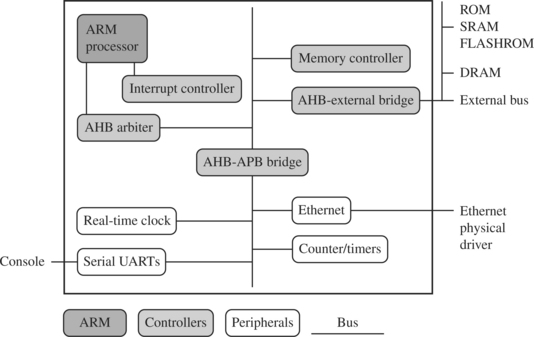
![]() The ARM processor controls the embedded device. Different versions of the ARM processor are available to suit the desired operating characteristics. An ARM processor comprises a core (the execution engine that processes instructions and manipulates data) plus the surrounding components that interface it with a bus. These components can include memory management and caches.
The ARM processor controls the embedded device. Different versions of the ARM processor are available to suit the desired operating characteristics. An ARM processor comprises a core (the execution engine that processes instructions and manipulates data) plus the surrounding components that interface it with a bus. These components can include memory management and caches.
![]() Controllers coordinate important functional blocks of the system. Two commonly found controllers are interrupt and memory controllers.
Controllers coordinate important functional blocks of the system. Two commonly found controllers are interrupt and memory controllers.
![]() The peripherals provide all the input-output capability external to the chip and are responsible for the uniqueness of the embedded device.
The peripherals provide all the input-output capability external to the chip and are responsible for the uniqueness of the embedded device.
![]() A bus is used to communicate between different parts of the device.
A bus is used to communicate between different parts of the device.
1.3.1 ARM BUS TECHNOLOGY
Embedded systems use different bus technologies than those designed for x86 PCs. The most common PC bus technology, the Peripheral Component Interconnect (PCI) bus, connects such devices as video cards and hard disk controllers to the x86 processor bus. This type of technology is external or off-chip (i.e., the bus is designed to connect mechanically and electrically to devices external to the chip) and is built into the motherboard of a PC.
In contrast, embedded devices use an on-chip bus that is internal to the chip and that allows different peripheral devices to be interconnected with an ARM core.
There are two different classes of devices attached to the bus. The ARM processor core is a bus master—a logical device capable of initiating a data transfer with another device across the same bus. Peripherals tend to be bus slaves—logical devices capable only of responding to a transfer request from a bus master device.
A bus has two architecture levels. The first is a physical level that covers the electrical characteristics and bus width (16, 32, or 64 bits). The second level deals with protocol—the logical rules that govern the communication between the processor and a peripheral.
ARM is primarily a design company. It seldom implements the electrical characteristics of the bus, but it routinely specifies the bus protocol.
1.3.2 AMBA BUS PROTOCOL
The Advanced Microcontroller Bus Architecture (AMBA) was introduced in 1996 and has been widely adopted as the on-chip bus architecture used for ARM processors. The first AMBA buses introduced were the ARM System Bus (ASB) and the ARM Peripheral Bus (APB). Later ARM introduced another bus design, called the ARM High Performance Bus (AHB). Using AMBA, peripheral designers can reuse the same design on multiple projects. Because there are a large number of peripherals developed with an AMBA interface, hardware designers have a wide choice of tested and proven peripherals for use in a device. A peripheral can simply be bolted onto the on-chip bus without having to redesign an interface for each different processor architecture. This plug-and-play interface for hardware developers improves availability and time to market.
AHB provides higher data throughput than ASB because it is based on a centralized multiplexed bus scheme rather than the ASB bidirectional bus design. This change allows the AHB bus to run at higher clock speeds and to be the first ARM bus to support widths of 64 and 128 bits. ARM has introduced two variations on the AHB bus: Multi-layer AHB and AHB-Lite. In contrast to the original AHB, which allows a single bus master to be active on the bus at any time, the Multi-layer AHB bus allows multiple active bus masters. AHB-Lite is a subset of the AHB bus and it is limited to a single bus master. This bus was developed for designs that do not require the full features of the standard AHB bus.
AHB and Multi-layer AHB support the same protocol for master and slave but have different interconnects. The new interconnects in Multi-layer AHB are good for systems with multiple processors. They permit operations to occur in parallel and allow for higher throughput rates.
The example device shown in Figure 1.2 has three buses: an AHB bus for the high-performance peripherals, an APB bus for the slower peripherals, and a third bus for external peripherals, proprietary to this device. This external bus requires a specialized bridge to connect with the AHB bus.
1.3.3 MEMORY
An embedded system has to have some form of memory to store and execute code. You have to compare price, performance, and power consumption when deciding upon specific memory characteristics, such as hierarchy, width, and type. If memory has to run twice as fast to maintain a desired bandwidth, then the memory power requirement may be higher.
1.3.3.1 Hierarchy
All computer systems have memory arranged in some form of hierarchy. Figure 1.2 shows a device that supports external off-chip memory. Internal to the processor there is an option of a cache (not shown in Figure 1.2) to improve memory performance.
Figure 1.3 shows the memory trade-offs: the fastest memory cache is physically located nearer the ARM processor core and the slowest secondary memory is set further away. Generally the closer memory is to the processor core, the more it costs and the smaller its capacity.
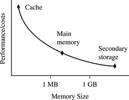
The cache is placed between main memory and the core. It is used to speed up data transfer between the processor and main memory. A cache provides an overall increase in performance but with a loss of predictable execution time. Although the cache increases the general performance of the system, it does not help real-time system response. Note that many small embedded systems do not require the performance benefits of a cache.
The main memory is large—around 256 KB to 256 MB (or even greater), depending on the application—and is generally stored in separate chips. Load and store instructions access the main memory unless the values have been stored in the cache for fast access. Secondary storage is the largest and slowest form of memory. Hard disk drives and CD-ROM drives are examples of secondary storage. These days secondary storage may vary from 600 MB to 60 GB.
1.3.3.2 Width
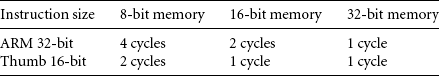
The memory width is the number of bits the memory returns on each access—typically 8, 16, 32, or 64 bits. The memory width has a direct effect on the overall performance and cost ratio.
If you have an uncached system using 32-bit ARM instructions and 16-bit-wide memory chips, then the processor will have to make two memory fetches per instruction. Each fetch requires two 16-bit loads. This obviously has the effect of reducing system performance, but the benefit is that 16-bit memory is less expensive.
In contrast, if the core executes 16-bit Thumb instructions, it will achieve better performance with a 16-bit memory. The higher performance is a result of the core making only a single fetch to memory to load an instruction. Hence, using Thumb instructions with 16-bit-wide memory devices provides both improved performance and reduced cost.
Table 1.1 summarizes theoretical cycle times on an ARM processor using different memory width devices.
1.3.3.3 Types
There are many different types of memory. In this section we describe some of the more popular memory devices found in ARM-based embedded systems.
Read-only memory (ROM) is the least flexible of all memory types because it contains an image that is permanently set at production time and cannot be reprogrammed. ROMs are used in high-volume devices that require no updates or corrections. Many devices also use a ROM to hold boot code.
Flash ROM can be written to as well as read, but it is slow to write so you shouldn’t use it for holding dynamic data. Its main use is for holding the device firmware or storing long-term data that needs to be preserved after power is off. The erasing and writing of flash ROM are completely software controlled with no additional hardware circuity required, which reduces the manufacturing costs. Flash ROM has become the most popular of the read-only memory types and is currently being used as an alternative for mass or secondary storage.
Dynamic random access memory (DRAM) is the most commonly used RAM for devices. It has the lowest cost per megabyte compared with other types of RAM. DRAM is dynamic—it needs to have its storage cells refreshed and given a new electronic charge every few milliseconds, so you need to set up a DRAM controller before using the memory.
Static random access memory (SRAM) is faster than the more traditional DRAM, but requires more silicon area. SRAM is static—the RAM does not require refreshing. The access time for SRAM is considerably shorter than the equivalent DRAM because SRAM does not require a pause between data accesses. Because of its higher cost, it is used mostly for smaller high-speed tasks, such as fast memory and caches.
Synchronous dynamic random access memory (SDRAM) is one of many subcategories of DRAM. It can run at much higher clock speeds than conventional memory. SDRAM synchronizes itself with the processor bus because it is clocked. Internally the data is fetched from memory cells, pipelined, and finally brought out on the bus in a burst. The old-style DRAM is asynchronous, so does not burst as efficiently as SDRAM.
1.3.4 PERIPHERALS
Embedded systems that interact with the outside world need some form of peripheral device. A peripheral device performs input and output functions for the chip by connecting to other devices or sensors that are off-chip. Each peripheral device usually performs a single function and may reside on-chip. Peripherals range from a simple serial communication device to a more complex 802.11 wireless device.
All ARM peripherals are memory mapped—the programming interface is a set of memory-addressed registers. The address of these registers is an offset from a specific peripheral base address.
Controllers are specialized peripherals that implement higher levels of functionality within an embedded system. Two important types of controllers are memory controllers and interrupt controllers.
1.3.4.1 Memory Controllers
Memory controllers connect different types of memory to the processor bus. On power-up a memory controller is configured in hardware to allow certain memory devices to be active. These memory devices allow the initialization code to be executed. Some memory devices must be set up by software; for example, when using DRAM, you first have to set up the memory timings and refresh rate before it can be accessed.
1.3.4.2 Interrupt Controllers
When a peripheral or device requires attention, it raises an interrupt to the processor. An interrupt controller provides a programmable governing policy that allows software to determine which peripheral or device can interrupt the processor at any specific time by setting the appropriate bits in the interrupt controller registers.
There are two types of interrupt controller available for the ARM processor: the standard interrupt controller and the vector interrupt controller (VIC).
The standard interrupt controller sends an interrupt signal to the processor core when an external device requests servicing. It can be programmed to ignore or mask an individual device or set of devices. The interrupt handler determines which device requires servicing by reading a device bitmap register in the interrupt controller.
The VIC is more powerful than the standard interrupt controller because it prioritizes interrupts and simplifies the determination of which device caused the interrupt. After associating a priority and a handler address with each interrupt, the VIC only asserts an interrupt signal to the core if the priority of a new interrupt is higher than the currently executing interrupt handler. Depending on its type, the VIC will either call the standard interrupt exception handler, which can load the address of the handler for the device from the VIC, or cause the core to jump to the handler for the device directly.
1.4 EMBEDDED SYSTEM SOFTWARE
An embedded system needs software to drive it. Figure 1.4 shows four typical software components required to control an embedded device. Each software component in the stack uses a higher level of abstraction to separate the code from the hardware device.
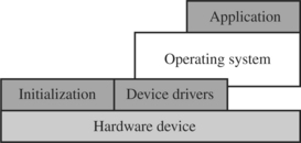
The initialization code is the first code executed on the board and is specific to a particular target or group of targets. It sets up the minimum parts of the board before handing control over to the operating system.
The operating system provides an infrastructure to control applications and manage hardware system resources. Many embedded systems do not require a full operating system but merely a simple task scheduler that is either event or poll driven.
The device drivers are the third component shown in Figure 1.4. They provide a consistent software interface to the peripherals on the hardware device.
Finally, an application performs one of the tasks required for a device. For example, a mobile phone might have a diary application. There may be multiple applications running on the same device, controlled by the operating system.
The software components can run from ROM or RAM. ROM code that is fixed on the device (for example, the initialization code) is called firmware.
1.4.1 INITIALIZATION (BOOT) CODE
Initialization code (or boot code) takes the processor from the reset state to a state where the operating system can run. It usually configures the memory controller and processor caches and initializes some devices. In a simple system the operating system might be replaced by a simple scheduler or debug monitor.
The initialization code handles a number of administrative tasks prior to handing control over to an operating system image. We can group these different tasks into three phases: initial hardware configuration, diagnostics, and booting.
Initial hardware configuration involves setting up the target platform so it can boot an image. Although the target platform itself comes up in a standard configuration, this configuration normally requires modification to satisfy the requirements of the booted image. For example, the memory system normally requires reorganization of the memory map, as shown in Example 1.1.
Diagnostics are often embedded in the initialization code. Diagnostic code tests the system by exercising the hardware target to check if the target is in working order. It also tracks down standard system-related issues. This type of testing is important for manufacturing since it occurs after the software product is complete. The primary purpose of diagnostic code is fault identification and isolation.
Booting involves loading an image and handing control over to that image. The boot process itself can be complicated if the system must boot different operating systems or different versions of the same operating system.
Booting an image is the final phase, but first you must load the image. Loading an image involves anything from copying an entire program including code and data into RAM, to just copying a data area containing volatile variables into RAM. Once booted, the system hands over control by modifying the program counter to point into the start of the image.
Sometimes, to reduce the image size, an image is compressed. The image is then decompressed either when it is loaded or when control is handed over to it.
EXAMPLE 1.1
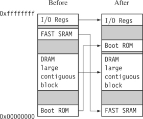
Initializing or organizing memory is an important part of the initialization code because many operating systems expect a known memory layout before they can start.
Figure 1.5 shows memory before and after reorganization. It is common for ARM-based embedded systems to provide for memory remapping because it allows the system to start the initialization code from ROM at power-up. The initialization code then redefines or remaps the memory map to place RAM at address 0x00000000—an important step because then the exception vector table can be in RAM and thus can be reprogrammed. We will discuss the vector table in more detail in Section 2.4.
1.4.2 OPERATING SYSTEM
The initialization process prepares the hardware for an operating system to take control. An operating system organizes the system resources: the peripherals, memory, and processing time. With an operating system controlling these resources, they can be efficiently used by different applications running within the operating system environment.
ARM processors support over 50 operating systems. We can divide operating systems into two main categories: real-time operating systems (RTOSs) and platform operating systems.
RTOSs provide guaranteed response times to events. Different operating systems have different amounts of control over the system response time. A hard real-time application requires a guaranteed response to work at all. In contrast, a soft real-time application requires a good response time, but the performance degrades more gracefully if the response time overruns. Systems running an RTOS generally do not have secondary storage.
Platform operating systems require a memory management unit to manage large, non-real-time applications and tend to have secondary storage. The Linux operating system is a typical example of a platform operating system.
These two categories of operating system are not mutually exclusive: there are operating systems that use an ARM core with a memory management unit and have real-time characteristics. ARM has developed a set of processor cores that specifically target each category.
1.4.3 APPLICATIONS
The operating system schedules applications—code dedicated to handling a particular task. An application implements a processing task; the operating system controls the environment. An embedded system can have one active application or several applications running simultaneously.
ARM processors are found in numerous market segments, including networking, automotive, mobile and consumer devices, mass storage, and imaging. Within each segment ARM processors can be found in multiple applications.
For example, the ARM processor is found in networking applications like home gateways, DSL modems for high-speed Internet communication, and 802.11 wireless communication. The mobile device segment is the largest application area for ARM processors because of mobile phones. ARM processors are also found in mass storage devices such as hard drives and imaging products such as inkjet printers—applications that are cost sensitive and high volume.
In contrast, ARM processors are not found in applications that require leading-edge high performance. Because these applications tend to be low volume and high cost, ARM has decided not to focus designs on these types of applications.
1.5 SUMMARY
Pure RISC is aimed at high performance, but ARM uses a modified RISC design philosophy that also targets good code density and low power consumption. An embedded system consists of a processor core surrounded by caches, memory, and peripherals. The system is controlled by operating system software that manages application tasks.
The key points in a RISC design philosophy are to improve performance by reducing the complexity of instructions, to speed up instruction processing by using a pipeline, to provide a large register set to store data near the core, and to use a load-store architecture.
The ARM design philosophy also incorporates some non-RISC ideas:
![]() It allows variable cycle execution on certain instructions to save power, area, and code size.
It allows variable cycle execution on certain instructions to save power, area, and code size.
![]() It adds a barrel shifter to expand the capability of certain instructions.
It adds a barrel shifter to expand the capability of certain instructions.
![]() It uses the Thumb 16-bit instruction set to improve code density.
It uses the Thumb 16-bit instruction set to improve code density.
![]() It improves code density and performance by conditionally executing instructions.
It improves code density and performance by conditionally executing instructions.
![]() It includes enhanced instructions to perform digital signal processing type functions.
It includes enhanced instructions to perform digital signal processing type functions.
An embedded system includes the following hardware components: ARM processors are found embedded in chips. Programmers access peripherals through memory-mapped registers. There is a special type of peripheral called a controller, which embedded systems use to configure higher-level functions such as memory and interrupts. The AMBA on-chip bus is used to connect the processor and peripherals together.
An embedded system also includes the following software components: Initialization code configures the hardware to a known state. Once configured, operating systems can be loaded and executed. Operating systems provide a common programming environment for the use of hardware resources and infrastructure. Device drivers provide a standard interface to peripherals. An application performs the task-specific duties of an embedded system.
1Dhrystone MIPS version 2.1 is a small benchmarking program.