
INTRODUCTION TO THE ARM INSTRUCTION SET
3.1. DATA PROCESSING INSTRUCTIONS
3.1.3. Arithmetic Instructions
3.1.4. Using the Barrel Shifter with Arithmetic Instructions
3.3.1. Single-Register Transfer
3.3.2. Single-Register Load-Store Addressing Modes
3.4. SOFTWARE INTERRUPT INSTRUCTION
This introduction to the ARM instruction set is a fundamental chapter since the information presented here is used throughout the rest of the book. Consequently, it is placed here before we start going into any depth on optimization and efficient algorithms. This chapter introduces the most common and useful ARM instructions and builds on the ARM processor fundamentals covered in the last chapter. Chapter 4 introduces the Thumb instruction set, and Appendix A gives a complete description of all ARM instructions.
Different ARM architecture revisions support different instructions. However, new revisions usually add instructions and remain backwardly compatible. Code you write for architecture ARMv4T should execute on an ARMv5TE processor. Table 3.1 provides a complete list of ARM instructions available in the ARMv5E instruction set architecture (ISA). This ISA includes all the core ARM instructions as well as some of the newer features in the ARM instruction set. The “ARM ISA” column lists the ISA revision in which the instruction was introduced. Some instructions have extended functionality in later architectures; for example, the CDP instruction has an ARMv5 variant called CDP2. Similarly, instructions such as LDR have ARMv5 additions but do not require a new or extended mnemonic.
Table 3.1
| Mnemonics | ARM ISA | Description |
| ADC | v1 | add two 32-bit values and carry |
| ADD | v1 | add two 32-bit values |
| AND | v1 | logical bitwise AND of two 32-bit values |
| B | v1 | branch relative +/− 32 MB |
| BIC | v1 | logical bit clear (AND NOT) of two 32-bit values |
| BKPT | v5 | breakpoint instructions |
| BL | v1 | relative branch with link |
| BLX | v5 | branch with link and exchange |
| BX | v4T | branch with exchange |
| CDP CDP2 | v2 v5 | coprocessor data processing operation |
| CLZ | v5 | count leading zeros |
| CMN | v1 | compare negative two 32-bit values |
| CMP | v1 | compare two 32-bit values |
| EOR | v1 | logical exclusive OR of two 32-bit values |
| LDC LDC2 | v2 v5 | load to coprocessor single or multiple 32-bit values |
| LDM | v1 | load multiple 32-bit words from memory to ARM registers |
| LDR | v1 v4 v5E | load a single value from a virtual address in memory |
| MCR MCR2 MCRR | v2 v5 v5E | move to coprocessor from an ARM register or registers |
| MLA | v2 | multiply and accumulate 32-bit values |
| MOV | v1 | move a 32-bit value into a register |
| MRC MRC2 MRRC | v2 v5 v5E | move to ARM register or registers from a coprocessor |
| MRS | v3 | move to ARM register from a status register (cpsr or spsr) |
| MSR | v3 | move to a status register (cpsr or spsr) from an ARM register |
| MUL | v2 | multiply two 32-bit values |
| MVN | v1 | move the logical NOT of 32-bit value into a register |
| ORR | v1 | logical bitwise OR of two 32-bit values |
| PLD | v5E | preload hint instruction |
| QADD | v5E | signed saturated 32-bit add |
| QDADD | v5E | signed saturated double and 32-bit add |
| QDSUB | v5E | signed saturated double and 32-bit subtract |
| QSUB | v5E | signed saturated 32-bit subtract |
| RSB | v1 | reverse subtract of two 32-bit values |
| RSC | v1 | reverse subtract with carry of two 32-bit integers |
| SBC | v1 | subtract with carry of two 32-bit values |
| SMLAxy | v5E | signed multiply accumulate instructions ((16 × 16) + 32 = 32-bit) |
| SMLAL | v3M | signed multiply accumulate long ((32 × 32) + 64 = 64-bit) |
| SMLALxy | v5E | signed multiply accumulate long ((16 × 16) + 64 = 64-bit) |
| SMLAWy | v5E | signed multiply accumulate instruction (((32 × 16) |
| SMULL | v3M | signed multiply long (32 × 32 = 64-bit) |
| SMULxy | v5E | signed multiply instructions (16 × 16 = 32-bit) |
| SMULWy | v5E | signed multiply instruction ((32 × 16) |
| STC STC2 | v2 v5 | store to memory single or multiple 32-bit values from coprocessor |
| STM | v1 | store multiple 32-bit registers to memory |
| STR | v1 v4 v5E | store register to a virtual address in memory |
| SUB | v1 | subtract two 32-bit values |
| SWI | v1 | software interrupt |
| SWP | v2a | swap a word/byte in memory with a register, without interruption |
| TEQ | v1 | test for equality of two 32-bit values |
| TST | v1 | test for bits in a 32-bit value |
| UMLAL | v3M | unsigned multiply accumulate long ((32 × 32) + 64 = 64-bit) |
| UMULL | v3M | unsigned multiply long (32 × 32 = 64-bit) |
We illustrate the processor operations using examples with pre- and post-conditions, describing registers and memory before and after the instruction or instructions are executed. We will represent hexadecimal numbers with the prefix 0x and binary numbers with the prefix 0b. The examples follow this format:
![]()
In the pre- and post-conditions, memory is denoted as
![]()
This refers to data_size bits of memory starting at the given byte address. For example, mem32[1024] is the 32-bit value starting at address 1 KB.
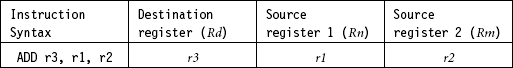
ARM instructions process data held in registers and only access memory with load and store instructions. ARM instructions commonly take two or three operands. For instance the ADD instruction below adds the two values stored in registers r1 and r2 (the source registers). It writes the result to register r3 (the destination register).
In the following sections we examine the function and syntax of the ARM instructions by instruction class—data processing instructions, branch instructions, load-store instructions, software interrupt instruction, and program status register instructions.
3.1 DATA PROCESSING INSTRUCTIONS
The data processing instructions manipulate data within registers. They are move instructions, arithmetic instructions, logical instructions, comparison instructions, and multiply instructions. Most data processing instructions can process one of their operands using the barrel shifter.
If you use the S suffix on a data processing instruction, then it updates the flags in the cpsr. Move and logical operations update the carry flag C, negative flag N, and zero flag Z. The carry flag is set from the result of the barrel shift as the last bit shifted out. The N flag is set to bit 31 of the result. The Z flag is set if the result is zero.
3.1.1 MOVE INSTRUCTIONS
Move is the simplest ARM instruction. It copies N into a destination register Rd, where N is a register or immediate value. This instruction is useful for setting initial values and transferring data between registers.
![]()
| MOV | Move a 32-bit value into a register | Rd = N |
| MVN | move the NOT of the 32-bit value into a register | Rd = ∼N |
Table 3.3, to be presented in Section 3.1.2, gives a full description of the values allowed for the second operand N for all data processing instructions. Usually it is a register Rm or a constant preceded by #.
Table 3.3
Barrel shift operation syntax for data processing instructions.
| N shift operations | Syntax |
| Immediate | #immediate |
| Register | Rm |
| Logical shift left by immediate | Rm, LSL #shift_imm |
| Logical shift left by register | Rm, LSL Rs |
| Logical shift right by immediate | Rm, LSR #shift_imm |
| Logical shift right with register | Rm, LSR Rs |
| Arithmetic shift right by immediate | Rm, ASR #shift_imm |
| Arithmetic shift right by register | Rm, ASR Rs |
| Rotate right by immediate | Rm, ROR #shift_imm |
| Rotate right by register | Rm, ROR Rs |
| Rotate right with extend | Rm, RRX |
3.1.2 BARREL SHIFTER
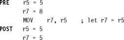
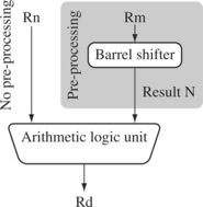
In Example 3.1 we showed a MOV instruction where N is a simple register. But N can be more than just a register or immediate value; it can also be a register Rm that has been preprocessed by the barrel shifter prior to being used by a data processing instruction.
Data processing instructions are processed within the arithmetic logic unit (ALU). A unique and powerful feature of the ARM processor is the ability to shift the 32-bit binary pattern in one of the source registers left or right by a specific number of positions before it enters the ALU. This shift increases the power and flexibility of many data processing operations.
There are data processing instructions that do not use the barrel shift, for example, the MUL (multiply), CLZ (count leading zeros), and QADD (signed saturated 32-bit add) instructions.
Pre-processing or shift occurs within the cycle time of the instruction. This is particularly useful for loading constants into a register and achieving fast multiplies or division by a power of 2.
To illustrate the barrel shifter we will take the example in Figure 3.1 and add a shift operation to the move instruction example. Register Rn enters the ALU without any preprocessing of registers. Figure 3.1 shows the data flow between the ALU and the barrel shifter.
EXAMPLE 3.2
We apply a logical shift left (LSL) to register Rm before moving it to the destination register. This is the same as applying the standard C language shift operator ![]() to the register. The MOV instruction copies the shift operator result N into register Rd. N represents the result of the LSL operation described in Table 3.2.
to the register. The MOV instruction copies the shift operator result N into register Rd. N represents the result of the LSL operation described in Table 3.2.
![]()
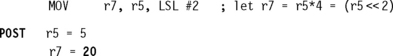
The example multiplies register r5 by four and then places the result into register r7.
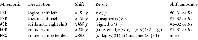
The five different shift operations that you can use within the barrel shifter are summarized in Table 3.2.
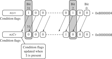
Figure 3.2 illustrates a logical shift left by one. For example, the contents of bit 0 are shifted to bit 1. Bit 0 is cleared. The C flag is updated with the last bit shifted out of the register. This is bit (32 – y) of the original value, where y is the shift amount. When y is greater than one, then a shift by y positions is the same as a shift by one position executed y times.
EXAMPLE 3.3
This example of a MOVS instruction shifts register r1 left by one bit. This multiplies register r1 by a value 21. As you can see, the C flag is updated in the cpsr because the S suffix is present in the instruction mnemonic.
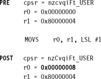
Table 3.3 lists the syntax for the different barrel shift operations available on data processing instructions. The second operand N can be an immediate constant preceded by #, a register value Rm, or the value of Rm processed by a shift.
3.1.3 ARITHMETIC INSTRUCTIONS
The arithmetic instructions implement addition and subtraction of 32-bit signed and unsigned values.
![]()
| ADC | add two 32-bit values and carry | Rd = Rn + N + carry |
| ADD | add two 32-bit values | Rd = Rn + N |
| RSB | reverse subtract of two 32-bit values | Rd = N − Rn |
| RSC | reverse subtract with carry of two 32-bit values | Rd = N − Rn − ! (carry flag) |
| SBC | subtract with carry of two 32-bit values | Rd = Rn − N − ! (carry flag) |
| SUB | subtract two 32-bit values | Rd = Rn − N |
N is the result of the shifter operation. The syntax of shifter operation is shown in Table 3.3.
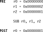
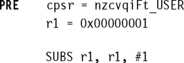
EXAMPLE 3.4
This simple subtract instruction subtracts a value stored in register r2 from a value stored in register r1. The result is stored in register r0.

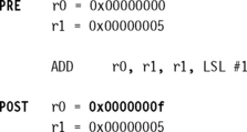
3.1.4 USING THE BARREL SHIFTER WITH ARITHMETIC INSTRUCTIONS
The wide range of second operand shifts available on arithmetic and logical instructions is a very powerful feature of the ARM instruction set. Example 3.7 illustrates the use of the inline barrel shifter with an arithmetic instruction. The instruction multiplies the value stored in register r1 by three.
3.1.5 LOGICAL INSTRUCTIONS
Logical instructions perform bitwise logical operations on the two source registers.
![]()
| AND | logical bitwise AND of two 32-bit values | Rd = Rn & N |
| ORR | logical bitwise OR of two 32-bit values | Rd = Rn | N |
| EOR | logical exclusive OR of two 32-bit values | Rd = Rn ^ N |
| BIC | logical bit clear (AND NOT) | Rd = Rn & ∼N |
EXAMPLE 3.8
This example shows a logical OR operation between registers r1 and r2. r0 holds the result.
![]()
![]()
EXAMPLE 3.9
This example shows a more complicated logical instruction called BIC, which carries out a logical bit clear.
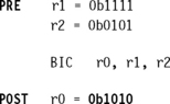
![]()
In this example, register r2 contains a binary pattern where every binary 1 in r2 clears a corresponding bit location in register r1. This instruction is particularly useful when clearing status bits and is frequently used to change interrupt masks in the cpsr.
The logical instructions update the cpsr flags only if the S suffix is present. These instructions can use barrel-shifted second operands in the same way as the arithmetic instructions.
3.1.6 COMPARISON INSTRUCTIONS
The comparison instructions are used to compare or test a register with a 32-bit value. They update the cpsr flag bits according to the result, but do not affect other registers. After the bits have been set, the information can then be used to change program flow by using conditional execution. For more information on conditional execution take a look at Section 3.8. You do not need to apply the S suffix for comparison instructions to update the flags.
![]()
| CMN | compare negated | flags set as a result of Rn + N |
| CMP | compare | flags set as a result of Rn − N |
| TEQ | test for equality of two 32-bit values | flags set as a result of Rn ^ N |
| TST | test bits of a 32-bit value | flags set as a result of Rn & N |
N is the result of the shifter operation. The syntax of shifter operation is shown in Table 3.3.
EXAMPLE 3.10
This example shows a CMP comparison instruction. You can see that both registers, r0 and r9, are equal before executing the instruction. The value of the z flag prior to execution is 0 and is represented by a lowercase z. After execution the z flag changes to 1 or an uppercase Z. This change indicates equality.
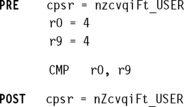
The CMP is effectively a subtract instruction with the result discarded; similarly the TST instruction is a logical AND operation, and TEQ is a logical exclusive OR operation. For each, the results are discarded but the condition bits are updated in the cpsr. It is important to understand that comparison instructions only modify the condition flags of the cpsr and do not affect the registers being compared.
3.1.7 MULTIPLY INSTRUCTIONS
The multiply instructions multiply the contents of a pair of registers and, depending upon the instruction, accumulate the results in with another register. The long multiplies accumulate onto a pair of registers representing a 64-bit value. The final result is placed in a destination register or a pair of registers.
![]()
| MLA | multiply and accumulate | Rd = (Rm*Rs) + Rn |
| MUL | multiply | Rd = Rm*Rs |
![]()
| SMLAL | signed multiply accumulate long | [RdHi, RdLo] = [RdHi, RdLo] + (Rm *Rs) |
| SMULL | signed multiply long | [RdHi, RdLo] = Rm *Rs |
| UMLAL | unsigned multiply accumulate long | [RdHi, RdLo] = [RdHi, RdLo] + (Rm *Rs) |
| UMULL | unsigned multiply long | [RdHi, RdLo] = Rm *Rs |
The number of cycles taken to execute a multiply instruction depends on the processor implementation. For some implementations the cycle timing also depends on the value in Rs. For more details on cycle timings, see Appendix D.
EXAMPLE 3.11
This example shows a simple multiply instruction that multiplies registers r1 and r2 together and places the result into register r0. In this example, register r1 is equal to the value 2, and r2 is equal to 2. The result, 4, is then placed into register r0.

The long multiply instructions (SMLAL, SMULL, UMLAL, and UMULL) produce a 64-bit result. The result is too large to fit a single 32-bit register so the result is placed in two registers labeled RdLo and RdHi. RdLo holds the lower 32 bits of the 64-bit result, and RdHi holds the higher 32 bits of the 64-bit result. Example 3.12 shows an example of a long unsigned multiply instruction.
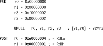
3.2 BRANCH INSTRUCTIONS
A branch instruction changes the flow of execution or is used to call a routine. This type of instruction allows programs to have subroutines, if-then-else structures, and loops. The change of execution flow forces the program counter pc to point to a new address. The ARMv5E instruction set includes four different branch instructions.
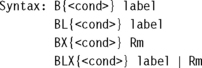
The address label is stored in the instruction as a signed pc-relative offset and must be within approximately 32 MB of the branch instruction. T refers to the Thumb bit in the cpsr. When instructions set T, the ARM switches to Thumb state.
EXAMPLE 3.13
This example shows a forward and backward branch. Because these loops are address specific, we do not include the pre- and post-conditions. The forward branch skips three instructions. The backward branch creates an infinite loop.
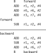
Branches are used to change execution flow. Most assemblers hide the details of a branch instruction encoding by using labels. In this example, forward and backward are the labels. The branch labels are placed at the beginning of the line and are used to mark an address that can be used later by the assembler to calculate the branch offset.
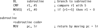
EXAMPLE 3.14
The branch with link, or BL, instruction is similar to the B instruction but overwrites the link register lr with a return address. It performs a subroutine call. This example shows a simple fragment of code that branches to a subroutine using the BL instruction. To return from a subroutine, you copy the link register to the pc.
The branch exchange (BX) and branch exchange with link (BLX) are the third type of branch instruction. The BX instruction uses an absolute address stored in register Rm. It is primarily used to branch to and from Thumb code, as shown in Chapter 4. The T bit in the cpsr is updated by the least significant bit of the branch register. Similarly the BLX instruction updates the T bit of the cpsr with the least significant bit and additionally sets the link register with the return address.
3.3 LOAD-STORE INSTRUCTIONS
Load-store instructions transfer data between memory and processor registers. There are three types of load-store instructions: single-register transfer, multiple-register transfer, and swap.
3.3.1 SINGLE-REGISTER TRANSFER
These instructions are used for moving a single data item in and out of a register. The datatypes supported are signed and unsigned words (32-bit), halfwords (16-bit), and bytes. Here are the various load-store single-register transfer instructions.

| LDR | load word into a register | Rd <- mem32[address] |
| STR | save byte or word from a register | Rd -> mem32[address] |
| LDRB | load byte into a register | Rd <- mem8[address] |
| STRB | save byte from a register | Rd -> mem8[address] |
| LDRH | load halfword into a register | Rd <- mem16[address] |
| STRH | save halfword into a register | Rd -> mem16[address] |
| LDRSB | load signed byte into a register | Rd <- SignExtend (mem8[address]) |
| LDRSH | load signed halfword into a register | Rd <- SignExtend (mem16[address]) |
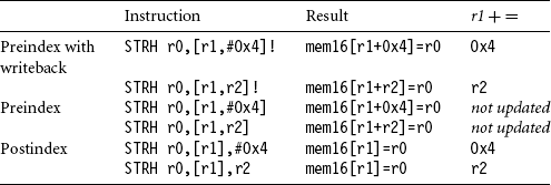
Tables 3.5 and 3.7, to be presented is Section 3.3.2, describe the addressing1 and addressing2 syntax.
Table 3.5
Single-register load-store addressing, word or unsigned byte.
| Addressing1 mode and index method | Addressing1 syntax |
| Preindex with immediate offset | [Rn, #+/-offset_12] |
| Preindex with register offset | [Rn, +/-Rm] |
| Preindex with scaled register offset | [Rn, +/-Rm, shift #shift_imm] |
| Preindex writeback with immediate offset | [Rn, #+/-offset_12]! |
| Preindex writeback with register offset | [Rn, +/-Rm]! |
| Preindex writeback with scaled register offset | [Rn, +/-Rm, shift #shift_imm]! |
| Immediate postindexed | [Rn], #+/-offset_12 |
| Register postindex | [Rn], +/-Rm |
| Scaled register postindex | [Rn], +/-Rm, shift #shift_imm |
Table 3.7
Single-register load-store addressing, halfword, signed halfword, signed byte, and doubleword.
| Addressing2 mode and index method | Addressing2 syntax |
| Preindex immediate offset | [Rn, #+/-offset_8] |
| Preindex register offset | [Rn, +/-Rm] |
| Preindex writeback immediate offset | [Rn, #+/-offset_8]! |
| Preindex writeback register offset | [Rn, +/-Rm]! |
| Immediate postindexed | [Rn], #+/-offset_8 |
| Register postindexed | [Rn], +/-Rm |
EXAMPLE 3.15
LDR and STR instructions can load and store data on a boundary alignment that is the same as the datatype size being loaded or stored. For example, LDR can only load 32-bit words on a memory address that is a multiple of four bytes—0, 4, 8, and so on. This example shows a load from a memory address contained in register r1, followed by a store back to the same address in memory.

The first instruction loads a word from the address stored in register r1 and places it into register r0. The second instruction goes the other way by storing the contents of register r0 to the address contained in register r1. The offset from register r1 is zero. Register r1 is called the base address register.
3.3.2 SINGLE-REGISTER LOAD-STORE ADDRESSING MODES
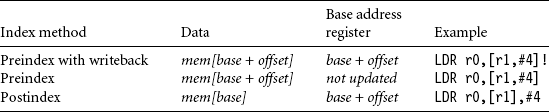
The ARM instruction set provides different modes for addressing memory. These modes incorporate one of the indexing methods: preindex with writeback, preindex, and postindex (see Table 3.4).
Table 3.4
Note: ! indicates that the instruction writes the calculated address back to the base address register.
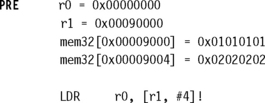
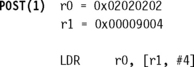
EXAMPLE 3.16
Preindex with writeback calculates an address from a base register plus address offset and then updates that address base register with the new address. In contrast, the preindex offset is the same as the preindex with writeback but does not update the address base register. Postindex only updates the address base register after the address is used. The preindex mode is useful for accessing an element in a data structure. The postindex and preindex with writeback modes are useful for traversing an array.
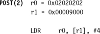
![]()
Example 3.15 used a preindex method. This example shows how each indexing method effects the address held in register r1, as well as the data loaded into register r0. Each instruction shows the result of the index method with the same pre-condition.
The addressing modes available with a particular load or store instruction depend on the instruction class. Table 3.5 shows the addressing modes available for load and store of a 32-bit word or an unsigned byte.
A signed offset or register is denoted by “+/−”, identifying that it is either a positive or negative offset from the base address register Rn. The base address register is a pointer to a byte in memory, and the offset specifies a number of bytes.
Immediate means the address is calculated using the base address register and a 12-bit offset encoded in the instruction. Register means the address is calculated using the base address register and a specific register’s contents. Scaled means the address is calculated using the base address register and a barrel shift operation.
Table 3.6 provides an example of the different variations of the LDR instruction. Table 3.7 shows the addressing modes available on load and store instructions using 16-bit halfword or signed byte data.
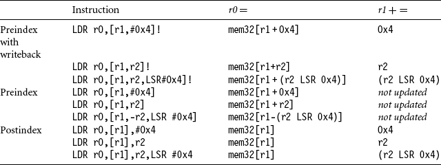
These operations cannot use the barrel shifter. There are no STRSB or STRSH instructions since STRH stores both a signed and unsigned halfword; similarly STRB stores signed and unsigned bytes. Table 3.8 shows the variations for STRH instructions.
3.3.3 MULTIPLE-REGISTER TRANSFER
Load-store multiple instructions can transfer multiple registers between memory and the processor in a single instruction. The transfer occurs from a base address register Rn pointing into memory. Multiple-register transfer instructions are more efficient from single-register transfers for moving blocks of data around memory and saving and restoring context and stacks.
Load-store multiple instructions can increase interrupt latency. ARM implementations do not usually interrupt instructions while they are executing. For example, on an ARM7 a load multiple instruction takes 2 + Nt cycles, where N is the number of registers to load and t is the number of cycles required for each sequential access to memory. If an interrupt has been raised, then it has no effect until the load-store multiple instruction is complete.
Compilers, such as armcc, provide a switch to control the maximum number of registers being transferred on a load-store, which limits the maximum interrupt latency.
![]()
| LDM | load multiple registers | {Rd}N * <- mem32[start address + 4*N] optional Rn updated |
| STM | save multiple registers | {Rd}N * -> mem32[start address + 4*N] optional Rn updated |
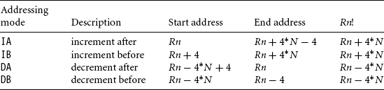
Table 3.9 shows the different addressing modes for the load-store multiple instructions. Here N is the number of registers in the list of registers.
Any subset of the current bank of registers can be transferred to memory or fetched from memory. The base register Rn determines the source or destination address for a load-store multiple instruction. This register can be optionally updated following the transfer. This occurs when register Rn is followed by the ! character, similiar to the single-register load-store using preindex with writeback.
EXAMPLE 3.17
In this example, register r0 is the base register Rn and is followed by !, indicating that the register is updated after the instruction is executed. You will notice within the load multiple instruction that the registers are not individually listed. Instead the “-” character is used to identify a range of registers. In this case the range is from register r1 to r3 inclusive.
Each register can also be listed, using a comma to separate each register within “{” and “}” brackets.
![]()
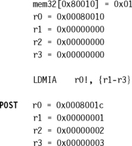
Figure 3.3 shows a graphical representation.
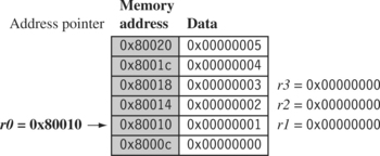
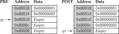
The base register r0 points to memory address 0x80010 in the PRE condition. Memory addresses 0x80010, 0x80014, and 0x80018 contain the values 1, 2, and 3 respectively. After the load multiple instruction executes registers r1, r2, and r3 contain these values as shown in Figure 3.4. The base register r0 now points to memory address 0x8001c after the last loaded word.
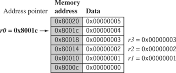
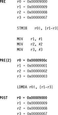
Now replace the LDMIA instruction with a load multiple and increment before LDMIB instruction and use the same PRE conditions. The first word pointed to by register r0 is ignored and register r1 is loaded from the next memory location as shown in Figure 3.5.
After execution, register r0 now points to the last loaded memory location. This is in contrast with the LDMIA example, which pointed to the next memory location.
The decrement versions DA and DB of the load-store multiple instructions decrement the start address and then store to ascending memory locations. This is equivalent to descending memory but accessing the register list in reverse order. With the increment and decrement load multiples, you can access arrays forwards or backwards. They also allow for stack push and pull operations, illustrated later in this section.
Table 3.10 shows a list of load-store multiple instruction pairs. If you use a store with base update, then the paired load instruction of the same number of registers will reload the data and restore the base address pointer. This is useful when you need to temporarily save a group of registers and restore them later.
Table 3.10
Load-store multiple pairs when base update used.
| Store multiple | Load multiple |
| STMIA | LDMDB |
| STMIB | LDMDA |
| STMDA | LDMIB |
| STMDB | LDMIA |
EXAMPLE 3.18
This example shows an STM increment before instruction followed by an LDM decrement after instruction.
The STMIB instruction stores the values 7, 8, 9 to memory. We then corrupt register r1 to r3. The LDMDA reloads the original values and restores the base pointer r0.
EXAMPLE 3.19
We illustrate the use of the load-store multiple instructions with a block memory copy example. This example is a simple routine that copies blocks of 32 bytes from a source address location to a destination address location.
The example has two load-store multiple instructions, which use the same increment after addressing mode.
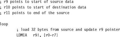
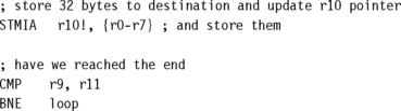
This routine relies on registers r9, r10, and r11 being set up before the code is executed. Registers r9 and r11 determine the data to be copied, and register r10 points to the destination in memory for the data. LDMIA loads the data pointed to by register r9 into registers r0 to r7. It also updates r9 to point to the next block of data to be copied. STMIA copies the contents of registers r0 to r7 to the destination memory address pointed to by register r10. It also updates r10 to point to the next destination location. CMP and BNE compare pointers r9 and r11 to check whether the end of the block copy has been reached. If the block copy is complete, then the routine finishes; otherwise the loop repeats with the updated values of register r9 and r10.
The BNE is the branch instruction B with a condition mnemonic NE (not equal). If the previous compare instruction sets the condition flags to not equal, the branch instruction is executed.
Figure 3.6 shows the memory map of the block memory copy and how the routine moves through memory. Theoretically this loop can transfer 32 bytes (8 words) in two instructions, for a maximum possible throughput of 46 MB/second being transferred at 33 MHz. These numbers assume a perfect memory system with fast memory.
3.3.3.1 Stack Operations
The ARM architecture uses the load-store multiple instructions to carry out stack operations. The pop operation (removing data from a stack) uses a load multiple instruction; similarly, the push operation (placing data onto the stack) uses a store multiple instruction.
When using a stack you have to decide whether the stack will grow up or down in memory. A stack is either ascending (A) or descending (D). Ascending stacks grow towards higher memory addresses; in contrast, descending stacks grow towards lower memory addresses.
When you use a full stack (F), the stack pointer sp points to an address that is the last used or full location (i.e., sp points to the last item on the stack). In contrast, if you use an empty stack (E) the sp points to an address that is the first unused or empty location (i.e., it points after the last item on the stack).
There are a number of load-store multiple addressing mode aliases available to support stack operations (see Table 3.11). Next to the pop column is the actual load multiple instruction equivalent. For example, a full ascending stack would have the notation FA appended to the load multiple instruction—LDMFA. This would be translated into an LDMDA instruction.
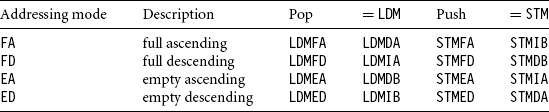
ARM has specified an ARM-Thumb Procedure Call Standard (ATPCS) that defines how routines are called and how registers are allocated. In the ATPCS, stacks are defined as being full descending stacks. Thus, the LDMFD and STMFD instructions provide the pop and push functions, respectively.
EXAMPLE 3.20
The STMFD instruction pushes registers onto the stack, updating the sp. Figure 3.7 shows a push onto a full descending stack. You can see that when the stack grows the stack pointer points to the last full entry in the stack.


![]()
EXAMPLE 3.21
In contrast, Figure 3.8 shows a push operation on an empty stack using the STMED instruction. The STMED instruction pushes the registers onto the stack but updates register sp to point to the next empty location.

When handling a checked stack there are three attributes that need to be preserved: the stack base, the stack pointer, and the stack limit. The stack base is the starting address of the stack in memory. The stack pointer initially points to the stack base; as data is pushed onto the stack, the stack pointer descends memory and continuously points to the top of stack. If the stack pointer passes the stack limit, then a stack overflow error has occurred. Here is a small piece of code that checks for stack overflow errors for a descending stack:
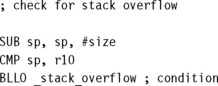
ATPCS defines register r10 as the stack limit or sl. This is optional since it is only used when stack checking is enabled. The BLL0 instruction is a branch with link instruction plus the condition mnemonic L0. If sp is less than register r10 after the new items are pushed onto the stack, then stack overflow error has occurred. If the stack pointer goes back past the stack base, then a stack underflow error has occurred.
3.3.4 SWAP INSTRUCTION
The swap instruction is a special case of a load-store instruction. It swaps the contents of memory with the contents of a register. This instruction is an atomic operation—it reads and writes a location in the same bus operation, preventing any other instruction from reading or writing to that location until it completes.
![]()
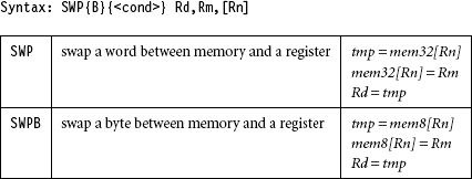
Swap cannot be interrupted by any other instruction or any other bus access. We say the system “holds the bus” until the transaction is complete.
EXAMPLE 3.22
The swap instruction loads a word from memory into register r0 and overwrites the memory with register r1.
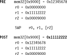
This instruction is particularly useful when implementing semaphores and mutual exclusion in an operating system. You can see from the syntax that this instruction can also have a byte size qualifier B, so this instruction allows for both a word and a byte swap.
EXAMPLE 3.23
This example shows a simple data guard that can be used to protect data from being written by another task. The SWP instruction “holds the bus” until the transaction is complete.

The address pointed to by the semaphore either contains the value 0 or 1. When the semaphore equals 1, then the service in question is being used by another process. The routine will continue to loop around until the service is released by the other process—in other words, when the semaphore address location contains the value 0.
3.4 SOFTWARE INTERRUPT INSTRUCTION
A software interrupt instruction (SWI) causes a software interrupt exception, which provides a mechanism for applications to call operating system routines.
![]()
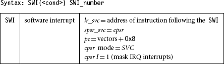
When the processor executes an SWI instruction, it sets the program counter pc to the offset 0×8 in the vector table. The instruction also forces the processor mode to SVC, which allows an operating system routine to be called in a privileged mode.
Each SWI instruction has an associated SWI number, which is used to represent a particular function call or feature.
EXAMPLE 3.24
Here we have a simple example of an SWI call with SWI number 0x123456, used by ARM toolkits as a debugging SWI. Typically the SWI instruction is executed in user mode.
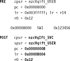
Since SWI instructions are used to call operating system routines, you need some form of parameter passing. This is achieved using registers. In this example, register r0 is used to pass the parameter 0x12. The return values are also passed back via registers.
Code called the SWI handler is required to process the SWI call. The handler obtains the SWI number using the address of the executed instruction, which is calculated from the link register lr.
The SWI number is determined by
![]()
Here the SWI instruction is the actual 32-bit SWI instruction executed by the processor.
EXAMPLE 3.25
This example shows the start of an SWI handler implementation. The code fragment determines what SWI number is being called and places that number into register r10. You can see from this example that the load instruction first copies the complete SWI instruction into register r10. The BIC instruction masks off the top bits of the instruction, leaving the SWI number. We assume the SWI has been called from ARM state.
![]()
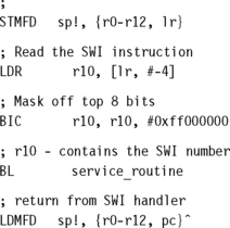
The number in register r10 is then used by the SWI handler to call the appropriate SWI service routine.
3.5 PROGRAM STATUS REGISTER INSTRUCTIONS
The ARM instruction set provides two instructions to directly control a program status register (psr). The MRS instruction transfers the contents of either the cpsr or spsr into a register; in the reverse direction, the MSR instruction transfers the contents of a register into the cpsr or spsr. Together these instructions are used to read and write the cpsr and spsr.
In the syntax you can see a label called fields. This can be any combination of control (c), extension (x), status (s), and flags (f). These fields relate to particular byte regions in a psr, as shown in Figure 3.9.
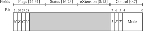
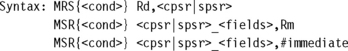
| MRS | copy program status register to a general-purpose register | Rd = psr |
| MSR | move a general-purpose register to a program status register | psr[field] = Rm |
| MSR | move an immediate value to a program status register | psr[field] = immediate |
The c field controls the interrupt masks, Thumb state, and processor mode. Example 3.26 shows how to enable IRQ interrupts by clearing the I mask. This operation involves using both the MRS and MSR instructions to read from and then write to the cpsr.
EXAMPLE 3.26
The MSR first copies the cpsr into register r1. The BIC instruction clears bit 7 of r1. Register r1 is then copied back into the cpsr, which enables IRQ interrupts. You can see from this example that this code preserves all the other settings in the cpsr and only modifies the I bit in the control field.
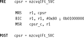
This example is in SVC mode. In user mode you can read all cpsr bits, but you can only update the condition flag field f.
3.5.1 COPROCESSOR INSTRUCTIONS
Coprocessor instructions are used to extend the instruction set. A coprocessor can either provide additional computation capability or be used to control the memory subsystem including caches and memory management. The coprocessor instructions include data processing, register transfer, and memory transfer instructions. We will provide only a short overview since these instructions are coprocessor specific. Note that these instructions are only used by cores with a coprocessor.
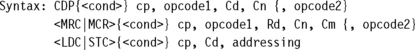
| CDP | coprocessor data processing—perform an operation in a coprocessor |
| MRC MCR | coprocessor register transfer—move data to/from coprocessor registers |
| LDC STC | coprocessor memory transfer—load and store blocks of memory to/from a coprocessor |
In the syntax of the coprocessor instructions, the cp field represents the coprocessor number between p0 and p15. The opcode fields describe the operation to take place on the coprocessor. The Cn, Cm, and Cd fields describe registers within the coprocessor. The coprocessor operations and registers depend on the specific coprocessor you are using. Coprocessor 15 (CP15) is reserved for system control purposes, such as memory management, write buffer control, cache control, and identification registers.
3.5.2 COPROCESSOR 15 INSTRUCTION SYNTAX
CP15 configures the processor core and has a set of dedicated registers to store configuration information, as shown in Example 3.27. A value written into a register sets a configuration attribute—for example, switching on the cache.
CP15 is called the system control coprocessor. Both MRC and MCR instructions are used to read and write to CP15, where register Rd is the core destination register, Cn is the primary register, Cm is the secondary register, and opcode2 is a secondary register modifier. You may occasionally hear secondary registers called “extended registers.”
As an example, here is the instruction to move the contents of CP15 control register c1 into register r1 of the processor core:
![]()
We use a shorthand notation for CP15 reference that makes referring to configuration registers easier to follow. The reference notation uses the following format:
![]()
The first term, CP15, defines it as coprocessor 15. The second term, after the separating colon, is the primary register. The primary register X can have a value between 0 and 15. The third term is the secondary or extended register. The secondary register Y can have a value between 0 and 15. The last term, opcode2, is an instruction modifier and can have a value between 0 and 7. Some operations may also use a nonzero value w of opcode1. We write these as CP15:w:cX:cY:Z.
3.6 LOADING CONSTANTS
You might have noticed that there is no ARM instruction to move a 32-bit constant into a register. Since ARM instructions are 32 bits in size, they obviously cannot specify a general 32-bit constant.
To aid programming there are two pseudoinstructions to move a 32-bit value into a register.
![]()
| LDR | load constant pseudoinstruction | Rd = 32-bit constant |
| ADR | load address pseudoinstruction | Rd = 32-bit relative address |
The first pseudoinstruction writes a 32-bit constant to a register using whatever instructions are available. It defaults to a memory read if the constant cannot be encoded using other instructions.
The second pseudoinstruction writes a relative address into a register, which will be encoded using a pc-relative expression.
EXAMPLE 3.28
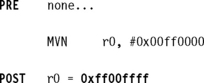
This example shows an LDR instruction loading a 32-bit constant 0xff00ffff into register r0.
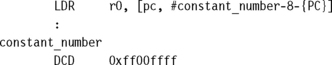
This example involves a memory access to load the constant, which can be expensive for time-critical routines.
Example 3.29 shows an alternative method to load the same constant into register r0 by using an MVN instruction.
As you can see, there are alternatives to accessing memory, but they depend upon the constant you are trying to load. Compilers and assemblers use clever techniques to avoid loading a constant from memory. These tools have algorithms to find the optimal number of instructions required to generate a constant in a register and make extensive use of the barrel shifter. If the tools cannot generate the constant by these methods, then it is loaded from memory. The LDR pseudoinstruction either inserts an MOV or MVN instruction to generate a value (if possible) or generates an LDR instruction with a pc-relative address to read the constant from a literal pool—a data area embedded within the code.
Table 3.12 shows two pseudocode conversions. The first conversion produces a simple MOV instruction; the second conversion produces a pc-relative load. We recommended that you use this pseudoinstruction to load a constant. To see how the assembler has handled a particular load constant, you can pass the output through a disassembler, which will list the instruction chosen by the tool to load the constant.
Table 3.12
LDR pseudoinstruction conversion.
| Pseudoinstruction | Actual instruction |
| LDR r0, =0xff | MOV r0, #0xff |
| LDR r0, =0x55555555 | LDR r0, [pc, #offset_12] |
Another useful pseudoinstruction is the ADR instruction, or address relative. This instruction places the address of the given label into register Rd, using a pc-relative add or subtract.
3.7 ARMV5E EXTENSIONS
The ARMv5E extensions provide many new instructions (see Table 3.13). One of the most important additions is the signed multiply accumulate instructions that operate on 16-bit data. These operations are single cycle on many ARMv5E implementations.
Table 3.13
New instructions provided by the ARMv5E extensions.
| Instruction | Description |
| CLZ {<cond>} Rd, Rm | count leading zeros |
| QADD {<cond>} Rd, Rm, Rn | signed saturated 32-bit add |
| QDADD{<cond>} Rd, Rm, Rn | signed saturated double 32-bit add |
| QDSUB{<cond>} Rd, Rm, Rn | signed saturated double 32-bit subtract |
| QSUB{<cond>} Rd, Rm, Rn | signed saturated 32-bit subtract |
| SMLAxy{<cond>} Rd, Rm, Rs, Rn | signed multiply accumulate 32-bit (1) |
| SMLALxy{<cond>} RdLo, RdHi, Rm, Rs | signed multiply accumulate 64-bit |
| SMLAWy{<cond>} Rd, Rm, Rs, Rn | signed multiply accumulate 32-bit (2) |
| SMULxy{<cond>} Rd, Rm, Rs | signed multiply (1) |
| SMULWy{<cond>} Rd, Rm, Rs | signed multiply (2) |
ARMv5E provides greater flexibility and efficiency when manipulating 16-bit values, which is important for applications such as 16-bit digital audio processing.
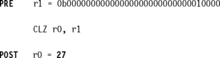
3.7.1 COUNT LEADING ZEROS INSTRUCTION
The count leading zeros instruction counts the number of zeros between the most significant bit and the first bit set to 1. Example 3.30 shows an example of a CLZ instruction.
3.7.2 SATURATED ARITHMETIC
Normal ARM arithmetic instructions wrap around when you overflow an integer value. For example, 0x7fffffff + 1 = -0x80000000. Thus, when you design an algorithm, you have to be careful not to exceed the maximum representable value in a 32-bit integer.
EXAMPLE 3.31
This example shows what happens when the maximum value is exceeded.
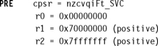
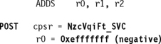
In the example, registers r1 and r2 contain positive numbers. Register r2 is equal to 0x7fffffff, which is the maximum positive value you can store in 32 bits. In a perfect world adding these numbers together would result in a large positive number. Instead the value becomes negative and the overflow flag, V, is set.
In contrast, using the ARMv5E instructions you can saturate the result—once the highest number is exceeded the results remain at the maximum value of 0x7fffffff. This avoids the requirement for any additional code to check for possible overflows. Table 3.14 lists all the ARMv5E saturation instructions.
Table 3.14
| Instruction | Saturated calculation |
| QADD | Rd = Rn + Rm |
| QDADD | Rd = Rn + (Rm*2) |
| QSUB | Rd = Rn – Rm |
| QDSUB | Rd = Rn – (Rm*2) |
EXAMPLE 3.32
This example shows the same data being passed into the QADD instruction.
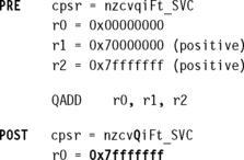
You will notice that the saturated number is returned in register r0. Also the Q bit (bit 27 of the cpsr) has been set, indicating saturation has occurred. The Q flag is sticky and will remain set until explicitly cleared.
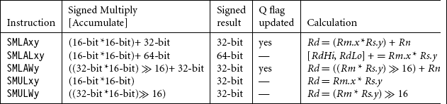
3.7.3 ARMv5E MULTIPLY INSTRUCTIONS
Table 3.15 shows a complete list of the ARMv5E multiply instructions. In the table, x and y select which 16 bits of a 32-bit register are used for the first and second operands, respectively. These fields are set to a letter T for the top 16-bits, or the letter B for the bottom 16 bits. For multiply accumulate operations with a 32-bit result, the Q flag indicates if the accumulate overflowed a signed 32-bit value.
EXAMPLE 3.33
This example shows how you use these operations. The example uses a signed multiply accumulate instruction, SMLATB.
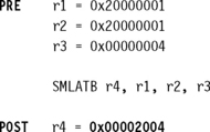
The instruction multiplies the top 16 bits of register r1 by the bottom 16 bits of register r2. It adds the result to register r3 and writes it to destination register r4.
3.8 CONDITIONAL EXECUTION
Most ARM instructions are conditionally executed—you can specify that the instruction only executes if the condition code flags pass a given condition or test. By using conditional execution instructions you can increase performance and code density.
The condition field is a two-letter mnemonic appended to the instruction mnemonic. The default mnemonic is AL, or always execute.
Conditional execution reduces the number of branches, which also reduces the number of pipeline flushes and thus improves the performance of the executed code. Conditional execution depends upon two components: the condition field and condition flags. The condition field is located in the instruction, and the condition flags are located in the cpsr.
EXAMPLE 3.34
This example shows an ADD instruction with the EQ condition appended. This instruction will only be executed when the zero flag in the cpsr is set to 1.
![]()
Only comparison instructions and data processing instructions with the S suffix appended to the mnemonic update the condition flags in the cpsr.
EXAMPLE 3.35
To help illustrate the advantage of conditional execution, we will take the simple C code fragment shown in this example and compare the assembler output using nonconditional and conditional instructions.

Let register r1 represent a and register r2 represent b. The following code fragment shows the same algorithm written in ARM assembler. This example only uses conditional execution on the branch instructions:

Now compare the same code with full conditional execution. As you can see, this dramatically reduces the number of instructions:
![]()
![]()
3.9 SUMMARY
In this chapter we covered the ARM instruction set. All ARM instructions are 32 bits in length. The arithmetic, logical, comparisons, and move instructions can all use the inline barrel shifter, which pre-processes the second register Rm before it enters into the ALU.
The ARM instruction set has three types of load-store instructions: single-register load-store, multiple-register load-store, and swap. The multiple load-store instructions provide the push-pop operations on the stack. The ARM-Thumb Procedure Call Standard (ATPCS) defines the stack as being a full descending stack.
The software interrupt instruction causes a software interrupt that forces the processor into SVC mode; this instruction invokes privileged operating system routines. The program status register instructions write and read to the cpsr and spsr. There are also special pseudoinstructions that optimize the loading of 32-bit constants.
The ARMv5E extensions include count leading zeros, saturation, and improved multiply instructions. The count leading zeros instruction counts the number of binary zeros before the first binary one. Saturation handles arithmetic calculations that overflow a 32-bit integer value. The improved multiply instructions provide better flexibility in multiplying 16-bit values.
Most ARM instructions can be conditionally executed, which can dramatically reduce the number of instructions required to perform a specific algorithm.