Chapter 3
ESD Power Grid Design
The ESD power grid and metal interconnects have a significant impact on the ESD robustness of the semiconductor chip [1–3]. In the ESD design synthesis, it is important to integrate the interconnects, vias, and power grid effectively with the bond pads, the circuitry, ESD signal pin devices, and ESD power clamp circuitry [2, 3]. In this chapter, the ESD design synthesis of the interconnects and the power grid will be discussed. The discussion will address both practical and analytical examples [1–28].
3.1.1 ESD Power Grid – Key ESD Design Parameters
In the ESD design synthesis of the power grid, there are key ESD design parameters and metrics to consider. These key parameters are to be considered as part of the ESD design synthesis of the power grid:
- Bus Width: The bus width required to survive ESD failure for a given metal layer.
- Bus Resistance: The bus resistance per unit length.
- Across ESD Bus Resistance: The bus resistance across the length of the ESD network.
- Critical Bus Resistance: The worst case bus resistance allowed without failure of the signal pin (can be defined as the breakdown voltage at the signal pin divided by the ESD current through the power bus).
- ESD Signal Pin to ESD Power Clamp Distance: The distance between the ESD signal pin and the ESD power clamp.
- Critical ESD Signal to ESD Power Clamp Resistance: The worst case resistance between the ESD signal pin and the ESD power clamp prior to signal pin failure.
- ESD Power Clamp to ESD Power Clamp Bus Resistance: The resistance between two adjacent ESD power clamps on a given power rail.
- Number of ESD Power Clamps per I/O Cells: The number of required ESD power clamps for the number of signal pins.
- ESD Power Clamp Placement Frequency: The spatial frequency of the placement of the ESD power clamps along the peripheral power rail.
3.1.2 ESD and the Alternative Current Path – The Role of ESD Power Grid Resistance
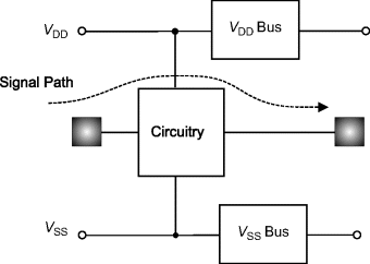
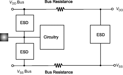
The semiconductor chip design can be simplified as a system with a signal path, and the power grid. The role of the signal path is to have an input signal, process the signal, and have an output signal. For area and speed, the circuits along the signal path are as small as possible to perform this function. The role of the power grid is to supply the power to the circuits to support the necessary power for this function. The circuitry is electrically connected to the power supply (e.g., VDD) and the ground (e.g., VSS). Figure 3.1 shows an example of a system with the signal path highlighted.
Figure 3.1 The signal path
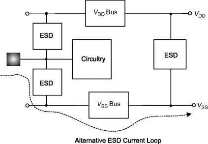
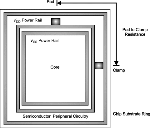
During an ESD event, the signal pins are pulsed with an ESD event where the power rails serve as reference ground potential. For ESD design synthesis, the role of the ESD circuitry is to divert the ESD current other than the signal path. Figure 3.2 shows the semiconductor chip with the alternative current path established with ESD circuitry.
Figure 3.2 The alternative ESD current path
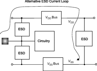
The ESD circuitry establishes an alternative current path to reach the grounded reference. In order for the ESD circuitry to be effective, the alternative current path must have the characteristics of low impedance (or low resistance), as well as being of adequate robustness not to be destroyed during the ESD event below the desired ESD specification levels. The alternative current path, including the power grid, must be able to survive the peak current and energy from the ESD pulse event. The peak current of the ESD event is a function of the ESD specification. The ESD specifications are as follows:
- Human body model (HBM).
- Machine model (MM).
- Charged device model (CDM).
- Human metal model (HMM).
- IEC 61000-4-2.
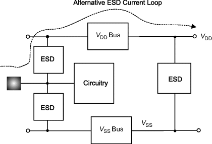
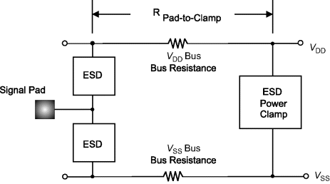
Figure 3.3 shows the ESD Kirchoff current loop to the VDD power supply rail. The figure shows the current flowing from the bond pad, the interconnect between the bond pad and the ESD signal pad device, the interconnect between the ESD device and the power grid, and through the VDD power grid. Each interconnect and element in the path must have low resistance, as well as survive the ESD pulse event.
Figure 3.3 ESD Kirchoff current loop to VDD power rail
The impedance of each element must be low enough to avoid the voltage of the signal pad increasing. In order to prevent failure of the circuitry in the signal path, the bond pad voltage must be kept below the voltage-to-failure, Vf, of the circuitry. Assuming all elements are resistive in nature, according to Kirchoff's voltage law (KVL), the bond pad voltage can be represented as a function of the turn-on voltage, VON, and the IR voltage drop through the alternative current loop:
![]()
Assuming the ESD current flows through all these elements, it can be written as
![]()
This can be represented simply as the voltage drop through the ESD input element, the voltage drop in the power bus, and the voltage drop through the ESD power clamp element. In this case, the current flows through the ESD power clamp placed between VDD and VSS power rails:
![]()
In the case where the grounded reference is the VDD power rail, then it can be represented simply as the voltage drop through the ESD input element connected to the VDD power bus, and the voltage drop in the VDD power bus:
![]()
Figure 3.4 shows the ESD Kirchoff current loop to the VSS power supply rail. The figure shows the current flowing from the bond pad, the interconnect between the bond pad and the ESD signal pad device, the interconnect between the ESD device and the power grid, and through the VSS power grid. Each interconnect and element in the path must have low resistance, as well as survive the ESD pulse event.
Figure 3.4 ESD Kirchoff current loop to VSS rail
In the case where the grounded reference is the VSS power rail, then it can be represented simply as the voltage drop through the ESD input element which is connected to the ground power rail, and the voltage drop in the VSS power bus:
![]()
3.2 Semiconductor Chip Impedance
From an impedance perspective, the bond pad voltage can be represented as a function of the turn-on voltage, VON, and impedance through the alternative current loop:
![]()
Assuming the ESD current flows through all these elements, it can be written as
![]()
The impedance of the power grid can be represented as a lumped or distributed element. As a lumped element, the semiconductor chip can be represented as a capacitor, whose impedance is Zchip = 1/[jωCchip], and the frequency is associated with the characteristic frequency of the ESD event:
![]()
In a semiconductor chip with no ESD power clamps, and a single power domain, the chip capacitance scales with the chip area. In a CMOS chip, half the chip area will be a capacitor formed by the n-well to substrate metallurgical junction. In a large chip, in older technologies, there was no need for an ESD element between the VDD and VSS power rails.
Depending on the resistance of the power grid, the semiconductor chip impedance may be best understood as a distributed element instead of a lumped element [2]. In that case, the semiconductor chip and power bus are to be represented as a resistor–capacitor transmission line [2].
In advanced technologies, small semiconductor chips, or segmented power supply domains, ESD power clamps are introduced in each power domain. In this case, the domains can be represented as a single bus resistance element, and an ESD power clamp for the effective series elements.
3.3 Interconnect Failure and Dynamic on-Resistance
In the ESD design synthesis of interconnects, there are two primary issues. With the design synthesis of the interconnects, the failure of the interconnect is critical to the determination of the interconnect minimum requirements [1–20]. In addition, the DC resistance as well as the dynamic on-resistance is critical to the determination of the satisfactory resistances in the alternative current loop in the semiconductor chip design [1–3].
3.3.1 Interconnect Dynamic On-Resistance
Resistance is defined according to the linear relationship
![]()
where R(T) is the dynamic resistance at temperature T, Ro is the initial resistance, and α is the temperature coefficient of resistance (TCR). From this form, we can solve for temperature in the interconnect, as:
![]()
To relate power and thermal impedance to the resistance, the differential resistance dR(T) is expressed as:
![]()
where we define temperature as the product of the heat fluence and the thermal impedance:
![]()
The total differential of temperature can be expressed as:
![]()
The heat flux is equal to the input power from conservation of energy. Substituting in power for the heat flux, the total differential resistance can be expressed as:
![]()
Since the impedance is constant, and integration of the expression from the initial to final resistance [1, 11–14],
![]()
Hence the normalized resistance change is proportional to the product of the thermal impedance, power, and temperature coefficient of resistance. Combining Joule heating (e.g., P = I2R) and resistance (R = ρL/A), and substituting for the current density, J, then the expression of normalized differential resistance can be expressed as [1, 12–14]:
![]()
From the normalized differential resistance, we can solve for the thermal impedance as:
![]()
From this formulation, the thermal impedance can be extracted from the resistance change and the current density.
3.3.2 Ti/Al/Ti Interconnect Failure
Aluminum interconnects are formed on the planar dielectric film. Aluminum interconnects consist of a refractory metal film below and above the aluminum film. The refractory metal assists in the adhesion of the aluminum with the inter-level dielectric material. Typically, a standard process consists of titanium (Ti), titanium nitride (TiN) – where the TiN provides the adhesion between the dielectric and Ti film. To quantify the ESD robustness of a Ti/Al/Ti interconnect, the geometric definition is important for its evaluation [1, 12].
In a Ti/Al/Ti interconnect, the interconnect cross-section is rectangular. The liner film exists on the top and the bottom of the film, but not on the sides of the interconnect. Since the interconnect is a composite film, with the refractory metal being of a high resistance value, an effective resistivity model can be used where we assume the effective resistivity is [1, 13, 14]:
![]()
where the geometrical dimensions are the liner bottom, δ, and the line height, y.
Assuming a critical energy Ecrit, at which the interconnect failure occurs, this can be related to the product of the average energy input during a pulse event. Assuming that the current is constant during the pulse, time, and the current can be removed from the average, where the average resistance is the mean between the initial and final resistance value [1]:
We can define an expression which is the normalized change in resistance:
![]()
and express the critical energy according to the normalized change in resistance at failure:
![]()
Energy can be related to the heat capacity and heat of fusion [11]:
![]()
Hence, when the temperature is the critical temperature of failure, then the energy expression is the critical energy. From the resistance relationship on temperature, we can substitute for the temperature change as a function of normalized resistance change, and the temperature coefficient of resistance:
![]()
In the case of the composite film, the mass of each region, and specific heat of each film must be defined. In the above development, it implies that the temperature of the composite film is equal. More accurately, we can find the total mass summed over all regions:
![]()
From the two forms of the critical energy, the critical current to failure can be expressed as [1, 12]:
Expanding this expression to address the multiple films (e.g., aluminum, cladding, and insulator materials):
In this expression, the cross-sectional area of the interconnect can be brought into the numerator in order to express the equation as a function of the line width and the geometric variables associated with the films.
The physical volume of the Al region can be expressed as [1, 12]:
![]()
and
![]()
The cladding volume can be expressed as
![]()
The fully passivated thermal sheath volume can be expressed as the volume of the interconnect with the additional dimension associated with the thermal heat volume in the insulator minus the interconnect:
![]()
This form assumes extension beyond the length of the interconnect. This is in the form of:
![]()
and the time-dependent oxide sheath thickness is a function of the pulse width and the heat diffusion coefficient in the oxide:
![]()
In the assumption that the highest-level film is unpassivated, this can be expressed as:
![]()
As an additional assumption, for long-length structures with passivation above and below the interconnect, we can ignore the thermal component on the end of the wires and simplify the analysis to the case of:
![]()
Let the region be such that the indices (e.g., ijk) be in the order of Al, cladding, and the insulator volume, respectively. Expressing this term as a function of the volumes, heat capacity, and density:
3.3.3 Copper Interconnect Failure
In today's advanced high-performance technologies, the need for reduced resistance and capacitance interconnects has led to an evolution from Ti/Al/Ti or Al-based interconnect systems to copper (Cu)-based interconnect systems [1, 13–15, 17, 19]. Copper interconnect systems are formed by providing troughs in the inter-level dielectric (ILD) films. The dielectric is etched using reactive ion etch (RIE) processes, followed by cladding material and Cu film deposition. The cladding, or liner material, is typically a refractory metal film. The cladding serves as a diffusion barrier, and provides adhesion to the insulator film. These materials can include TiN, WN, Ta, TaN, or TaSiN [1].
To quantify the ESD robustness of a Cu interconnect, the material and geometry are required. Copper interconnects in the damascene and dual-damascene provide both different failure levels and mechanisms compared with an aluminum-based interconnect system. Hence, a model must be established to address both the thermal physics and geometry. The liner film exists on three sidewalls, but not on the top region. Since the interconnect is a composite film, with the refractory metal being of a high resistance value, an effective resistivity model can be used where we assume the effective resistivity is [1, 13, 14, 17]:
![]()
where the geometrical dimensions are the liner sidewall thickness, Δ, liner bottom, δ, line width, x, and line height, y. Expanding this expression to address the multiple films (e.g., copper, cladding, and insulator materials):

In this expression, the cross-sectional area of the interconnect can be brought into the numerator in order to express the equation as a function of the line width and the geometric variables associated with the films. The physical volume of the Cu region can be expressed as [1, 13, 14, 17]:
![]()
and
![]()
The cladding volume can be expressed as:
![]()
The fully passivated thermal sheath volume can be expressed as [1]:
![]()
and the time-dependent oxide sheath thickness is a function of the pulse width and the heat diffusion coefficient in the oxide:
![]()
Let the region be such that the indices (e.g., ijk) be in the order of Cu, cladding, and the insulator volume, respectively.
3.3.4 Melting Temperature of Interconnect Materials
The power to failure, Pf, is proportional to the melting temperature of the material [1, 4–10]. In semiconductors, the interconnect comprises a conductive material as well as a refractory metal. Table 3.1 shows a listing of materials that occur in semiconductor devices.
Table 3.1 Melting temperature of interconnect materials and the inter-level dielectric films
| Material | Melting temperature (°C) |
| Aluminum | 660 |
| Silicon dioxide | 1314 |
| Gold | 1064 |
| Copper | 1084 |
| Titanium | 1660 |
| Tantalum | 2996 |
| Tungsten | 3422 |
In semiconductor interconnect wiring, the metal layers comprise layers of titanium, aluminum, and titanium. The melting temperature of aluminum is 660°C. The melting temperature of titanium is 1660°C. In the failure of a Ti/Al/Ti interconnect, the aluminum melts first. This is followed by cracking of the ILD on the sides of the Ti/Al/Ti structure [3]. At a later stage, the titanium current density increases, leading to the failure of the titanium films [3].
In advanced semiconductor interconnect wiring, the metal layers comprise layers of a tantalum liner, and copper. The melting temperature of copper is 1085°C. The melting temperature of tantalum is 2996°C. In the failure of a copper interconnect, the copper melts first. This is followed by cracking of the ILD on the top of the Cu/Ta structure [3]. At a later stage, the tantalum current density increases, leading to the failure of the refractory metal film.
3.4 Interconnect Wire and Via Guidelines
In ESD design synthesis, guidelines and ground rules are needed to identify the proper wire width and via number based on the ESD objective. In the following section, guidelines for aluminum and copper interconnects are discussed [1].
3.4.1 Interconnect Wire and Via Guidelines for HBM ESD Events
For a given metal film thickness, and via size, there will be a requirement of a given interconnect width and given via number to prevent failure to a given ESD objective [1, 11, 13].
All interconnects in the path of the ESD current are important to avoid ESD failure. This includes the interconnect wiring layer and the vias between the interconnect layers. The interconnects of importance are as follows:
- Interconnect between the bond pad and the ESD element.
- Interconnect between the ESD element and the VDD power supply rail.
- Interconnect between the ESD element and the VSS power supply rail.
- Interconnect between the power rail and the VDD-to-VSS ESD power clamp.
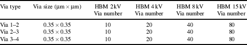
Table 3.2 is an example of the signal pad to ESD clamp wire width requirements based on the wire film layer, and the HBM ESD objective. In technologies, the interconnect film thickness is a function of the wire layer level. In the table, examples of wire layers are chosen from first metal layer, M1, to last metal layer, M4. To maintain the same current density, as the metal layer becomes thinner, the metal wire width must increase accordingly. In addition, as the ESD specification is increased, the wire width must also increase.
Table 3.2 Interconnect wire width requirement vs. HBM ESD objective
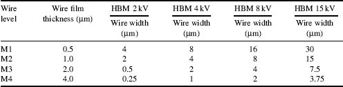
In addition to the metal layer width, the vias between the metal layers must also sustain the ESD event [1, 13–15]. ESD design rule checking and verification are integrated into the ESD design methodologies to ensure adequate via numbers. Table 3.3 is an example of the number of vias required for a given HBM ESD objective. In technologies, the physical size of the vias between metal levels remains the same. For a given ESD specification level, to maintain the same current density, the number of vias between any two metal levels will be constant.
Table 3.3 Via number requirement vs. HBM ESD specification
3.4.2 Interconnect Wire and Via Guidelines for MM ESD Events
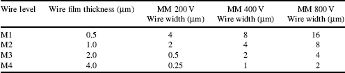
For the MM specification, the peak current is significantly higher than for the HBM. Experimental results of the ESD failure of interconnects for MM show that there is typically a 10: 1 ratio between the HBM and the MM failure levels for interconnects [13, 15]. Table 3.4 shows the interconnect width requirements for MM ESD specification objectives (under the above assumption).
Table 3.4 Interconnect wire width requirement vs. MM ESD objective
3.4.3 Interconnect Wire and Via Guidelines for CDM ESD Events
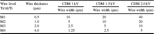
In the CDM specification, a semiconductor chip is charged to a voltage through a high-voltage power supply. The semiconductor chip is discharged by a grounding of a signal pin. Charge throughout the semiconductor chip flows from the VSS power rail, substrate, and VDD power grid to the grounded signal pin. In the CDM event, a rise time on the order of 250 ps occurs, with a high peak current. The CDM event current flows through the power grid, and out through the signal pin wiring. As a result, the power bus (both VSS and VDD) and the interconnect wiring must have high enough cross-sectional area to avoid CDM failures. Table 3.5 provides a table of wire thickness and widths in order to achieve CDM specification objectives. The interconnect is assumed to be a Ti/Al/Ti interconnect structure. CDM events can achieve peak current magnitudes on the order of 10 A.
Table 3.5 Interconnect wire width requirement vs. CDM ESD objective
3.4.4 Interconnect Wire and Via Guidelines for HMM and IEC 61000-4-2 ESD Events
System-level events on external ports can impact semiconductor chips. As a result, system-level designers are requesting the requirement of passing the system-level IEC 61000-4-2 event. The IEC 61000-4-2 specification applies to systems that include non-contact testing. Non-contact testing has two components: the ESD current, as well as the energy associated with the E-field and H-field generated from the discharge event.
A second ESD test specification that only addresses the ESD current of the IEC 61000-4-2 specification is the HMM specification. Both these tests have the same ESD current waveform. The peak current from the IEC 61000-4-2 and HMM test can be on the order of 30 to 40 A of current. As a result, the metal width and via number for the signal pins required to pass this specification are 3× to 4× the requirement needed for CDM testing.
3.4.5 Wire and Via ESD Metrics
This section is on the wire and via ESD metrics for the interconnect and via elements. These are the values for ESD failure of the interconnect or via structure as a function of metal level for the different ESD tests (HBM, MM, and TLP).
Table 3.6 gives the values for ESD failure of the interconnect as a function of metal level for the different ESD tests (HBM, MM, and TLP). These are to be used as “rules of thumb” for wire width design for ESD robustness estimation.
Table 3.6 ESD metrics for wire width for different ESD specifications
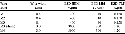
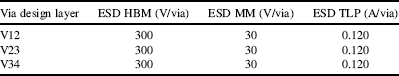
Table 3.7 gives the values for ESD failure of the via structure as a function of metal level for the different ESD tests (HBM, MM, and TLP). These are to be used as “rules of thumb” for ESD robustness estimation.
Table 3.7 ESD metrics for vias for different ESD specifications
ESD power grid resistance is important in the ESD design synthesis. The power grid resistance is critical to the ability of the semiconductor current to discharge the current to the power rail bond pads. As an example, assume a bond pad discharges its current to the ESD alternative current loop through the signal pin ESD device, power bus, and the ESD clamp element between VDD and VSS:
![]()
Then,
![]()
Assuming the ESD network resistance is zero, then we can define a worst case or critical power bus resistance as:
![]()
The critical bus resistance, {Rbus}crit, is the maximum the bus resistance can be prior to failure at the bond pad (see Figure 3.5). The critical voltage, Vcrit, at the bond pad is a function of the circuitry at the signal pin. Note that in this definition, all other resistances in the alternate current loop are regarded as negligible.
Figure 3.5 ESD power grid bus resistance
3.5.1 Power Grid Design – ESD Input to Power Grid Resistance
The design of the interconnects between the ESD network and the power rail can influence the ESD robustness of the semiconductor chip. The current flow from the ESD network to the power rail is important to provide both a low-resistance path and good current distribution. Design symmetry is important in the design to ensure good current distribution through the interconnects. Key design features of the interconnect are as follows:
- Orientation: Broadside orientation of the wire interconnects (e.g., the same direction as the current flow and orthogonal to the stripes).
- Wire Width: Adequate wire width to avoid interconnect failure, degradation, or self-heating.
- Via Number: Adequate via number to avoid via failures, degradation, or self-heating.
- Resistance: Low resistance between the ESD network and the power rail (wiring and vias).
- Wire Design Symmetry: Design symmetry of the wire interconnects from the ESD structure to the power grid.
- Via Design Symmetry: Design symmetry of the via number and placement from the ESD structure to the power grid.
- Segmentation: Segmentation of the wire interconnects to ensure current distribution.
- Comb Design: A wide comb region for the connection between the wire interconnects to the power grid for a low-resistance region across the ESD structure.
Figure 3.6 shows an example of a signal pad, an ESD network, and the wire interconnects between the ESD device and the power rail.
Figure 3.6 Signal pad to ESD signal pad input circuit
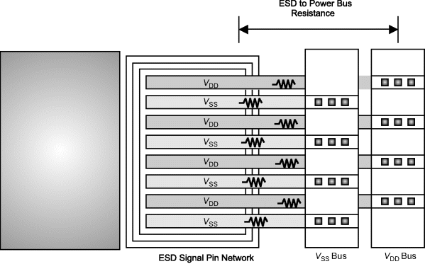
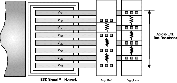
3.5.2 ESD Input to Power Grid Connections – Across ESD Bus Resistance
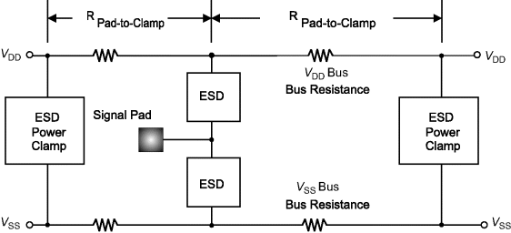
As power bus widths are scaled, the resistance along the bus as it passes through the ESD network can have an influence on the ESD signal pin network operation. In a sub-45 nm technology, in a low pin-count application, the bus resistance across the ESD network can be significant. In the case that the width of the ESD network is on the order of the spacing between an input network and its local ESD power clamp, the resistance across the ESD network can be a large percentage of the ESD bus resistance. Define the parameter “across-ESD bus resistance” as the amount of bus resistance across the signal pin ESD element (Figure 3.7). In the case that the connection of the bond pad ESD to the power bus is perpendicular to the power bus, the ESD current will favor the section of the ESD input network closest to the ESD power clamp. This can lead to premature ESD failure of the signal node and via structures. In a 45 nm application, this leads to ESD failure at 150–175 V MM, and failure of the first via group which has the shortest path to the ESD power clamp. With the reduction of the “across ESD bus resistance,” the ESD results increased to 250 V MM.
Figure 3.7 ESD input circuit to power grid resistance connections – “across ESD” bus resistance
3.5.3 Power Grid Design – ESD Power Clamp to Power Grid Resistance Evaluation
The electrical connections between the ESD power clamp and the power grid are important to ensure proper operation of the ESD power clamp element. ESD power clamps typically contain a trigger element (or network) and a clamping element. The trigger network initiates either the base (in the case of bipolar transistors) or gate (in the case of MOSFET transistors). The clamp element or clamp network provides a “sink” to discharge the ESD current. Figure 3.8 shows the electrical connections between the power bus and the ESD clamp element. Figure 3.9 highlights the resistance in the network. In the implementation, the following features are required for the electrical connection between the power bus and the ESD power clamp:
- Wire Width and Via Number: ESD wire width and via number must be able to support the ESD current magnitude.
- Clamp Element Design Symmetry: Design symmetry is required in the region of the ESD power clamping element to provide uniform current distribution in the clamp element.
- Uniform Resistance and Symmetry: Design symmetry to provide uniform resistance distribution.
- Low-Resistance Connections: Low-resistance connections in series with the ESD clamp elements.
3.5.4 Power Grid Design – Resistance Evaluation
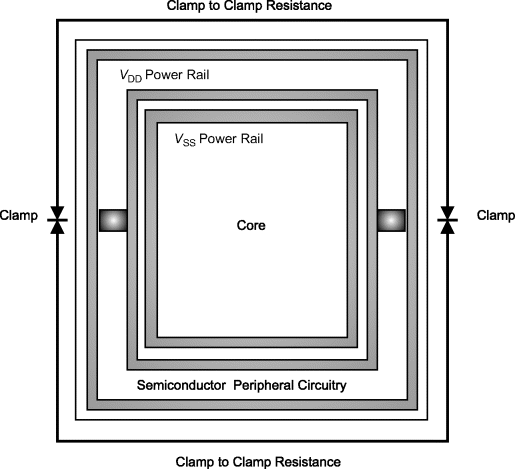
A semiconductor chip, with peripheral I/O circuitry, typically has a peripheral power bus for the networks. Figure 3.10 shows a typical architecture with a VDD power bus, and a VSS power bus. In this architecture, the bus is typically of uniform width around the entire semiconductor chip. A key design parameter is the bus resistance per unit length around the semiconductor chip. A key ESD design metric is the physical resistance along the bus between any signal pin and the ESD power clamp. Figure 3.11 illustrates the resistance between a signal pin and the ESD power clamp. Note in this discussion, only a single distance in one direction is shown.
Figure 3.8 Power grid to ESD power clamp connections
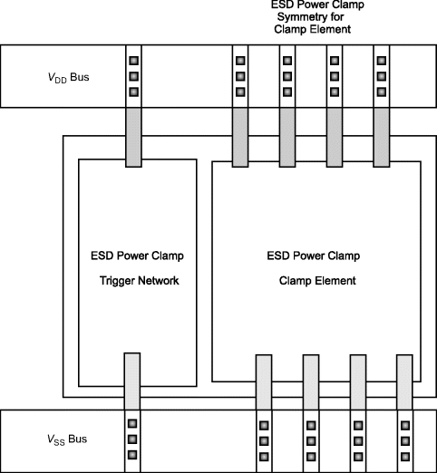
Figure 3.9 ESD power clamp to power grid resistance evaluation
Figure 3.10 Semiconductor chip with a peripheral VDD and VSS power bus
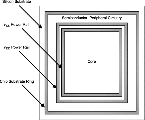
Figure 3.11 Semiconductor floorplan highlighting the signal pin to ESD power clamp distance
This can be represented schematically as shown in Figure 3.12. In this schematic, the key elements are the bond pad, the ESD element, the bus resistance, and the ESD power clamp.
Figure 3.12 Power grid design – resistance evaluation for single current direction current path.
For completeness, in the opposite second direction, there is a second resistance in the power grid.
Figure 3.13 shows an example of the second parallel resistance to the power clamp in the other direction. The two resistance values are in parallel. In this case, the current flows in two directions to the same power clamp or to separate power clamps.
Figure 3.13 Power grid design – resistance evaluation for two parallel paths
3.5.5 Power Grid Design Distribution Representation
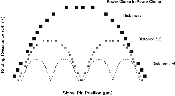
A key parameter in ESD design is the power clamp to power clamp frequency [21]. Figure 3.14 shows a floorplan with a peripheral I/O power bus, where the ESD power clamp to ESD power clamp spacing is highlighted.
Figure 3.14 Power grid design – ESD power clamp to power clamp resistance evaluation
In the ESD design synthesis, the bus resistance between any signal pin to the adjacent power clamp can be plotted [21]. Figure 3.15 shows a routing resistance between any signal pin and the power clamp. In the figure, the first curve is two power clamps. In this case, the worst case pin to power clamp resistance is in the center between the two power clamps. A key ESD design synthesis metric is the worst case resistance between any signal pin and the power clamp. Assume the distance between the two power clamps is L. Hence, the peak of this distribution is the worst case value at position L/2. Adding a third power clamp at position L/2 then reduces the worst case position at L/4 and 3L/4. As extra power clamps are added to the design, the worst case resistance value is reduced.
Figure 3.15 Routing resistance distribution of signal pin to ESD power clamp as a function of pin position
In the power grid design, the width of the power bus is a concern for both chip area and semiconductor processing. In the following sections, a brief discussion of slotting and stacking will be given.
3.6.1 Power Grid Design – Slotting of Power Grid
In semiconductor chip design, the width of metal shapes is limited in the semiconductor process by the technology ground rules. For example, due to chemical mechanical polishing, widths are limited to avoid “dishing” of the metal shapes during the polishing process. As a result, “slots” are formed in the large metal shapes to serve as polishing stops, and lower the effect of dishing. Figure 3.16 shows an example of a power bus highlighting the slots. In the design implementation, the design rule typically states that after a given width, a slot must be formed of a specified width. For example, for every 10 μm of wire width, a slot 1 μm wide may be required to be formed. Hence, for a 20 μm wide power bus, there would be a single slot formed in the center of the power bus.
Figure 3.16 Power grid with slots
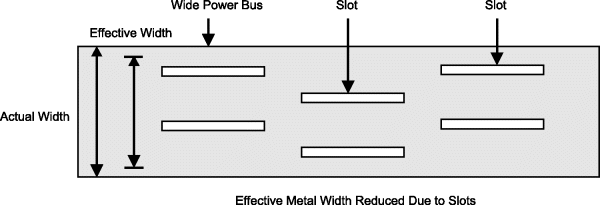
In ESD design synthesis, the power bus resistance is an ESD design rule (e.g., a resistance limit of the power bus between any signal pin and the ESD power clamp). With the placing of slots in the metal width, the effective width, and hence the resistance of the power bus, is impacted. To address this concern, the following can compensate for power bus slotting:
- Width Compensation: Increase the width of the power bus by the amount of width loss due to slotting.
- Effective Width Model: Develop a model to create an “effective width,” where the effective width satisfies the ESD design ground rule for bus width.
- Resistance and Distance Compensation: Decrease the distance between the worst case pin to the nearest ESD power clamp.
3.6.2 Power Grid Design – Segmentation of Power Grids
In semiconductor chip design, the width of metal shapes is limited in the semiconductor process by the technology ground rules [22]. Slots are formed in the large metal shapes to serve as polishing stops, and lower the effect of dishing. Additionally, wide metal shapes can lead to significant inductance in chip design. A method to avoid “slotting” of the metal power bus is segmentation of the power grid into widths below the maximum width rule.
Figure 3.17 shows an example of a power bus highlighting a segmented power rail architecture. One of the advantages of a segmented power rail is for standard cell implementations. In a standard cell, the peripheral cells become narrow and long. The power rails and ground rails must pass through the off-chip driver PFET and NFET, ESD network, and pre-drive circuitry. In order for the power rails to pass through the region of the peripheral rails, the power rail must be segmented into multiple rails.
Figure 3.17 Power grid segmentation
An ESD concern with this concept is that adequate wire width must still be placed in the region of the ESD element for both positive and negative discharging elements. This will become more critical as technologies scale to smaller dimensions [22].
3.6.3 Power Grid Design – Chip Corners
In the ESD design synthesis, the corners of the semiconductor chip are important in the design process. The power grid design in the corners influences both the functional and ESD results by adding resistance to the power grid.
For ESD protection, it is important to have low resistance between the ESD networks at the signal pins and the ESD power clamps placed between VDD and VSS. Current must flow from the ESD signal pin elements, through the VDD power rail, and then the VDD-to-VSS ESD power clamp. The bend at the corners of the power grid can lead to current crowding on the corner, increasing the resistance. When the ESD VDD-to-VSS power clamp is placed around the bend relative to a signal pin prior to the bend, ESD results of different signal pins can be influenced. How this manifests itself is that signal pins on the same side as the ESD VDD-to-VSS power clamp will be higher than signal pins around the bend (e.g., the other edge). Additionally, given there are multiple ESD power clamps on the pad ring, the series resistance of one ESD power clamp will be less than the other, preventing them from responding in parallel. To reduce these effects, there are multiple solutions:
- Additional Edge ESD Power Clamps: Add an additional ESD VDD-to-VSS power clamp on each edge of the semiconductor chip.
- Bend ESD Power Clamps: Place an ESD power clamp on both edges of the bend in the power grid (e.g., two ESD power clamps on the corner on each edge of the bend).
- Bus Chamfered Corners: Chamfer the corner of the power grid to lower the series resistance.
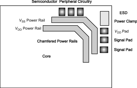
- Wider Bus Corners: Widen the power bus width on the corners.
Figure 3.18 shows the corner region of a semiconductor chip that introduces a chamfered corner to reduce the resistance in the corner region of the power rail. All power rails are chamfered at the corner (e.g., VDD power bus and VSS power bus). Typically, an ESD power clamp is placed in the corner region or inline with the signal pad cells.
Figure 3.18 Power grid design at chip corners
3.6.4 Power Grid Design – Stacking of Metal Levels
In the ESD design synthesis of semiconductor chips, it is important to maintain low resistance between ESD signal pad networks and the power pads as well as to the ESD power clamp.
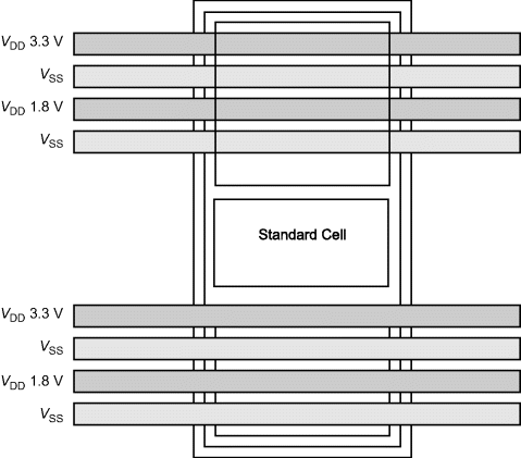
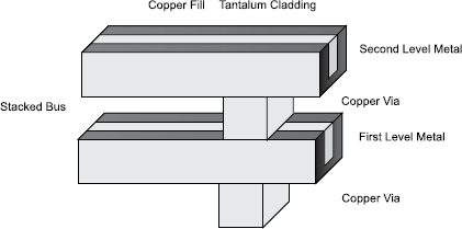
In the architecture of some applications, few metal design layers are used in the design. Additionally, the thinner metal layers are the lowest levels of metal. To maintain low resistance, and reduce chip area, it is necessary to “stack” the metal levels in the power bus.
Figure 3.19 shows an example of a “stacked metal bus” which utilizes multiple metal levels for the power or ground rail. Using multiple metal levels, a low-resistance power bus can be formed without using significant area on the semiconductor chip. Design architectures where this is valuable are the following:
- SRAM Design: SRAM semiconductor chips with peripheral I/O.
- DRAM Design: DRAM semiconductors in the “spine” region.
- Image Processing Design: CMOS image processing chip with peripheral I/O.
3.6.5 Power Grid Design – Wiring Bays and Weaved Power Bus Designs
In chip design synthesis, some regions of the semiconductor chip area are reserved for “wiring bays” for signal lines. An ESD power bus technique is to allow “breaks” in the single or stacked buses to allow passage of the wiring bays. An ESD design synthesis practice is to allow “stitching” around the wiring bays to lower the ESD bus resistance, but allow no interference with the signal passing through the region of the power bus.
Figure 3.19 Power grid stacking of metal levels
3.7 ESD Specification Power Grid Considerations
For special testing or specifications, additional power grid considerations must be addressed. In the next sections, some of the considerations for CDM, IEC 61000-4-2, and HMM specifications will be highlighted.
3.7.1 CDM Specification Power Grid and Interconnect Design Considerations
In the CDM specification, the peak current can exceed 10 A levels. CDM events can lead to failure of power buses, or signal lines, or any interconnect which prevents current flow to the grounded signal pin [22].
In bulk CMOS semiconductor chips, current can flow through the VDD power grid back to the grounded signal pin; in bulk CMOS, current can flow through the entire substrate region as well. The current can flow from the VSS substrate to the VDD power supply through all the well structures. But in SOI technology, the current from the VSS substrate to the VDD power supply can only flow through the interconnects instead of the n-well regions. As a result, the power rails in SOI can fail due to the peak currents during CDM testing; whereas for the identical design in bulk CMOS, no failure occurs in the power grid.
3.7.2 HMM and IEC Specification Power Grid and Interconnect Design Considerations
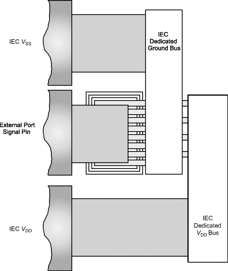
For HMM and IEC 61000-4-2 specifications, the peak current can exceed 30 to 40 A. In the HMM and IEC 61000-4-2 specifications, only pins which are connected to external ports are required to receive this high current pulse. Secondly, the large current in the substrate can influence the non-IEC tested circuitry. To protect the IEC tested pins, and avoid failure of the non-IEC pins, the IEC pins can be isolated in the power grid. This can be achieved by the following means:
- Independent IEC power domain: IEC signal pin, IEC VDD bus, and IEC VSS bus.
- Dual width power bus: IEC and non-IEC domains.
- Resistance Segmentation: Resistance separated IEC and non-IEC domains.
Figures 3.20 and 3.21 show examples of separate IEC vs. non-IEC power grids and connectivity.
Figure 3.20 IEC bus segmentation
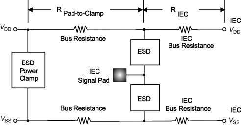
Figure 3.21 IEC bus power and ground placement
3.8 Power Grid Design Synthesis – ESD Design Rule Checking Methods
ESD design rule checking (DRC) and verification methodologies can be used to avoid ESD failures [22–28]. Examples of ESD design synthesis methods will be discussed in this section.
3.8.1 Power Grid Design Synthesis – ESD DRC Methods Using an ESD Virtual Design Level
ESD design checking and verification is performed as part of the ESD design synthesis. A simple methodology can be utilized to verify the metal layer design widths between the signal pad and the ESD, and between the signal pad and the ESD power grid.
An ESD design checking and verification methodology was developed to evaluate the ESD robustness of the interconnects [23]. In this methodology, minimum wire width and maximum resistance constraints are applied to each of the chip's I/O signal pads. These constraints are propagated to the layout design and array pads wired to I/O cells located on the chip. Thus, wiring is such that interconnect wire layers and vias to the ESD protection devices are wide enough to provide adequate ESD protection level. The whole-chip semiconductor design is then verified by first identifying the chip pads, I/O cells, and ESD protection devices. All the electrical connections between these three structures are verified. In this methodology, the power rails are checked between the power rail pads and the ESD power clamps.
The methodology incorporates an “ESD dummy design layer” that identifies the existence of the ESD circuit elements [23]. The virtual ESD dummy layer is placed on the guard ring that surrounds the ESD elements. The methodology utilizes a “shrink” of the wires that are less than the desired ESD metal layer design rules. Wires between the ESD protection devices and the chip pads and I/O cells are shrunk such that unsuitable connections become “opens” (disconnected) and are found in subsequent checking. In this methodology, ESD protection on power lines on integrated chips is verified. The wire and via interconnect ESD protection level between chip pads and an ESD network, between power rails and an ESD network, and on power rails, ground rails, and between power and ground rails.
A method of checking the power grid and electrical connections of an integrated circuit chip for ESD robustness uses the following steps: (1) identify I/O pads on a chip; (2) identify ESD protection devices; (3) represent ESD protection devices as a dummy ESD shape; (4) identify a network comprising wires and vias connecting I/O pads to the ESD dummy shape; (5) determine effective wire cross-sections of the sum of any wires which are connected in parallel to the ESD dummy shape; (6) eliminate connections of vias, wires, and wire cross-sections below a minimum constraint to create “opens”; (7) check for opens to determine I/O pads not connected to the ESD dummy shape; and (8) record any of the said I/O pads not connected to said ESD dummy shape.
The formation of “opens” significantly increases the speed of the ESD design checking system from days to minutes in a large ASIC design. All small interconnect shapes are eliminated below the ESD rule dimensions. Additionally, the ESD virtual shape and the bond pads are saved. In a large ASIC design, this method provides a rapid design rule check and verification of ESD design rule conformance.
3.8.2 Power Grid Design Synthesis – ESD DRC Methods Using an ESD Interconnect Parameterized Cell
In a Cadence™ environment, different techniques can be applied to the ESD design synthesis process. Voldman, Strang, and Jordan developed an ESD methodology incorporating a hierarchical ESD parameterized cell (p-cell) in a foundry environment [24–26]. This concept can be extended by having the power bus and interconnects themselves become a p-cell [28]. In one ESD design methodology, the interconnect is converted into a parameterized cell – a p-cell known as “ESD Interconnect.” In a typical environment, the wiring is not a parameterized cell but by conversion and identification of the power bus and interconnects as “ESD Interconnects,” a checking and verification technique can be applied [28].
As are all circuits, high-level ESD circuits comprise a plurality of lower-level sub-circuits which, in turn, can be expressed in terms of still lower-level elements. The lowest-level ESD elements may be expressed as simple parameterized cells (“p-cells”) – e.g., resistor p-cells, transistor p-cells, varactors p-cells as well as any other basic electronic component. These, in turn, can be used to express higher-level parameterized circuits. These parameterized circuits can, in turn, be connected with parameterized interconnects to ultimately form the ESD circuit. The p-cells exist in a computer aided design (CAD) environment, and are essentially a computer model of the particular element comprising all the parameters necessary for the computer to simulate that element.
In this methodology, by conversion of the interconnect wiring into a parameterized cell itself, the design system provides different means to check and verify the electrical connections. With the introduction of this concept, significant function can be provided to the ESD design synthesis. The ESD design methodology of Voldman, Strang, Collins, and Jordan provides the following concepts [28]:
- A component to verify a connection between a pad and an ESD network by verifying and checking electrical connectivity; a component to verify the width requirements to maintain ESD robustness to a minimum level.
- A component to verify that based on the ESD robustness of the ESD network, the interconnect width and via number are such as to avoid electrical interconnect failure prior to the ESD network failure.
- A component to provide for multiple lines in parallel whose cross-section can be maintained and evaluated as a set of parallel interconnects connected to a single ESD network or plurality of ESD networks.
- A component to provide for “ESD ballasting” by dividing into a plurality of lines.
- A component to provide for calculation of the ESD robustness of the interconnect based on pulse width, surrounding insulator materials (e.g., SiO2 or low K materials), metal level, and distance from the substrate (thermal resistance based on the metal level or underlying structures).
- A component to provide for surrounding fill shapes.
- A component to provide and adjust for “cheesing” of the interconnect.
In this “ESD Interconnect” hierarchical p-cell, the flow of the method establishes the interconnection path of the pad level. Next, an ESD interconnect is verified. The method then verifies an ESD via at the level below. This method is repeated until the lowest level connects to highest metal design level of the input of the ESD network of the corresponding ESD device to that pad. The “ESD Interconnect” can be a single p-cell which contains multiple levels of metal from pad (i) to ESD p-cell (j) where the system verifies the connectivity.
In this method, the ESD interconnect p-cell and algorithm can be established, which prevents the metal level going below a given ESD width. The minimum width can be established by conversion of the metal shape into a p-cell where the metal has an algorithm with a minimum function where the width never goes below a given width defined by the minimum ESD requirement. Checking and verifying that the correct wire width and via number are never below the ESD robustness level of the circuit can be done using the information of the “inherited parameters” contained in the “translation box” formed around the electrical schematic of the hierarchical parameterized cell. The electrical schematic translation box contains the circuit type, the inherited parameters, and pin connections. The translation box may also contain functions – including, for example, ballasting, fill, and cheese. The translation box will allow the transformation of the schematic to the graphical and vice versa. From this, the ESD robustness of the circuit can be determined and stored in the circuit from electrical measurement tables of the design system, as discussed below. Also, from this, the verification that the ESD Interconnect structure p-cell is more ESD robust can be calculated from the ESD robustness wire calculations.
By way of illustration, ESD robustness of an interconnect can be calculated based on the metal level and effective metal width. For example, for a given technology file, the metal film thicknesses and materials are known. In this fashion, from the design level, and the technology file, and experimental data, a table is constructed. Also in this fashion, a “lookup table” is constructed which is based on design data and experimental results – the size of the interconnect can be judged as achieving the ESD objective. In the GUI, the input variable can choose an ESD model such as HBM. Once the GUI choice is made, the ESD HBM level can then be chosen. For example, if the GUI input is that the HBM level is to be greater than 4000 V, then all interconnects from the pad must be auto-generated to increase to a minimum width.
For the case of copper interconnects, the HBM ESD robustness level is 2× the aluminum level for the same thickness.
In the case of the MM, ESD robustness levels are 5× to 10× lower. In this fashion, in a “lookup table” which is based on design data and experimental results, the size of the interconnect can be judged as achieving the ESD objective. In the GUI, the input variable can choose an ESD model such as MM. Once the GUI choice is made, the ESD MM level can then be chosen.
In the case that multiple models, such as HBM, MM, and CDM, levels are required, the design system can be established so that the metal line width is such that all models achieve the desired levels and the minimum thickness is chosen so that all models are satisfied [28].
Analytical models, such as those developed by Wunsch–Bell or Smith–Littau, can be utilized for prediction of the critical current or power to failure. Analytical models can be used which require the heat capacity, the thermal conductivity, the melting temperature, and the pulse width of the event instead of empirical look-up tables. In this fashion, the GUI would either store the material properties and/or allow user-defined properties that are required for the analytical equation. Using the analytical models, material properties of the metal wire and the insulator properties can be used which will allow predictive capability for a given ESD event. The metal line would then be auto-generated to guarantee non-failure to that ESD event of a given current level, voltage level, or pulse width [28].
In the case of filling, the fill shapes change the effective thermal conductivity of the insulator. This can be handled in the analytical models by modifying the effective thermal conductivity of the surrounding medium. In the case of “cheesing,” holes are formed in the metal. In this case, the metal width must be increased to allow for the total cross-sectional area the same.
In the case of ballasting, the metal line can be separated into a plurality of parallel wires where the wire widths are such that the total width is equal to the calculated width based on the analytical model or the lookup table result. Ballasting can be an option or a requirement of a design, or implementation.
Plurality of parallel lines and ESD ballasting needs can also be addressed by the ESD Interconnect p-cell. In the case where it is a requirement that interconnect ballasting of the ESD device is a critical need, a check can be performed where the lowest level of metal of the ESD Interconnect p-cell is divided into a plurality of interconnects which integrates with the ESD network.
If the ESD network translation box contains information that ESD ballasting is required for that specific design, the check then verifies that the ESD interconnect also contains this requirement or design failure is stated. Hence, an ESD Interconnect p-cell can have as a parameter the formation of a plurality of interconnects, and also verifies that this feature is “checked” relative to the ESD network translation box information of the ESD p-cell for the highest level of the p-cell and the lowest level of the ESD Interconnect p-cell.
To verify the presence of ESD power clamps between two power rails, the checking system provides a verification step where the labeled power pads are also connected such that the ESD Interconnect p-cell is utilized for the power grid, and an ESD power clamp. The verification and checking system will check:
- ESD Interconnect: The presence of the ESD Interconnect p-cell.
- ESD Power Pad to ESD Interconnect: The interconnection between the power pad and the ESD Interconnect p-cell.
- ESD Power Clamp: The presence of an ESD power clamp.
- ESD Power Clamp Type: The type of the ESD power clamp.
- ESD Power Clamp Size: The size of the ESD power clamp.
In this case, the verification and checking system will verify:
- The “connectivity” from power pad, ESD interconnect;
- ESD power clamp; and
- ESD interconnect and a power ground pad.
Between two ground power rails, or a common potential of two separated power supplies, the verification and checking of the ESD rail-to-rail device can be verified against its ESD Interconnect connection. ESD ballasting, ESD robustness, and inherited parameters can be contained in the translation box and stored for cross-comparison between the pads, the interconnect, and the ESD network [28].
3.9 Summary and Closing Comments
In this chapter, the discussion has continued to address issues associated with full-chip ESD design synthesis. The chapter focuses on the interconnects and power grid layout and design itself, and addresses interconnect robustness, interconnect failure, and key metrics in the whole-chip ESD design synthesis. With an understanding of the inter-relationship between the power grid and the ESD networks, full-chip integration can be addressed. With our “top-down” approach, it is possible to focus on what kind of circuits are placed in the power grid. This leads us into the next chapter.
In Chapter 4, the discussion focuses on ESD power clamp networks. A key issue in ESD design synthesis is the type of ESD network used in the power grid domain. This was discussed briefly in previous chapters, but the whole of Chapter 4 will be dedicated to ESD power clamp discussions.
Problems
3.1. Assuming a peripheral pad architecture, a chip is formed with I/O and bond pads on the periphery. Draw a semiconductor chip that has dimensions w and l. Assume the bond pads for the circuits are wBP and lBP, with spacing wsp and lsp between bond pads. Assume an ESD power clamp is placed on the corners of a chip. Assuming a bus width of WBUS for a single material ρ, of thickness t, derive an equation for resistance as a function of pin location on the chip, addressing only the resistance in one direction. Assume the ESD device connection to the power bus is in the center of the I/O cell (bond pad).
3.2. Assuming there are two corners with ESD power clamps, derive an equation for two resistance values from any signal pin to the power clamps (e.g., derive an equation from any signal pin position between the two power clamps). Plot the total resistance as a function of pin position. Assume the ESD device connection to the power bus is in the center of the I/O cell (bond pad position).
3.3. In a semiconductor chip, interconnect scaling theory assumes the metal film thickness scales as a MOSFET constant electric field scaling parameter, α. For each layer, the film scales thinner. Derive the relationship of Problems 3.1 and 3.2, assuming for each layer the film thickness increases as t′ = tα. Assume N layers of metal.
3.4. In semiconductor technology, interconnects are both copper and aluminum. Show the equations of Problems 3.1 and 3.2 assuming that the material type and thickness change, based on whether it is aluminum or copper. Derive the relationship with a ratio parameter of sheet resistance ρAl/ρCu and film thickness parameters.
3.5. In semiconductor technology, with the introduction of slotting, large rectangular slots are formed in the power bus, of dimensions wslot and lslot. Assume slots are formed of pitch p in the width of the bus W. Derive the resistance relationship as a function of the width of the bus. Hint: Show the stepwise relationship. Derive the bus resistance relationship of Problems 3.1 and 3.2.
3.6. In semiconductor technology, with the introduction of copper interconnects, for polishing purposes, the wire interconnects are required to have shapes removed in the metal as a function of the width. Derive a relationship that has, when a metal bus exceeds a dimension WWM, a “cheese” width WCHEESE is removed (for each multiple of dimension WWM). Given a bus of width w, show the relationship for width graphically, addressing the “cheesing.” Derive the resistance relationship as a function of the width of the bus. Hint: Show the stepwise relationship. Note, assume cheesing in the length dimension follows the same relationship and cheese shapes are square.
3.7. Assume an ESD network has a width the same as the bond pad. Assume an ESD network is segmented into N parallel connection wires from the ESD network to the power rail. Assume the individual connections are of ESD wire width, WESD. Show the resistor ladder network formed between the ESD element and the power bus (e.g., include the resistance of the bus, WBUS, of a single material ρ, of thickness t).
3.8. As the power bus scales in advanced technologies, the bus resistance is significant within the ESD network, leading to non-uniform ESD operation. Assume the ESD power clamp is N bond pads away. What is the percentage of the power rail resistance within the ESD network as a function of the distance of the power clamp? Show it as a function of the number of pads from the power clamp.
3.9. As in Problem 3.8, the “across ESD resistance” can be a significant part of the bus resistance. Derive a relationship for “across ESD resistance” based on the bus width parameter, the bond pad dimension, the wire interconnect width, the number of vias between the ESD and the power bus. Assume an ESD network has a width the same as the bond pad. Assume an ESD network is segmented into N parallel connection wires from the ESD network to the power rail. Assume the individual connections are of ESD wire width, WESD. Show the resistor ladder network formed between the ESD element and the power bus (e.g., include the resistance of the bus, WBUS, of a single material ρ, of thickness t).
3.10. To reduce the bus resistance, stacking of metal films in parallel is done in many semiconductor chips in peripheral I/O design. Derive a relationship for the bus resistance as a function of the width, length, and MOSFET constant electric field scaling parameter, α. (e.g., the film thickness increases as t′ = tα). Assume two metal levels that are one layer from each other (e.g., M1 and M2). Assume the general case of any two layers. Assume the case of any two design layers.
1. S. Voldman. ESD: Physics and Devices, Chichester, UK: John Wiley and Sons, Ltd, 2004.
2. S. Voldman. ESD: Circuits and Devices, Chichester, UK: John Wiley and Sons, Ltd, 2006.
3. S. Voldman. ESD: Failure Mechanisms and Models, Chichester, UK: John Wiley and Sons, Ltd, 2009.
4. D.C. Wunsch and R.R. Bell. Determination of threshold failure levels of semiconductor diodes and transistors due to pulsed voltages, IEEE Transactions on Nuclear Science, NS-15, (6), December 1968; 244–259.
5. D. Tasca. Pulse power modes in semiconductors. IEEE Transactions on Nuclear Science, NS-17, (6), 1970; 364–372.
6. J. Smith. Electrical overstress failure analysis in microcircuits. Proceedings of the Electrical Overstress/Electrostatic Discharge (EOS/ESD) Symposium, 1981; 41– 46.
7. J. Smith and W. Littau. Prediction of thin film resistor burnout. Proceedings of the Electrical Overstress/Electrostatic Discharge (EOS/ESD) Symposium, 1981; 192– 197.
8. D. Egelkrout. Metallization failure and thermo-mechanical shock studies, Boeing Corporation, Defense Atomic Support Agency Report 2611 (SRD), November 1971.
9. E. Kinsbron, C.M. Melliar-Smith, and A.T. English. Failure of small thin film conductors due to high current density pulses. IEEE Transactions on Electron Devices, ED-26, (1) 1979; 22–26.
10. D. Pierce. Modeling metallization burnout of integrated circuits. Proceedings of the Electrical Overstress/Electrostatic Discharge (EOS/ESD) Symposium, 1982; 56– 61.
11. T. Maloney. Integrated circuit metal in the charged device model: Bootstrap heating, melt damage, and scaling laws. Proceedings of the Electrical Overstress/Electrostatic Discharge (EOS/ESD) Symposium, 1992; 129– 134.
12. K. Banerjee, A. Amerasekera, and C.M. Hu. Characterization of VLSI circuit interconnect heating and failure under ESD conditions. Proceedings of the IEEE International Reliability Physics Symposium (IRPS), 1996; 237– 245.
13. S. Voldman. ESD robustness and scaling implications of aluminum and copper interconnects in advanced semiconductor technology. Proceedings of the Electrical Overstress/Electrostatic Discharge (EOS/ESD) Symposium, 1997; 316– 329.
14. S. Voldman. High-current transmission line pulse characterization of aluminum and copper interconnects for advanced CMOS semiconductor technologies. Proceedings of the IEEE International Reliability Physics Symposium (IRPS), 1998; 293– 301.
15. S. Voldman. The impact of technology evolution and scaling on electrostatic discharge (ESD) protection on high-pin-count high-performance microprocessors. Proceedings of the International Solid-State Circuits Conference (ISSCC), Session WA21, San Francisco, CA, February 15–17, 1999; 366– 367.
16. K. Banerjee, A. Amerasekera, G. Dixit, and C.M. Hu. The effect of interconnect scaling and low-K dielectric on the thermal characteristics of the IC metal. International Electron Devices Meeting (IEDM) Technical Digest, December 1996; 65–68.
17. S. Voldman. High current characterization of dual damascene copper/SiO2 and low-K inter-level dielectrics for advanced CMOS semiconductor technologies. Proceedings of the IEEE International Reliability Physics Symposium (IRPS), 1999; 144– 153.
18. K. Banerjee, D.Y. Kim, A. Amerasekera, C.M. Hu, S.S. Wong and K.E. Goodson. Microanalysis of VLSI interconnect failure modes under short-pulse stress conditions. Proceedings of the IEEE International Reliability Physics Symposium (IRPS), 2000; 283– 288.
19. S. Khoo, P. Y. Tan, and S. Voldman. Microanalysis and electro-migration reliability performance of transmission line pulse (TLP) stressed copper interconnects. Journal of Microelectronics and Reliability, 2003; 43: 1039–1045.
20. L. Chu, W. K. Chim, K.L. Pey, and A. See. Effect of transmission line pulsing of interconnects investigated using combined low-frequency noise and resistance measurements. Proceedings of the International Physical and Failure Analysis (IPFA) Symposium, 2001; 97– 102.
21. P. A. Juliano and W. Anderson. ESD protection design challenges for a high pin-count Alpha microprocessor in a 0.13 μm CMOS SOI technology. Proceedings of the Electrical Overstress/Electrostatic Discharge (EOS/ESD) Symposium, 2003; 59– 69.
22. C. J. Brennan, J. Sloan, and D. Picozzi. CDM failure modes in a 130 nm ASIC technology. Proceedings of the Electrical Overstress/Electrostatic Discharge (EOS/ESD) Symposium, 2004; 182– 186.
23. R. Bass, D. Nickel, D. Sullivan, and S. Voldman. Method of automated ESD protection level verification. U.S. Patent No. 6086627 July 11th 2000.
24. S. Voldman, S. Strang, and D. Jordan. An automated electrostatic discharge computer-aided design system with the incorporation of hierarchical parametrized cells in BiCMOS analog and RF technologies for mixed signal applications. Proceedings of the Electrical Overstress/Electrostatic Discharge (EOS/ESD) Symposium, 2002; 296– 305.
25. S. Voldman, S. Strang, and D. Jordan. A design system for auto-generation of ESD circuits. Proceedings of the International Cadence Users Group, September 2002.
26. S. Voldman. Automated hierarchical parameterized ESD network design and checking system. U.S. Patent No. 6,704,179 March 9th 2004.
27. P. Homsiger, A. Huber, D. Korejwa, W. Livingstone, J. Panner, E. Schanzenbach, D. Stout, S. Voldman, and P. Zuchowski. Method of automated design and checking for ESD robustness. U.S. Patent No. 6,725,439, April 20th 2004.
28. D. Collins, D. Jordan, S. Strang, and S. Voldman. ESD design, verification, and checking system and method of use. U.S. Patent No. 7,134,099, November 7th, 2006.