Chapter 7
ESD Full-Chip Design Integration and Architecture
7.1 Design Synthesis and Integration
ESD protection is fundamental to semiconductor chip design [1–5]. In this chapter, examples of ESD design synthesis and integration will be discussed for different chip designs. The chapter will begin by discussing architectures for memory [6–21], microprocessors [22–42], ASIC standard cell [43–49], analog and radio frequency [50–59]. The sections will provide examples of digital, analog, RF, mixed-signal, and mixed-voltage interface chip integration and architectures.
ESD design synthesis in digital design typically does not require co-synthesis of the ESD solutions and the digital circuitry for digital design applications below 1 GHz [1–49]. But, the ESD design synthesis must be integrated into the floorplan of a semiconductor chip.
Integration of the ESD networks is built into the architecture of the chip to ensure achieving ESD protection for all pin combinations specified in the ESD standards. ESD protection must be provided between signal pins and power rails, power rail-to-power rails, and pin-to-pin. In semiconductor designs, circuitry interfacing with other semiconductor chips or systems can be at the same voltage or different voltage levels. Peripheral circuits and power rails are separated from internal core circuitry and other sensitive functions. Guard rings are placed to minimize interaction and injection between the different chip domains. To address these considerations, the semiconductor design synthesis must have the following:
- Full-chip guard ring.
- Separate power rails for different power domains.
- ESD networks within each domain.
- ESD networks between each chip domain.
7.3 Custom Design vs. Standard Cell Design
In semiconductor chip design, ESD design synthesis is a function of whether the design is custom [1–42], or in a standard cell architecture [43–49]. In custom design, the floorplan engineer has the freedom to place different domains in different locations in the semiconductor chip. Power bus placement and ESD can be placed as desired within the ESD design rules, and design manual rules for the technology. ESD designs can be customized to the area or region for optimized placement. ESD designs can be pre-established, parameterized cells, or customized design layers.
In a standard cell design integration, specific rules are established for placement of the bond pads, peripheral circuits, power bus, ground bus, guard rings, and ESD elements. In a standard cell design methodology, ESD designs are integrated with the standard cell circuitry. ESD input and output circuitry are placed in the standard cell footprint. ESD power clamps are also pre-defined for the customer. With this architecture, only limited changes in the design can be integrated.
In this section, ESD design synthesis for different memory architectures will be shown as examples.
7.4.1 DRAM Design
ESD protection and design synthesis is challenging in dynamic read access memory (DRAM) [6–15]. Area and capacitance loading of ESD networks are severe constraints on the high-speed memory input receiver networks. Additionally, advanced DRAMs are typically the first product in a technology generation, leading to new ESD concerns and learning in a new technology. To add to this, the native voltage of the DRAM is lower than the products it is interfacing with; this requires mixed-voltage interface (MVI) circuitry that must drive higher voltages.
In a DRAM design floorplan, the memory arrays are segmented into bits of DRAM cells, bit lines, word lines, and sense amplifier logic. All other functions are contained within a given region of the semiconductor chip. There are three architecture floorplans:
- Peripheral Exterior: Bond pads and I/O on the periphery of the semiconductor chip.
- Vertical Spine: Bond pads and I/O in the symmetrical center in the long dimension of the semiconductor chip (e.g., height).
- Horizontal Spine: Bond pads and I/O in the symmetrical center in the short dimension of the semiconductor chip (e.g., width).
For floorplans with peripheral I/O, the bond pad, power rails, and ESD placement are similar to many other standard products. In this case, the edges of the I/O bond pads have a short wire bond length to the package pins. The peripheral I/Os are separated from the DRAM arrays with a guard ring, so I/O circuitry and ESD circuitry does not interfere with the DRAM cells.
For the other cases, with a vertical or horizontal “spine,” the configuration is significantly different. The “spine” is the section of the DRAM that contains the bond pads, I/O circuitry, and ESD networks. In this region, the I/O circuit power bus and I/O ground are defined. The area constraints used for the spine are limited to avoid wasting too much area for non-memory function. In the spine region, there exist the following:
- Bond pads.
- VDD (I/O) power rail.
- VSS (I/O) power rail.
- VDD core power rail.
- VSS substrate power rail.
- Voltage regulators VDD (I/O) to VDD (core).
- I/O circuitry.
- ESD signal pin ESD networks.
- ESD VDD (I/O) to VSS (I/O) networks.
- ESD VSS (I/O) to VSS networks.
- Decoupling capacitors.
Figure 7.1 shows an example of a DRAM chip floorplan with a vertical spine. A vertical spine was required in a 4 Mb DRAM.
Figure 7.1 DRAM design with a vertical spine

Figure 7.2 shows an example of a DRAM chip floorplan with a horizontal spine. A horizontal spine was utilized in a 16 Mb DRAM [6–8].
Figure 7.2 DRAM design with a horizontal spine
In the case of an internal spine, the package must interface with the internal bond pads. One method to interconnect the package to the internal spine is using a “transfer wire,” which is a thick layer that is part of the packaging and molding process. The transfer wire is connected to a short wire bond between the transfer wire and the internal bond pads.
Some of the challenges in ESD are as follows:
- Mixed-voltage interface I/O circuits.
- Multiple power rails (e.g., VDD (I/O), VDD, VSS (I/O), and VSS).
- Low-capacitance external power rail (e.g., VDD (I/O)).
- Regulated core VDD.
- Limited area in the spine region.
Mixed-voltage interface circuits: To address the mixed-voltage interface concern, OCDs introduce resistors in series with the NFET transistors. Typically, no integrated ballast resistors are used to save space. Using an independent resistor element is more efficient from an area perspective. Using the PFET drain-to-n-well diode, this assists in providing good ESD protection with a reduced area for the ESD element.
Multiple-power ESD signal pin networks: Unique ESD networks are used at the bond pad that have direct current paths to three or four rails [7, 11]. These “three-rail” ESD networks can provide a forward-biased diode discharge path to VDD (I/O), VSS (I/O), and VSS. These have been utilized from 16 Mb to 1 Gb DRAM chips. Figure 7.3 shows an example of a three-rail ESD network [11, 12].
Figure 7.3 DRAM ESD network with three rails
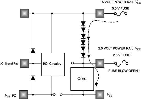
ESD regulator bypass network: In DRAMs, the voltage regulator is a p-channel transistor whose well and source are connected to the VDD (I/O) rail (Figure 7.4). As a result, no current flows from the I/O power rail to the regulated VDD core power rail. In early DRAM development, an ESD regulator bypass network was used in parallel with the regulator to allow the ESD current flow to the high-capacitance rail of the semiconductor chip [13]. An n-channel MOSFET was distributed along the length of the spine, where the n-channel gate and source was connected to VDD, and whose drain was connected to VDD (I/O).
Figure 7.4 ESD regulator bypass circuitry integration
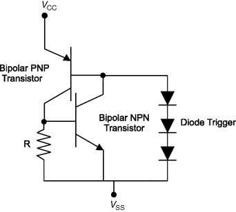
ESD VDD(I/O) power clamp: In advanced technology, concerns over the discharge into the core memory led to not adding an ESD regulator bypass. As a result, a local ESD power clamp was added between the VDD (I/O) rail and VSS (I/O) (or directly to VSS). In advanced 1 Gb DRAMs, a DTSCR was used for the ESD power clamp [14, 15]. The disadvantage of this method is the limited area for external ESD power clamps, as well as not taking advantage of the natural capacitance and size of the DRAM chip. Figure 7.5 shows an example of a DTSCR.
Figure 7.5 1 Gb DRAM diode-triggered SCR for ESD VDD-to-VSS power clamp
With technology scaling, one of the challenges of the ESD design is in the spine region. With the scaling of the bond pad size, and power buses, it is more difficult to achieve HBM, MM, and CDM results in the advanced DRAM products. But still today, 2000 V HBM, 200 V MM, and 1000 V CDM are achievable with 1–2 Gb DRAM products in 45 nm technology [5].
7.4.2 SRAM Design
In a static read-access memory (SRAM) design, the architecture is established to provide the highest utilization for the memory array, and the highest speed [17–20]. ESD design synthesis of a SRAM design typically requires peripheral pad design. The floorplan contains all the bond pads on the periphery of the semiconductor chip, away from the core SRAM cell arrays (Figure 7.6). For speed, it is advantageous to have the OCD circuitry on the periphery with the bond pad, power rails, and ESD network. To provide fast memory, it is an advantage to have the receiver networks in the interior of the core region.
Figure 7.6 SRAM design floorplan

As an example of a SRAM ESD architecture, the receiver networks were such that the bond pad and primary ESD network were on the periphery of the chip, but the receiver itself was on the interior of the design.
On the periphery, ESD p + /n-well diodes and n-well to substrate diodes were used between the power rail and ground. The core capacitance was large, so no additional ESD power clamps were used. ESD HBM results exceeded 5 kV HBM [18].
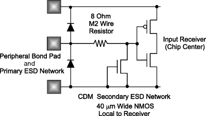
Figure 7.7 shows the ESD circuitry for the SRAM design. A wide interconnect extended from the periphery to the interior, forming an 8Ω resistor in series with the receiver. Since the placement of the receiver network was a significant distance from the periphery, a secondary stage CDM network was placed local to the receiver. The interconnect wire was utilized as a CDM resistor; no additional resistor element placed in series. A 40 μm wide grounded-gate n-channel MOSFET was placed near the receiver inverter network. CDM test simulation results showed that without the CDM MOSFET near the receiver, the CDM results were 200 V CDM. With the CDM MOSFET, the CDM results exceeded 1200 V.
Figure 7.7 SRAM design ESD circuitry
This implementation demonstrates the following ESD design synthesis concepts:
- Usage of peripheral ESD networks on the exterior of the semiconductor chip.
- Utilization of a secondary ESD CDM stage placed local to the inverter receiver.
- Utilization of the natural resistance of the wire interconnect from the exterior of the chip to the internal receiver for CDM protection.
7.4.3 Non-Volatile RAM ESD Design
In non-volatile RAM (NVRAM) applications, semiconductor chips may have a 3.3 V native power rail, a 5 V power rail, and a 12 V programming pin for the NVRAM circuitry. Some of the unique issues with the NVRAM ESD protection are as follows:
- Program Pin Latchup: 12 V power pin can lead to CMOS latchup and electrical overstress.
- Programming Flash-Induced Injection: Programming flash can lead to photon-induced leakage events in functional circuits and ESD networks.
Programming pins can lead to injection of minority carriers. Programming pins must be sufficiently isolated and have guard rings that satisfy high-voltage circuit solutions. Forward biasing of ESD elements, electrical overstress, and mis-sequencing is an issue with the programming pin.
In a NVRAM technology, the MOSFET gate oxide can use a dual-gate thin oxide [21]. Figure 7.8 shows a sequence-independent ESD network using a triple-oxide p-channel MOSFET. The ESD network has a p-channel MOSFET as a “well bias control”; a lateral pnp is contained within the well. In one aspect, there is a dual-oxide ESD protective network for non-volatile memory in which ESD protection is provided using a thick oxide PFET in a thick epitaxial layer with sequence-independent circuitry. The dual-oxide gate of the p-channel MOSFET is connected to the 12 V input programming node, the source is connected to the 5 V power rail, and the drain is connected to its own n-well region. When the programming pin is low, the p-channel MOSFET is “on” and the n-well is biased at 5 V. When the programming pin is high (e.g., 12 V), the n-well floats. This provides ESD protection and avoids electrical overstress.
Figure 7.8 NVRAM chip design

The dual-oxide ESD network includes a high-voltage PFET ESD network for 12 V to 5 V applications, as well as a low-voltage PFET network for 5 V to 3 V applications taking advantage of dual oxides supported by the disclosed technology. The circuit saves space, is migratable, improves reliability, and is voltage differential independent.
In a microprocessor, the architecture and chip size are important for both microprocessor performance, yield, and net profits. Microprocessors utilize advanced CMOS technology [22–24]. Additionally, SOI technology is used for mainstream microprocessor development [38–42]. In 25-wafer lots of microprocessors, each lot can be worth millions of US dollars. Significant focus in a microprocessor is on the placement of the cache, and other critical circuitry that optimizes the chip performance metrics.
7.5.1 3.3 V Microprocessor with 5.0 V to 3.3 V Interface
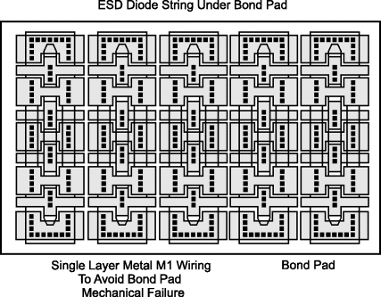
As an example of one microprocessor architecture, in a 0.35 μm channel length technology, a PowerPC microprocessor was constructed with 140 MHz performance [30–35]. The area needed for ESD protection represented 8% of the entire chip area. It was decided – for chip size, performance, and net cost – to place the ESD circuitry under the bond wire pads (Figure 7.9). The bond pad size, at this technology node, was 130 μm × 130 μm. The microprocessor had a 3.3 V power supply, and needed to interface with 5 V. The floorplan contained all the bond pads on the periphery of the semiconductor chip. The package was a quad flat pack (QFP) package.
Figure 7.9 ESD under bond pad chip design – five diode string
The off-chip driver was a mixed-voltage interface circuit containing an n-channel MOSFET series cascode pull-down, and a “floating well” p-channel pull-up. For the mixed-voltage interface, the ESD design needed to be compatible with the I/O bi-directional circuit.
The ESD design chosen was a series of p + /n-well diodes between the signal pads and the 3.3 V to receive a 5 V signal. On the periphery, five ESD p + /n-well diodes and n-well to substrate diodes were used between the power rail and ground. The core capacitance was so significant that no additional ESD power clamps were used. Since no other circuits were allowed under the bond pads except diode networks, the ESD network filled the area under the bond wire pads. The ESD network was placed adjacent to the bi-directional off-chip driver signal pins. With the spatial placement of the ESD network local to the bi-directional OCD, no additional CDM secondary network was needed for CDM protection.
A first concern was the design of the metal layer pattern under the wire bond pad. In the ESD design layout synthesis, different metal patterns were used to verify the integrity of the bond pad after the bond pad stress test.
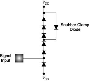
A second concern was with the implementation of five p + /n-well diodes in series; a parasitic bipolar Darlington effect was discovered due to the common collector parasitic pnp transistors. This common collector amplification of the leakage was eliminated by a “snubber diode” [30–32]. Figure 7.10 shows the ESD network with the “snubber diode” to eliminate the Darlington amplification.
Figure 7.10 ESD schematic with snubber diode element
ESD results of the CPU design (after optimization of the perimeter of the diodes) of 8000 V HBM were achieved after two successive microprocessor design passes. Perimeter-to-area optimization of the STI p–n diodes increased the HBM ESD results from 800 V to 8000 V with no change in the size of the ESD network [30–32].
This implementation demonstrates the following ESD design synthesis concepts:
- ESD Under Bond Pads: Usage of peripheral ESD networks under bond wire pads.
- Metal Pattern Optimization: Optimization of metal wire pattern under bond pad was required to avoid insulator cracking and bond pad integrity.
- Mixed-Voltage Interface ESD: Utilization of a mixed-voltage interface ESD network.
- Darlington Effect: Elimination of the parasitic Darlington effect in the ESD network using a snubber diode between successive diode elements.
- ESD Diode Perimeter-to-Area Optimization: Perimeter-to-area optimization can lead to significant increase in the ESD robustness of a semiconductor product with no process or area increase of the ESD design.
7.5.2 2.5 V Microprocessor with 5.0 V to 2.5 V Interface
The first 2.5 V power supply microprocessor was required to interface with 5.0 V power supply semiconductor chips [3, 5]. The first 2.5 V power supply PowerPC chip, at 100 MHz, replaced a 5 V/3.3 V 33 MHz microprocessor. This implementation was the first 0.25 μm CMOS technology in the semiconductor industry. This microprocessor integrated two power supply rails in the design; an external power rail at 5 V, and an internal core native power supply voltage at 2.5 V power supply (Figure 7.11). For the external I/O circuitry, the circuitry must receive and drive 5 V signals. The input circuitry contained an n-channel half-pass transistor to lower the voltage on the MOSFET gate of the receiver. The n-channel MOSFET half-pass transistor was followed by a BR element and grounded-gate MOSFET prior to the input gates.
Figure 7.11 5 V to 2.5 V CMOS microprocessor architecture
An ESD network connected a p–n diode between the signal pad and the 5 V power supply pin. A “diode string” of seven p–n diodes was placed between the 5 V power rail and the 2.5 V power rail [3, 5]. In this time period, no ESD power clamps were placed between the VDD and the VSS power rail. The ESD event was distributed to the 2.5 V power rail, and the native capacitance of the chip was used to discharge the current to the ground plane.
7.5.3 1.8 V Microprocessor with 3.3 V to 1.8 V Interface
In the next technology node, another microprocessor chose to place the OCDs in the interior of the microprocessor. The OCDs were formed in OCD banks, where each grouping contained a service module. The service module contained power and the ESD power clamps for the set of local off-chip drivers. Eight I/Os were placed in each OCD bank, and these OCD banks were strategically placed for both performance and packaging considerations. To allow for sequence independence between the 3.3 V power rail and a 1.8 V power rail, a sequence-independent ESD network was utilized; this allowed for each power rail to be brought up independently without forward biasing of an ESD network. The sequence-independent network used a lateral pnp element in a “floating well”; the floating well was biased by a floating well control network using a p-channel MOSFET [11, 12].
With technology scaling, as the power supply differential voltages were reduced, the number of elements between the power supplies was reduced. At the same time, there was an increase in the need for independence of the power supply rails. In this period, innovation introduced different circuits to allow this to occur. The design practice also eventually introduced ESD power clamps between the VDD and VSS power rails, eliminating the VDD-to-VDD ESD networks in most applications; this avoided sequencing issues between power rails, improved the domain-to-domain isolation, and at the same time eliminated redundancy of current paths.
7.6 Application-Specific Integrated Circuits
In this section, ESD implementation and design synthesis in ASIC applications will be discussed.
7.6.1 ASIC ESD Design
Application specific IC (ASIC) design synthesis must incorporate the ESD design synthesis in the formation of the methodology from the first definition of the “ASIC methodology” [44]. In an ASIC methodology, the floorplan and the ASIC “rule set” are integrated for customer usage. The ASIC methodology must be a co-synthesis with the ESD design process. The ASIC method that influences ESD must incorporate the following:
- Power rail placement.
- Power rail bus widths.
- Bond pad width and spacing (pitch).
- Standard cell form factor (width and height).
- Power bond pad placement and “power book.”
- Signal pin bond pad placement and standard cell.
- Input placement of I/O standard cells.
- Power rail placement over the I/O standard cells.
- Signal pin standard cell percentage of area for ESD networks.
- Signal pin standard cell guard rings.
- Power pad standard cell ESD networks.
In the ASIC methodology, all these design variables must be established to define the ESD implementation [48].
In a full ASIC methodology, there may be as many as 400–500 different I/O standard cells. These I/O standard cells contain different receiver and off-chip circuitry.
7.6.2 ASIC Design Gate Array Standard Cell I/O
In the ASIC design methodology, the functional and ESD requirements must be co-synthesized. With a large number of standard cells, methods are needed to reduce the number of circuits using creative methods, rules, and CAD techniques. In a standard cell design integration, specific rules are established for placement of the bond pads, peripheral circuits, power bus, ground bus, guard rings, and ESD elements. In a standard cell design methodology, ESD designs are integrated with the standard cell circuitry. ESD input and output circuitry is placed in the standard cell footprint. ESD power clamps are also pre-defined for the customer. With this architecture, only limited changes in the design can be integrated.
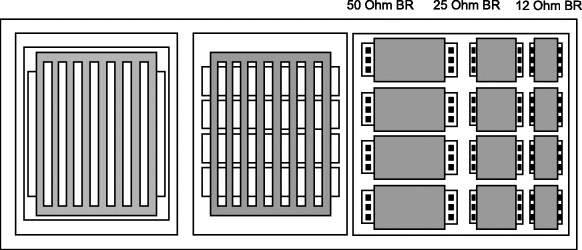
In one methodology, to provide different standard cell impedance, resistors are formed in a “gate array” method. In this methodology, the same standard cell can be used for different OCD strengths. These resistor elements serve as both series resistors for the correct series impedance and ballasting resistor.
Figure 7.12 shows an example of a standard cell with an array of different resistors. One set is used for each different desired impedance. The unused resistors are “grounded” and the row of incorporated resistors wired in series with the MOSFET OCD. This methodology was incorporated into a 0.35 μm CMOS technology generation. In the integration of the different circuits, each case of the circuit is tested and verified for functionality and ESD protection levels.
Figure 7.12 ASIC chip design with resistor “bank” for different I/O OCD strength
7.6.3 ASIC Design System with Multiple Power Rails
In an ASIC system, multiple power supplies are needed due to mixed-voltage environments. ESD protection must exist in ASIC standard cells, and as part of the ASIC architecture. Sequence independence between power rails is key to avoid limiting customers to sequencing requirements.
A novel ESD protection circuit for multiple power supplies, having both inventive inter-rail ESD circuitry and inventive single-rail ESD circuitry, was implemented by D.W. Stout, S. Voldman, J. Sloan, J. Pequignot, and T. Rahman [45]. The inter-rail ESD circuitry is scalable and comprises one or more diode strings for interconnecting a pair of power rails. The ESD trigger voltage for a diode string is set by the number of diodes within the diode string and preferably a sufficient number of diodes are provided within each diode string for power-up and power-down sequence independence. The single-rail ESD circuitry is connected to a level-shifter and may comprise an RC discriminator comprising two NFET transistors connected in series. The RC discriminator may be connected to a clamping transistor via a buffering circuit, such as an inverter stage, that isolates the gate capacitance of the clamping transistor from the RC discriminator so that the RC characteristics of the RC discriminator are unaffected by the choice of the clamping transistor. The ESD protection circuit may be constructed from a selection of user-selectable discrete circuit elements formed on the chip [45–47].
7.6.4 ASIC Design System with Voltage Islands
In advanced technologies, power consumption is a large concern in big semiconductor chips and systems. Power management techniques were incorporated into microprocessors to reduce the power consumption.
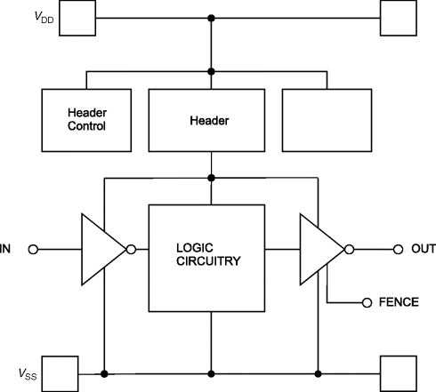
In an ASIC environment, a concept known as “voltage islands” is used to reduce power consumption. Figure 7.13 shows an example of a voltage island. In a voltage island, an independent power domain is established internally by forming a “dummy bus” within the voltage island. The voltage island incorporates a “header,” a “header control,” a dummy power bus, and a “fence.” In this implementation, what distinguishes this concept from microprocessors is that in this method, some signals are still “powered” whereas all other circuits within the “voltage island” are shut down. In the past, microprocessors may have powered down completed chip sectors; in this method, some signals remain powered.
Figure 7.13 ASIC chip design with voltage islands
The ESD and latchup issues influenced are as follows:
- Segmentation of the power grid into separated domains from the VDD through header and header controls.
- Placement of active circuit-powered networks adjacent to shut-down networks.
Many customers or corporations have different preferences in the ESD power clamp design. One “gate array” ESD power clamp concept is to have a standard cell which contains a plethora of elements for the design team to construct their own RC-triggered ESD power clamp. Figure 7.14 shows an example of a “ESD gate array kit” for design teams to develop their own design [46, 47]. The kit would contain a multi-finger MOSFET, inverters, resistors, and capacitor arrays. This concept was proposed by S. Voldman and J. Pequignot for ASIC development. In this fashion, the customer can provide his own design synthesis within the parameters and models of a given standard cell environment. This is a method for automatically generating a custom ESD network for an integrated circuit. When a user provides chip size and chip capacitance for the integrated circuit, components for the customized ESD network are automatically selected based on the user-provided chip size and chip capacitance, and the adequacy of the ESD behavior of an ESD network employing the selected components is evaluated.
Figure 7.14 ASIC gate array ESD design

An ASIC book comprising a gate-array format of ESD components is provided. A customized, optimized, and tuned ESD network can be constructed from the ASIC book. Novel ESD circuitry having inter-rail ESD circuitry and single-rail ESD circuitry can be constructed. The inter-rail ESD circuitry is scalable and comprises one or more diode strings for interconnecting a pair of power rails. The ESD trigger voltage for a diode string is set by the number of diodes within the customized diode string, and preferably a sufficient number of diodes are provided within each diode string for power-up and power-down sequence independence. The single-rail ESD circuitry is connected to a level-shifter and may comprise an RC discriminator comprising a customizable plurality of NFET transistors connected in series. The RC discriminator may be connected to a clamping transistor via a buffering circuit, such as an inverter stage, that isolates the gate capacitance of the clamping transistor from the RC discriminator. In a second aspect of the invention, an ASIC book comprising a gate-array format of ESD components is provided. A customized, optimized, and tuned ESD network can be constructed from the ASIC book.
7.7 CMOS Image Processing Chip Design
Image processing chips have seen considerable growth in the last few years, with the usage of digital cameras and cell phones. Image processing chips are used in digital cameras, where both high-quality images and low power consumption are important. Noise and power are important to utilize these chips in digital cameras, where battery life limitations are a concern. CMOS imaging chips are advantageous over CCD chips due to low power consumption, making it ideal for battery power applications. Additionally, it does not introduce “blooming.” CMOS image processing chips can incorporate analog-to-digital converters (A/DC) for direct digital output.
Small imaging device are also used in cellular phones. Specifically, solid state imaging devices are needed that can achieve high levels of micro-miniaturization, low cost, and high performance.
A metric for an image processing semiconductor array is the number of pixels and pixel densities. It is desirable to have the size of the imaging array as large as possible. For example a CMOS sensor may have a 1.3 Mega-pixel imaging array with 1280 × 1024 resolution. As a result, semiconductor imaging chips have large “core” area, and are “core-limited” design architectures. The imaging area must also be free of circuits to allow capturing of the image through the entire physical area. To achieve this, the digital logic circuits, I/O and ESD networks must exist on the periphery of the semiconductor image processing chip.
In a “core-limited” ESD design synthesis for CMOS imaging chips, the architecture contains the following:
- Peripheral power rails.
- Peripheral ground rails.
- Peripheral bond pads.
- Many power domains for isolation (e.g., 8 power domains).
- Breaker cells between the power domains.
- ESD power clamps between each power and ground domain.
- ESD VSS-to-VSS cells between the ground power rails.
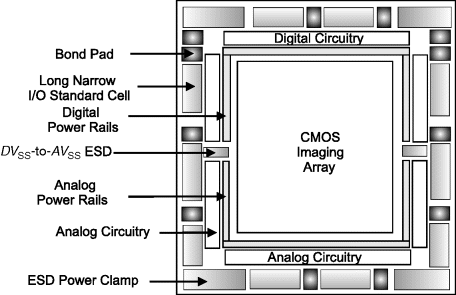
A unique feature of the CMOS image processing chips is that the area on the periphery is large, and the pin count is low for the size of the chip. A CMOS image chip may be as large as a large ASIC design, but may have less than 50 pins (e.g., 48-pin package). In a standard ASIC cell system, the design is “pad-limited” with long/narrow standard cells on the periphery. In a CMOS image processing chip core-limited design, the spacing between signal pads is large, allowing for a large number of ESD resources. In these designs, foundry long/narrow standard cells would waste significant area. The solution for this is a foundry cell known as a short/wide standard cell, or rotation of the long/narrow standard cells perpendicular to the normal orientation.
7.7.1 CMOS Image Processing Chip Design with Long/Narrow Standard Cell
Figure 7.15 shows a CMOS image processing chip using a long/narrow I/O standard cell. The standard cell is rotated relative to the normal orientation of the design. This then requires additional connections to the power bus, which is parallel to the long dimension of the long/narrow I/O cell. ESD power clamps must also be rotated since, in a standard cell library, these also conform to the same form factor as the standard cell itself.
Figure 7.15 CMOS image processing chip design with long/narrow I/O
7.7.2 CMOS Image Processing Chip Design with Short/Wide Standard Cell
Figure 7.16 shows a CMOS image processing chip with the short/wide I/O standard cell, and a short/wide ESD power clamp. In this case, the peripheral area is better utilized. In these image processing chips, significant area is available to add ESD power clamps and breaker cells between the power domains. In a CMOS image processing chip, there are a significant number of separated power domains due to the noise considerations. A second key consideration for the number of ESD power clamps is the total chip IDD leakage current. In the chip design synthesis, the total chip IDD leakage specification is significantly lower than an ASIC-type application. As a result, consideration of the leakage on the VDD is a major ESD design limitation for the number of ESD power clamps utilized in the design (not the silicon area).
Figure 7.16 CMOS image processing chip design with short/narrow I/O standard cells

In an MS architecture, digital, analog, and RF circuitry can be contained on the same semiconductor chip. In the following sections, chip design synthesis and ESD issues will be discussed.
7.8.1 Mixed-Signal Architecture – Digital and Analog
In an MS architecture, the digital and analog circuitry is separated into different power domains. Analog design requires unique layout and design characteristics [50–53]. Power electronics also require unique layout, design, and guard ring requirements [54, 55]. Figure 7.17 shows an example of a semiconductor chip with digital and analog domains. To avoid ESD failures in an MS semiconductor chip, ESD protection networks are placed between the analog ground (AVSS) and the digital ground (VSS). Typical architectures contain a separate ESD power clamp in each domain. An ESD power clamp exists in the digital domain, between VDD and VSS, and a second ESD power clamp exists in the analog domain, between analog VDD (AVDD) and analog ground (AVSS).
Figure 7.17 Mixed-signal architecture – digital and analog architecture

7.8.2 Mixed-Signal Architecture – Digital, Analog, and RF
In an MS architecture, the digital, analog, and RF circuitry is separated into different power domains. Radio frequency ESD design synthesis differs significantly from both analog and digital design [56–59]. To avoid ESD failures in an MS semiconductor chip, ESD protection networks are placed between the analog ground (AVSS), the digital ground (VSS), and the RF ground. Typical architectures contain a separate ESD power clamp in each domain. An ESD power clamp exists in the digital domain, between VDD and VSS; a second ESD power clamp exists in the analog domain, between analog VDD (AVDD) and analog ground (AVSS); and a third ESD power clamp exists between RF VDD (RFVDD, or VCC) and RF ground (RFVSS, or VEE). In these mixed-signal chips, the RF application voltage is typically higher than the analog and digital application voltage.
Figure 7.18 shows an example of a mixed-signal chip with RF, analog, and digital circuitry. To separate the analog circuitry from the digital noise, separate power rail domains exist. Additionally, a guard ring “moat” separates the two domains to produce a larger distance through the substrate region. The RF sector is separated on the lower sector of the chip floorplan. ESD network power clamps are placed in the digital, analog, and RF domains between their power and ground rails. In addition, VSS-to-VSS ESD networks are placed to interconnect the ground rails. The VSS-to-VSS networks use series diode ESD elements, where the number of elements in series is a function of the allowed capacitive coupling between the digital, analog, and RF sectors.
Figure 7.18 Placement and mixed-signal architecture – digital, analog, and RF architecture

The RF circuitry is surrounded by layers of metal forming a “faraday cage” to isolate the RF signals. The faraday cage is formed by stacking the metal layers, and passing the signals through the breaks in the faraday cage. An example of the RF faraday cage is shown in Figure 7.19. Interconnect layers and via groups are stacked from the silicon substrate to the upper-level metal. In the substrate, the faraday cage is electrically connected to the substrate region with heavily doped layers. Signal lines are passed from the analog and digital domains through the faraday cage to reach the RF circuitry. This prevents electromagnetic interference (EMI) from the digital and analog domains affecting the RF circuitry.
Figure 7.19 RF faraday cage in a mixed-signal architecture – digital, analog, and RF design

The RF sector has a VCC and VSS power rail dedicated to RF circuitry. ESD power clamps are placed between the VCC and VSS of the RF domain. ESD power clamps consist of RF components to allow for RF modeling and tracking. ESD networks can be constructed from the RF circuit elements. The circuits are dependent if the technology is RF CMOS, or RF BiCMOS. In an RF CMOS application, the ESD power clamps can be RC-triggered MOSFET ESD power clamps [56–58]. In a BiCMOS technology, the ESD power clamps can be constructed of bipolar transistors [56–58].
7.9 Summary and Closing Comments
In this chapter, the focus has been on examples of design synthesis in full-chip implementations. Examples of DRAM, SRAM, microprocessors, mixed-voltage, mixed-signal, and RF applications were shown. As part of the ESD design synthesis, the layout is key to a successful design implementation for both ESD and CMOS latchup. These examples will provide some understanding of the challenges in the ESD full-chip integration issues. By combining the knowledge of Chapters 1, 2, 3, 4, 5, 6 with this chapter, the whole chip design strategy should be better understood for any semiconductor chip architecture.
Problems
7.1. In early DRAM applications, the ESD alternate current path was to discharge the ESD current into the array, with no exterior rail power clamps. A CMOS DRAM chip is formed with trench DRAM cells. The DRAM array consists of DRAM capacitors of 100 fF per trench DRAM cell. Estimate the DRAM capacitance of the array for 1 Mb to 4 Gb DRAM, assuming the DRAM cell size remains the same. Show a DRAM ESD architecture that allows for current discharge to the array core. Assume an independent peripheral power and ground and regulated DRAM core array.
7.2. In early microprocessors, no ESD power clamps were used in the peripheral area or in the core of the CPU. Estimate the capacitance of a digital microprocessor, assuming 50% of the area was an n-well region on a p-/p + + wafer in a 10 mm × 20 mm chip. Given the frequency of the HBM pulse, what is the impedance (e.g., Z = |1/ω C|)? Given an ESD power clamp was added in parallel with the core capacitance, how low must the series resistance be in order to be effective? Compare with the chip core capacitance.
7.3. A semiconductor chip is charged during CDM testing. Assume a semiconductor chip is 100% digital logic circuits. Plot the chip capacitance between VDD and VSS as the chip size is increased from 1 mm × 1 mm to 20 mm × 20 mm. Assume an n-well to substrate capacitance value. What is the total charge stored in the chip? Assume the chip is discharged in 1 ns, what is the magnitude of the current as a function of chip size?
7.4. In semiconductor chip design, empty areas are “filled” with “fill shapes” for photo, etch, and chemical mechanical polishing (CMP) uniformity. What is the effect of fill shapes in the metal levels when an ESD current pulse is sent through a signal line interconnect surrounded by fill shapes? What is the electrical and thermal influence? If the fill shapes are placed in an array, how does this affect the electrical and thermal profile in the wire interconnect?
7.5. In semiconductor chip design, empty areas are “filled” with “fill shapes” for photo, etch, and CMP uniformity. In some applications, instead of fill shapes, de-coupling capacitors are added near the peripheral I/O areas. The decoupling capacitors can consist of an n-well lower plate that is grounded, and a MOSFET gate structure on the n-well region. Decoupling capacitors are formed by placement of an n-channel MOSFET in an n-well. What is the impact of the de-coupling capacitors when placed between I/O networks? What is the potential concern of placement near p-channel MOSFET driver circuits? What is the impact of the de-coupling capacitors if placed near ESD input circuits? What are the advantages and disadvantages?
7.6. Show the ESD architecture of a semiconductor chip with a digital and analog core. Place back-to-back diodes between the two core sectors on the grounds. Assume a pin-to-pin ESD test is performed between an analog and digital pin. Show the bi-directional current path.
7.7. A mixed-signal chip has a digital core and an analog core. A signal line exists between the two core regions, where a digital driver sends the signal to a receiver in the analog sector. Given an aluminum wire width of 1 μm, and wire film thickness of 1 μm, calculate the resistance from the digital core driver to the receiver assuming the signal is sent from across half of the semiconductor chip size, where the chip size increases from 2 mm × 2 mm to 20 mm × 20 mm. Assume a current of 1 mA in the interconnect, what is the voltage drop across the wire?
7.8. Show the ESD architecture of a semiconductor chip with a digital and analog core. A signal line exists between the two core regions, where a digital driver sends the signal to a receiver in the analog sector. Place back-to-back diodes between the two core sectors on the grounds. Assume an ESD current flows through the signal line. Show the possible current path. Show the maximum number of diodes and voltage across the signal line.
7.9. Show the ESD architecture of a semiconductor chip with a digital and analog core. A signal line exists between the two core regions, where a digital driver sends the signal to a receiver in the analog sector. Place cross-domain ESD networks from the digital VDD to the analog VSS. Also show back-to-back diodes between the two core sectors on the grounds. Assume an ESD current flows through the signal line. Show the possible current paths.
7.10. In an image processing chip, the total IDD current specification is low to avoid impact on the power application. Assume an IDD specification of 100 μA. In the chip, the leakage sources on the VDD power rail are the array, the logic, and the ESD power clamps. What ESD networks provide low leakage? How many are needed to protect an image processing chip? What type of ESD networks are not suitable?
1. A. Amerasekera and C. Duvvury. ESD in Silicon Integrated Circuits. Chichester, UK: John Wiley and Sons, Ltd, 1995.
2. S. Voldman. ESD: Physics and Devices. Chichester, UK: John Wiley and Sons, Ltd, 2004.
3. S. Voldman. ESD: Circuits and Devices. Chichester, UK: John Wiley and Sons, Ltd, 2005.
4. S. Dabral and T. J. Maloney. Basic I/O and ESD. New York: John Wiley and Sons, Inc., 1998.
5. S. Voldman. ESD: Failure Mechanisms and Models. Chichester, UK: John Wiley and Sons, Ltd., 2009.
6. E. Adler, J. K. DeBrosse, S. F. Geissler, S. J. Holmes, M. D. Jaffe, J. B. Johnson, C. W. Koburger, J. B. Lasky, B. Lloyd, G. L. Miles, J. S. Nakos, W. P. Noble Jr., S. H. Voldman, M. Armacost, and R. Ferguson. The evolution of IBM CMOS DRAM technology. IBM Journal of Research and Development, 39 (1–2), Jan/March 1995; 167–188.
7. S. Voldman, V. Gross, M. Hargrove, J. Never, J. Slinkman, M. O'Boyle, T. Scott, and J. Delecki. Shallow trench isolation (STI) double-diode electrostatic discharge (ESD) circuit and interaction with DRAM circuitry. Proceedings of the Electrical Overstress/Electrostatic Discharge (EOS/ESD) Symposium, 1992; 277– 288.
8. S. Voldman, V. Gross, M. Hargrove, J. Never, J. Slinkman, M. O'Boyle, T. Scott, and J. Delecki. Shallow trench isolation (STI) double-diode electrostatic discharge (ESD) circuit and interaction with DRAM circuitry. Journal of Electrostatics, 31 (2–3), 1993; 237–265.
9. S. Voldman and V. Gross. Scaling, optimization, and design considerations of electrostatic discharge protection circuits in CMOS technology. Proceedings of the Electrical Overstress/Electrostatic Discharge (EOS/ESD) Symposium, 1993; 251– 260.
10. S. Voldman and V. Gross. Scaling, optimization, and design considerations of electrostatic discharge protection circuits in CMOS technology. Journal of Electrostatics, 33 (3), October 1994; 327–357.
11. S. Voldman. ESD protection in a mixed voltage interface and multi-rail disconnected power grid environment in 0.5- and 0.25-μm channel length CMOS technologies, Proceedings of the Electrical Overstress/Electrostatic Discharge (EOS/ESD) Symposium, 1994; 125– 134.
12. S. Voldman. Electrostatic discharge protection circuits for mixed voltage interface and multi-rail disconnected power grid applications. U.S. Patent No. 5,945,713, August 13, 1999.
13. S. Voldman. Voltage regulator bypass circuit. U.S. Patent No. 5,625,280. April 29, 1997.
14. S. L. Jang, M. S. Gau, and C. K. Lin. Novel diode-chain triggering SCR circuits for ESD protection. Solid State Electronics, 44, 2000; 1297–1303.
15. M. Mergens, C. Russ, K. Verhaege, J. Armer, P. Jozwiak, R. Mohn, B. Keppens, and S. Trinh. Diode triggered SCR (DTSCR) for RF ESD protection of BiCMOS SiGe HBT's and CMOS ultra-thin gates oxides. International Electron Device Meeting (IEDM) Technical Digest, 2003; 515–518.
16. S. Voldman. The impact of MOSFET technology evolution and scaling on electrostatic discharge protection. Review Paper, Microelectronics Reliability, 38, 1998; 1649–1668.
17. R. D. Adams, R. C. Flaker, K. S. Gray, H. L. Kalter. An 11ns 8K x 18 CMOS static RAM. Proceedings of the International Solid State Circuits Conference (ISSCC), 1988; 242– 243.
18. H. Pilo and S. Lamphier. A 300 MHz, 3.3 V 1 Mb SRAM fabricated in a 0.5 μm. CMOS process, Proceedings of the International Solid State Circuits Conference (ISSCC), February 1996; 148– 149.
19. H. S. Lee, B. El Kareh, R. C. Flaker, G. G. Gravenities, R. A. Lipa, J. P. Maslack, J. R. Pessetto, W. F. Pokorny, M. A. Roberge, T. Williams, H. A. Zeller, and K. E. Beilstein. An experimental 1Mb CMOS SRAM with configurable organization and operation. Proceedings of the International Solid State Circuits Conference (ISSCC), 1988; 180– 181.
20. H. Pilo, A. Allen, J. Covino, P. R. Hansen, S. Lamphier, C. Murphy, T. Traver, P. Yee. An 833-MHz 1.5 W 18-Mb CMOS SRAM with 1.67 Gb/s/pin. IEEE Journal of Solid State Circuits, Vol. 35, Issue 11, November 2000; 1641–1647.
21. R. E. Rose, R. C. Szafranski, and S. Voldman. Dual thin oxide ESD network for nonvolatile memory applications. U.S. Patent No. 5,872378, February 16, 1999.
22. C. W. Koburger, W. F. Clark, J. W. Adkisson, E. Adler, P. E. Bakeman, A. S. Bergendahl, A. B. Botula, W. Chang, B. Davari, J. H. Givens, H. H. Hansen, S. J. Holmes, D. V. Horak, C. H. Lam, J. B. Lasky, S. E. Luce, R. W. Mann, G. L. Miles, J. S. Nakos, E. J. Nowak, G. Shahidi, Y. Taur, S. H. Voldman, F. R. White, and M. R. Wordeman. A half-micron CMOS logic generation. IBM Journal of Research and Development, 39 (1/2), Jan/March 1995; 215–228.
23. G. G. Shahidi, J. D. Warnock, J. Comfort, S. Fischer, P. A. McFarland, A. Acovic, T. I. Chappell, B. A. Chappell, T. H. Ning, C. J. Anderson, R. H. Dennard, J. Y.-C. Sun, M. R. Polcari, and B. Davari. CMOS scaling in the 0.1 1.X-volt regime for high performance applications. IBM Journal of Research and Development, 39 (1/2), Jan/March 1995; 229–244.
24. Y. Taur, Y. J. Mii, D. J. Frank, H. S. Wong, D. A. Buchanan, S. J. Wind, S. A. Rishton, G. A. Sai-Halasz, and E. J. Nowak. CMOS scaling into the 21st century: 0.1 μm and beyond. IBM Journal of Research and Development, 39 (1/2), Jan/March 1995; 245–260.
25. S. Voldman. The impact of technology evolution and scaling on electrostatic discharge (ESD) protection in high pin count high performance microprocessors. Invited Talk, Proceedings of the International Solid State Circuits Conference (ISSCC), Session 21, WA 21.4, 1999; 366– 367.
26. S. Voldman, W. Anderson, R. Ashton, M. Chaine, C. Duvvury, T. Maloney, and E. Worley. Test structures for benchmarking the electrostatic discharge (ESD) robustness of CMOS technologies. SEMATECH Technology Transfer Document, SEMATECH TT 98013452A-TR, May 1998.
27. S. Voldman, W. Anderson, R. Ashton, M. Chaine, C. Duvvury, T. Maloney, and E. Worley. ESD technology benchmarking strategy for evaluation of the ESD robustness of CMOS semiconductor technologies. Proceedings of the International Reliability Workshop (IRW), 1998; October 12– 16.
28. S. Voldman, W. Anderson, R. Ashton, M. Chaine, C. Duvvury, T. Maloney, and E. Worley. A strategy for characterization and evaluation of the ESD robustness of CMOS semiconductor technologies. Proceedings of the Electrical Overstress/Electrostatic Discharge (EOS/ESD) Symposium, 1999; 212– 224.
29. S. Voldman. Electrostatic discharge protection, scaling, and ion implantation in advanced semiconductor technologies. Invited Talk, Proceedings of the Ion Implantation Conference (I2CON), Napa, California, 1999.
30. S. Voldman and G. Gerosa. Mixed voltage interface ESD protection circuits for advanced microprocessors in shallow trench and LOCOS isolation CMOS technology, International Electron Device Meeting (IEDM) Technical Digest, December 1994, 811–815.
31. S. Voldman, G. Gerosa, V. Gross, N. Dickson, S. Furkay, and J. Slinkman. Analysis of snubber-clamped diode string mixed voltage interface ESD protection networks for advanced microprocessors, Proceedings of the Electrical Overstress/Electrostatic Discharge (EOS/ESD) Symposium, 1995; 43– 61.
32. S. Voldman, G. Gerosa, V. Gross, N. Dickson, S. Furkay, and J. Slinkman. Analysis of snubber-clamped diode string mixed voltage interface ESD protection networks for advanced microprocessors, Journal of Electrostatics, 38 (1–2), October 1996; 3–32.
33. R. Countryman, G. Gerosa, and H. Mendez. Electrostatic discharge protection device. U. S. Paten No. 5,514,892, May 7, 1996.
34. S. Voldman. Optimization of MeV retrograde wells for advanced logic and microprocessor/PowerPC and electrostatic discharge (ESD). Invited Talk, Smart and Economic Device and Process Designs for ULSI Using MeV Implant Technology Seminar: SEMICON West, SEMICON West GENUS Seminar, San Francisco, 1994.
35. G. Gerosa, M. Alexander, J. Alvarez, C. Croxton, M. D'Addeo, A. R. Kennedy, C. Nicoletta, J. P. Nissen, R. Philip, P. Reed, H. Sanchez, S. A. Taylor, and B. Burgess. A 250-MHz 5-W PowerPC microprocessor with on-chip L2 cache controller. IEEE Journal of Solid-State Circuits, 32 (11), Nov. 1997; 1635–1649.
36. S. Dabral, R. Aslett, and T. Maloney. Designing on-chip power supply coupling diodes for ESD protection and noise immunity. Proceedings of the Electrical Overstress/Electrostatic Discharge (EOS/ESD) Symposium, 1993; 239– 249.
37. S. Dabral, R. Aslett, and T. Maloney. Core clamps for low voltage technologies. Proceedings of the Electrical Overstress/Electrostatic Discharge (EOS/ESD) Symposium, 1994; 141– 149.
38. S. Voldman, R. Schulz, J. Howard, V. Gross, S. Wu, A. Yapsir, D. Sadana, H. Hovel, J. Walker, F. Assaderaghi, B. Chen, J. Y. C. Sun, and G. Shahidi. CMOS-on-SOI ESD protection networks. Proceedings of the Electrical Overstress/Electrostatic Discharge (EOS/ESD) Symposium, 1996; 291– 302.
39. S. Voldman, F. Assaderaghi, J. Mandelman, L. Hsu, and G. Shahidi. Dynamic threshold body- and gate-coupled SOI ESD protection networks. Proceedings of the Electrical Overstress/Electrostatic Discharge (EOS/ESD) Symposium, 1997; 210– 220.
40. S. Voldman, D. Hui, L. Warriner, D. Young, R. Williams, J. Howard, V. Gross, W. Rausch, E. Leobangdung, M. Sherony, N. Rohrer, C. Akrout, F. Assaderaghi, and G. Shahidi. Electrostatic discharge protection in silicon on insulator (SOI) technology. Invited Talk, Proceedings of the IEEE International SOI Conference Symposium, Session 5.1, 1999; 68– 72.
41. S. Voldman, D. Hui, D. Young, R. Williams, D. Dreps, M. Sherony, F. Assaderaghi, and G. Shahidi. Electrostatic discharge (ESD) protection in silicon-on-insulator (SOI) CMOS technology with aluminum and copper interconnects in advanced microprocessor semiconductor chips. Proceedings of the Electrical Overstress/Electrostatic Discharge (EOS/ESD) Symposium, 1999; 105– 115.
42. P. A. Juliano and W. R. Anderson. ESD protection design challenges for a high pin-count Alpha microprocessor in a 0.13 μm CMOS SOI technology Proceedings of the Electrical Overstress/Electrostatic Discharge (EOS/ESD) Symposium, 2003; 59– 69.
43. S. Voldman. Power sequence independent electrostatic discharge protection circuits U.S. Patent No. 5,610,791, March 11, 1997.
44. J. H. Panner, T. R. Bednar, P. H. Buffet, D. W. Kemerer, D. W. Stout, P. S. Zuchowski. The first copper ASICs: A 12M-gate technology. Proceedings of the IEEE Custom Integrated Circuits Conference (CICC), 1999; 347– 350.
45. J. Pequignot, T. Rahman, J. H. Sloan, D. W. Stout, and S. Voldman. Method and apparatus for providing ESD protection. U.S. Patent No. 6,157,530, December 5, 2000.
46. J. Pequignot, T. Rahman, J. H. Sloan, D. W. Stout, and S. Voldman. Method for providing ESD protection for an integrated circuit. U.S. Patent No. 6,262,873, July 17, 2001.
47. J. Pequignot, T. Rahman, J. H. Sloan, D. W. Stout, and S. Voldman. ASIC book to provide ESD protection on an integrated circuit. U.S. Patent No. 6,292,343, September 18, 2001.
48. C. J. Brennan, J. Sloan, and D. Picozzi. CDM failure modes in 130 nm ASIC technology. Proceedings of the Electrical Overstress/Electrostatic Discharge (EOS/ESD) Symposium, 2004; 182– 186.
49. J. Pequignot, J. Sloan, D. Stout, and S. Voldman. Electrostatic discharge protection networks for triple well semiconductor devices. U.S. Patent Application 7,348,657, July 15, 2004.
50. P. Gray, Hurst, Lewis, and Meyer. Analysis and Design of Analog Integrated Circuits. 5th Edition. New York: John Wiley and Sons, Inc., 2009.
51. W. M. C. Sansen. Analog Design Essentials. Springer, Netherlands, 2006.
52. A. Hastings. The Art of Analog Layout. 2nd Edition. New Jersey: Pearson Prentice Hall, 2006.
53. V. A. Vashchenko and A. Shibkov. ESD Design in Analog Design, New York: Springer, 2010.
54. B. J. Baliga. High Voltage Integrated Circuits. IEEE Press, New York, 1988.
55. P. Antognetti. Power Integrated Circuits: Physics, Design, and Applications. McGraw-Hill, New York, McGraw-Hill, 1986.
56. S. Voldman. The state of the art of electrostatic discharge protection: physics, technology, circuits, designs, simulation and scaling. Invited Talk. Bipolar/BiCMOS Circuits and Technology Meeting (BCTM) Symposium, 1998; 19–31.
57. S. Voldman. A review of latchup and electrostatic discharge (ESD) protection in BiCMOS RF silicon germanium technologies: Part I – ESD. Microelectronics and Reliability 2005, 45; 323–343.
58. S. Voldman. ESD: RF Technology and Circuits. Chichester, UK: John Wiley and Sons, Ltd, 2006.
59. P. Leroux and M. Steyaert. LNA-ESD Co-design for Fully Integrated CMOS Wireless Receivers. New York: Springer: 2005.