Chapter 4
ESD Power Clamps
In this chapter, ESD power clamp networks will be explored. ESD power clamp usage began in the mid-1990s, and today is a common practice of semiconductor chip design and ESD design synthesis [1–52]. Development of ESD power clamps and the synthesis into the semiconductor chip architecture is part of the ESD design discipline and an essential component of the art of ESD design. This chapter will focus on the classification of the ESD power clamps, key design parameters, the ESD power clamp design window, trigger elements, clamp devices, and issues and problems with the ESD power clamp.
4.1.1 Classification of ESD Power Clamps
There are many different types of ESD power clamps, but conceptually they can be classified into different categories. Figure 4.1 shows a diagram of classification of ESD power clamps.
Figure 4.1 Classes of ESD power clamps
ESD power clamps must be tolerant of the power supply voltages observed in the functional semiconductor chip or system of chips [3–6]. ESD power clamps can be constructed for the native voltage power supply or mixed voltage power supplies. The ESD power clamps must be tolerant of the semiconductor chips they interface with, or the number of power rail voltages contained within a given chip.
Fundamentally, ESD power clamps contain some basic features. A first feature is the transfer of ESD current from one segment of the power grid to a second segment of the power grid. A second feature is the initiation of the ESD power clamp, commonly referred to as a “trigger” state. ESD power clamps can be as simple as one physical device or a complex circuit, or a system. In the simplest case, the trigger feature and the clamp feature can be contained within the same device. In a second classification, the trigger element is independent of the “clamp” feature (e.g., independent trigger element from the clamping feature). There is a critical concept in the ESD power clamp design synthesis in the separation of the trigger state feature from the clamp feature. The advantage of an independent trigger element is that it provides a second degree of freedom with the separation of the clamping feature from the trigger feature. Whereas with a single integrated element, there is a physical limitation on some devices to achieve the features desired.
In a third classification, the ESD power clamp is a system of ESD power clamps, with one trigger element for a system of clamp elements, which will be referred to as a “master/slave” architecture. A master/slave system allows integration of a single trigger element, but allows distribution of the elements in the chip system.
In the ESD power clamp “trigger feature,” there are many different solutions used for ESD power clamps, but again, they can be simply stated as classifications of trigger elements.
ESD power clamps can have trigger features that respond to the ESD pulse. The response of the “trigger” network is to a given frequency or transient phenomena. This class of trigger networks will be referred to as “frequency triggering.” A frequency trigger can contain elements that are frequency-dependent, such as resistors, capacitors, and inductors [3, 4, 6]. Frequency-triggered networks respond in the frequency domain. ESD trigger elements can also be networks that do not respond in the frequency domain. These ESD trigger networks can also be initiated by over-voltage or over-current conditions. A class of ESD trigger networks is formed by voltage-triggered elements. Voltage-triggered elements can be initiated in a forward-bias or reverse-bias state of operation [3, 4].
In this classification, there are additional features that have been added to address other characteristics. Some of these features are as follows:
- Ramping of the power supplies (e.g., power-up or power-down).
- Sequencing of power supplies.
- False triggering from system events.
- ESD testing pre-charging phenomena [9, 50–52].
- ESD testing “trailing pulse” phenomena [9, 50–52].
4.1.2 Design Synthesis of ESD Power Clamp – Key Design Parameters
In ESD design synthesis of ESD power clamps, there are key design parameters in the decision on what type of circuit to utilize. The following are a list of key parameters in the ESD design process of ESD power clamps:
- ESD power clamp physical area.
- ESD power clamp width.
- ESD power clamp current per unit of width metric (A/µm).
- ESD power clamp “on resistance.”
- ESD power clamp voltage tolerance.
- ESD power clamp latchup robustness.
- ESD power clamp false triggering immunity.
- ESD power clamp IEC 61000-4-2 responsiveness.
- ESD power clamp leakage current.
- ESD power clamp capacitance loading.
- ESD power clamp frequency response window.
- ESD power clamp trigger voltage or current.
These features and aspects of ESD power clamps will be discussed. These ESD power clamps can be made of diodes [1–10], bipolar transistors [1–10], MOSFETs [1–10], silicon-controlled rectifiers [12, 13], and LDMOS transistors [10, 45–49].
4.2 Design Synthesis of ESD Power Clamps
In the ESD power clamp, the “trigger feature” is critical to initiate the ESD power clamp. ESD power clamps can have trigger features that respond to the ESD pulse through either transient response or voltage levels. In the following sections, we focus on two major classes of “trigger networks.”
4.2.1 Transient Response Frequency Trigger Element and the ESD Frequency Window
In ESD power clamps, the ESD power clamp trigger element can be a frequency-triggered network, or a transient response trigger element. Transient response trigger elements are designed to respond to the ESD events. This class of trigger networks will be referred to as “frequency triggering.” Frequency-triggered networks respond in the frequency domain. The frequency trigger can contain elements that are frequency-dependent, such as resistors, capacitors, and inductors, in RC, LC, or RLC configurations. In ESD power clamps, the most widely used (and most popular) is the RC network. The RC-trigger network is also known as the “RC discriminator” network, due to it providing frequency selection in the ESD power clamp frequency domain [14, 15]. By providing a separate RC-filter network, the frequency response of the trigger network will not be dependent on the inherent native frequency response of a semiconductor device, and can be “tuned” to the desired frequency. In the majority of applications, the RC-discriminator network is tuned to be responsive to the HBM and MM pulse events. One of the key advantages of frequency-triggered ESD clamps is that they are a function of the transient or rising edge, not the voltage level of the power grid.
In the frequency-trigger network, the resistor and capacitor elements can be passive or active semiconductor elements. The choice of what element to use is a function of the technology, area utilization, voltage tolerance, and device responsiveness. The resistor used for the RC network can be the following:
- Polysilicon resistor element.
- Diffused resistor element.
- “On” n-channel transistor element.
- “On” p-channel transistor element.
The capacitor element typically used for the RC network is as follows:
- MOS capacitor.
- MIM capacitor.
4.2.2 The ESD Power Clamp Frequency Design Window
Figure 4.2 shows the ESD power clamp frequency window. Figure 4.2 provides a frequency plot highlighting the typical frequency of ESD events, overlaying the typical design point for ESD power clamps. Typically, ESD power clamps are designed to respond to the HBM and MM events. ESD power clamps are not designed to respond to CDM events. In addition, the ESD power clamps are not to be initiated by the power-up and power-down of the semiconductor chip or system. The ESD power clamps are not to be initiated by system events, leading to “false triggering.”
Figure 4.2 ESD power clamp frequency window
In addition, for RF applications, the ESD trigger elements are not to respond to the RF application frequency [4]. As a result, there is a defined frequency window that is acceptable for ESD power clamps and the frequency range of these networks.
4.2.3 Design Synthesis of ESD Power Clamp – Voltage Triggered ESD Trigger Elements
In ESD power clamps, the ESD power clamp trigger element can be a current- or voltage-triggered ESD network [1, 3, 6]. Voltage trigger elements are designed to respond to the ESD events when the voltage exceeds the trigger condition. These ESD power clamps will turn on when the voltage exceeds the trigger state. As a result, it is not dependent on the frequency of the transient event. As a result, this turns “on” the circuitry independent of whether it is an ESD or an electrical overstress (EOS) event, or any over-voltage or over-current state. These ESD power clamps are not to be initiated by the power-up and power-down of the semiconductor chip or system, except when they are in an over-voltage state.
ESD voltage-triggered elements can be either forward-bias or reverse-bias elements or circuits [3, 4]. For reverse-biased trigger networks, the following are typically utilized:
- Zener breakdown diode.
- Polysilicon diode.
- CMOS LOCOS-defined metallurgical junction diode.
- CMOS shallow trench isolation (STI)-defined metallurgical junction diode.
- Bipolar transistor collector–substrate junction diode.
- Bipolar transistor base–collector junction diode.
- Bipolar transistor emitter–base junction diode.
- Bipolar transistor collector–emitter configuration.
For forward-bias trigger networks, typically a “diode string” or series cascode configured diodes are used to establish the trigger voltage [3, 4, 6]. For forward-biased trigger networks, the following are typically utilized:
- CMOS LOCOS-defined metallurgical junction diode.
- CMOS STI-defined metallurgical junction diode.
- Bipolar varactor (forward-bias configuration).
- Bipolar transistor base–collector junction diode.
- Bipolar transistor base–emitter junction diode.
In some applications, to achieve the desired trigger voltage, the forward-bias elements can be combined with reverse-biased elements. By using the forward-bias trigger elements in series with the reversed-bias trigger elements, higher trigger voltage states are achieved [3, 4].
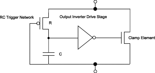
4.3 Design Synthesis of ESD Power Clamp – The ESD Power Clamp Shunting Element
For ESD protection power clamps, two basic functions are the trigger network and the “shunt” network (e.g., also referred to as the “clamp element”) [14, 15]. The role of the shunt element is to provide a current path in the alternative current loop to discharge the ESD current. For the effectiveness of the ESD power clamp, there are a few desired features of the ESD clamp element:
- Low Impedance: Provide a low-impedance path (e.g., a low “on resistance”).
- ESD Robustness: Provide an ESD-robust solution (e.g., discharge the ESD current without failure below the desired ESD specification).
- Scalable: Scalable element with physical size (e.g., width, length, perimeter, or area).
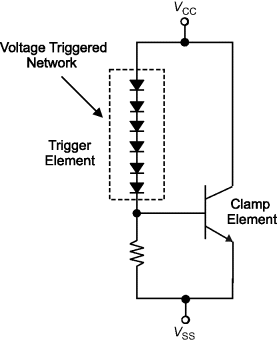
As shown in Figures 4.3 and 4.4, in the ESD protection power clamps, the “shunt” network (e.g., or “clamp element”) is shown. In Figure 4.3, the shunt element is a MOSFET device whereas in Figure 4.4, the shunt element is a bipolar transistor.
Figure 4.3 Example of frequency-triggered ESD power clamp highlighting the trigger network
Figure 4.4 Example of voltage-triggered ESD power clamp highlighting the trigger network
There are some additional desired characteristics of the ESD power clamp “shunt element.” These consist of the following:
- ESD power clamp trigger condition vs. ESD power clamp shunt failure.
- ESD clamp element ESD robustness width scaling.
- ESD on-resistance.
4.3.1 ESD Power Clamp Trigger Condition vs. Shunt Failure
For proper operation of the ESD power clamp, the trigger network will require to initiate prior to the over-voltage or over-current of the ESD “shunt” clamp element [14, 15]. In the frequency domain, if the ESD network trigger does not respond to a specific ESD event, the trigger network will not respond effectively, and the ESD “shunt clamp” will discharge according to its native breakdown event. For a MOSFET “shunt” element, the element will undergo MOSFET drain-to-source snapback. For a bipolar transistor, the bipolar element will undergo collector-to-emitter breakdown.
4.3.2 ESD Clamp Element – Width Scaling
It is desirable to have the ESD results scale with the ESD clamp “shunt” element size. The ESD robustness will scale with the physical width given the following conditions:
- Frequency tuning: Proper frequency “tuning” of the trigger network (e.g., responsive to the ESD event) for MOSFET gate-driven networks or bipolar base-driven networks.
- Drive Circuit: Adequate current drive and current-drive distribution for bipolar base-driven networks.
- Layout Symmetry: Layout optimization of clamp element.
- Ballasting: MOSFET drain ballast (or bipolar emitter ballast) adequate to provide uniformity.
- Power Bus Connectivity: Electrical connection to power bus and ground rail well distributed in the ESD power clamp “clamp element” region of the circuit.
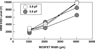
Figure 4.5 shows an example of a MOSFET power clamp width scaling for HBM pulse events [3, 4]. The plot shows the improvement of the HBM ESD robustness with the increase in the power clamp width. In this study, the size of the trigger network and drive circuitry was fixed.
Figure 4.5 Example of ESD MOSFET power clamp width scaling
4.3.3 ESD Clamp Element – On-Resistance
It is desirable to have an ESD clamp on-resistance which reduces with the size of the MOSFET or bipolar clamp element. The lower the ESD clamp on-resistance, the lower the total resistance through the alternative current loop. The lower the resistance in the ESD current loop, the lower the node voltage at the bond pad node. As the impedance of the power bus and the ESD clamp element is reduced, the allowed resistance for the ESD signal pin network can be higher and achieve the same signal pin ESD robustness. Hence, lowering the ESD power clamp resistance allows for a smaller ESD network at the signal pin (e.g., smaller network with lower capacitance).
The ESD clamp on-resistance will scale down with the clamp element device size, given that the element does not undergo current saturation effects, self-heating, or poor current distribution. Hence, if the ESD power clamp element is large enough, and self-heating is kept to a minimum, the “on-resistance” will scale with the width scaling.
4.3.4 ESD Clamp Element – Safe Operating Area
The ESD “clamp element” must remain in the SOA of the device to avoid failure of the ESD power clamp network. To avoid electrical failure of the ESD clamp element prior to achieving the ESD objective, the clamp element of the ESD power clamp must remain below a voltage absolute maximum (VABS MAX) and a current absolute maximum (IABS MAX) of the clamp element.
ESD power clamps have some unique issues as a result of being placed within the power grid of a semiconductor chip. The issues will be discussed briefly, followed by examples in future sections on how to address these issues.
4.4.1 ESD Power Clamp Issues – Power-Up and Power-Down
ESD power clamps are to remain in an “off-state” when a semiconductor chip is in a power-up state, a power-down state, and in a quiescent powered state [14, 15]. The different solutions to avoid initiation of the power clamps during power-up and power-down ramping are as follows:
- Frequency Window: Trigger networks do not respond to these frequencies.
- Feedback Networks: Feedback networks are placed to avoid response to power-up.
- Enable/Disable Functions: Logic can be integrated into the trigger network to “enable” or “disable” the ESD power clamp as desired.
4.4.2 ESD Power Clamp Issues – False Triggering
ESD power clamps can be “false triggered” as a result of pulse events from signals, over-current, over-voltage, or “spikes” during test, burn-in, or other reliability stresses [10, 16, 33–36]. The different solutions to avoid initiation of the power clamps during power-up and power-down are as follows:
- Over-current Protection: Over-current protection can be integrated to avoid the ESD power clamp outside its SOA.
- Frequency Window: Trigger networks do not respond to these frequencies of “spikes.”
- Feedback Networks: Feedback networks are placed with hysteresis.
- Enable/Disable Functions: Logic can be integrated into the trigger network to “enable” or “disable” the ESD power clamp as desired.
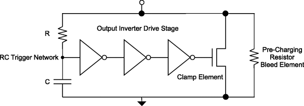
4.4.3 ESD Power Clamp Issues – Pre-Charging
Pre-charging events can occur during ESD testing that can influence the ESD power clamp networks [5–52]. In the process of ESD testing, poor isolation of the test source from the DUT can lead to a pre-charging phenomenon in the semiconductor chip. After an ESD pulse is applied, a low-level current bleeds from the high-voltage source to the DUT without proper “switch” isolation. The “pre-charging” solution is as follows:
- ESD Power Clamp Pre-charge “Bleed” Device: A high-impedance element can be placed in parallel with the ESD power clamp to allow the bleeding of charge from the VDD to the VSS power rail. The “bleed device” can be a resistor. This can be placed locally to the device or non-locally to the ESD power clamp.
- ESD Test System Modification: Modification of the ESD stress test system by providing proper isolation.
4.4.4 ESD Power Clamp Issues – Post-Charging
A post-charging event from ESD simulators is also present that can influence the ESD test results [50–52]. After the ESD event occurs, a low-level current “tail” exists in the simulators that continues to charge the signal pins or power pins. In the process of ESD testing, poor isolation of the test source from the DUT can lead to a post-charging phenomenon in the semiconductor chip. As in the pre-charging event, the post-charging event can lead to an anomalous ESD test result.
In this section, examples of different circuit topologies will be shown to highlight some of the previously discussed issues. Native power supply voltage and non-native ESD power clamps will be discussed.
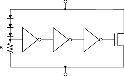
4.5.1 Native Power Supply RC-Triggered MOSFET ESD Power Clamp
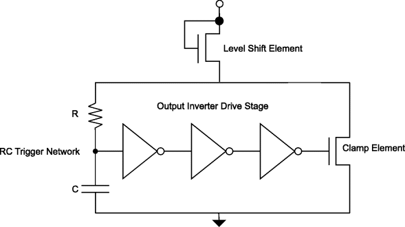
Figure 4.6 shows an example of the most commonly used ESD power clamp in the semiconductor industry, the RC-triggered MOSFET ESD power clamp. The RC-discriminator network discriminates between ESD events and spurious events, or power-up and power-down if properly tuned. The RC trigger is typically “tuned” to respond to the ESD HBM and MM pulse events [2–4, 14, 15].
Figure 4.6 RC-triggered MOSFET ESD power clamp

The inverter stage serves two purposes [14, 15]. First, it allows for the tuning of the RC network without the loading of the first inverter gate capacitance influencing the RC “tuning.” Second, it serves as a drive stage for “driving” the ESD clamp element. In recent years, to improve the responsiveness, the three inverter stages have been reduced to a single stage. The advantage of this is to improve the responsiveness. The disadvantage of the single inverter is the increase in size of the single inverter stage, and the lack of isolation between the RC-discriminator tuning and the load of the inverter stage, and output network. This network is also suitable for native voltage conditions. Given higher voltage power domains, all elements in the circuitry must be voltage-tolerant to that given power domain.
4.5.2 Non-Native Power Supply RC-Triggered MOSFET ESD Power Clamp
Figure 4.7 shows an example of an ESD power clamp for mixed-voltage semiconductor chips [3, 4, 6]. In many mixed-voltage or mixed-signal applications, different power clamps are required based on the voltage of the power domain. Figure 4.7 shows an RC-triggered MOSFET power clamp, where a second MOSFET is used to lower the voltage across all the elements in the lower element. In the design synthesis of this network, the “drop-down” device lowers the voltage across all elements in the ESD power clamp. Hence, it provides two roles: (1) it serves as a “level shift” of the voltage level; (2) it converts the power bus of the ESD network into a “dummy ESD power rail bus” instead of the actual power rail bus. In this case, a MOSFET is used for the “level” shifting network. Alternative ESD “level” shift elements utilized can include diode string elements.
Figure 4.7 Series cascode RC-triggered MOSFET ESD power clamp
4.5.3 ESD Power Clamp Networks with Improved Inverter Stage Feedback
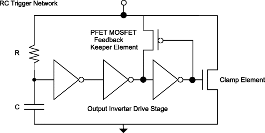
To provide better control of the ESD clamp element, and avoid false triggering, the “latching characteristics” of the inverter drive stage can apply well-known feedback methods. Well-known feedback techniques in CMOS logic include “half-latch” or “full-latch” circuit concepts. Figure 4.8 shows an example of an ESD power clamp with a CMOS half-latch PMOS keeper element. This provides improved control of the MOSFET output gate, which can improve intolerance to false triggering, or avoid low-level leakage of the output MOSFET [9, 10, 34–36].
Figure 4.8 CMOS RC-trigger clamp with CMOS PFET half-latch keeper feedback
A second method to improve the “latching characteristics” of the inverter drive stage can apply well-known “full-latch” circuit concepts. Figure 4.9 shows an example of an ESD power clamp with a CMOS full-latch feedback network [9, 10, 34–36]. The integration of the full inverter for the feedback forms a “SRAM-like” latch between the ESD power clamp last inverter and the feedback inverter. As with the “half-latch” feedback, this provides improved control of the MOSFET output gate, which can improve intolerance to false triggering, or avoid low-level leakage of the output MOSFET.
Figure 4.9 CMOS RC-trigger clamp with CMOS PFET full-latch keeper feedback

Other techniques for improving the control of the ESD power clamp from false triggering can be applied. As the feedback is brought to the earlier stages, the size of the feedback elements can be reduced. A third method is placement of a PMOS device above the inverters. Figure 4.10 shows an example of an ESD power clamp with a PMOS element within the logic [9, 10, 34–36].
Figure 4.10 CMOS RC-trigger clamp with CMOS PFET cascade feedback

4.5.4 ESD Power Clamp Design Synthesis – Forward Bias Triggered ESD Power Clamps
In some applications, the presence of a frequency-triggered network is undesirable – in the integration of an RC-triggered ESD MOSFET network into an RF application [4]. For example, given that the frequency response of the system, such as a cell phone, is pre-defined, it may not be advisable to place another frequency-dependent circuit in a small system (e.g., altering the frequency response of the poles and zeros in the frequency domain). As a result, some circuit design teams desire voltage-triggered networks for RF CMOS instead of frequency-triggered networks. Figure 4.11 is an example of a forward-bias voltage-triggered ESD MOSFET network. The advantage of this network responds to all over-voltage events or over-current conditions. The number of diodes is chosen to turn on prior to the MOSFET snapback voltage of the ESD clamp element. This network has a wide frequency window and is not sensitive to power-up, power-down, or false triggering events, and does provide over-current and over-voltage protection.
Figure 4.11 Forward-bias voltage-triggered ESD power clamps
4.5.5 ESD Power Clamp Design Synthesis – IEC 61000-4-2 Responsive ESD Power Clamps
For applications that are required to respond to the IEC 61000-4-2 pulse event, not all circuit topologies are suitable. For the IEC 61000-4-2 event, there is a fast current pulse which is of considerable magnitude. Hence, to address the frequency response and current magnitude, many ESD power clamps are required to be modified.
During the IEC 61000-4-2 event on the chassis or ground line of a system, a negative pule occurs on the VSS power rail or substrate. This can initiate the RC-triggered network from the negative pulse event. But, the elements in the RC discriminator must be responsive, or circuit failure can occur. The resistor and capacitor element choices must be responsive. Resistors, such as polysilicon resistors, may be slow to respond to fast events.
Figure 4.12 is an example of an IEC 61000-4-2 event-responsive ESD MOSFET network. The advantage of this network is that the p-channel MOSFET is more responsive than a polysilicon resistor element. Additionally, so that the inverter drive network is more responsive, only a single inverter stage is implemented.
Figure 4.12 IEC 61000-4-2 responsive ESD power clamp
4.5.6 ESD Power Clamp Design Synthesis – Pre-Charging and Post-Charging Insensitive ESD Power Clamps
ESD test systems or residual charge can influence the “state” of an RC-triggered MOSFET clamp before or after ESD stress [50–52]. With charge on the VDD power rail, the voltage state of the RC-triggered MOSFET can be pre-charged, and close the MOSFET snapback voltage of the ESD clamp device. On the first discovery of this issue, it was noted by R. Ashton that products with RC-triggered power clamps which were inherently “leaky” had better ESD results than products whose VDD leakage was low. It was from this that Ashton discovered the issue of an ESD test system leading to residual charge on the power grid of the semiconductor chip, influencing the pre-state of the ESD power clamp. It was noted that the charge on the VDD power rail led to the MOSFET snapback of the output device prior to initiation of the RC discriminator response.
Figure 4.13 is an example of an ESD power clamp network with a “bleed” element to provide discharging of the ESD pre-charging event, or a post-charging event. Placing a high-impedance element that bleeds the charge off the power rail can avoid the ESD test system-induced operation failure of the ESD power clamp element.
Figure 4.13 Pre-charging and post-charging insensitive ESD power clamp
4.6 ESD Power Clamp Design Synthesis – Bipolar ESD Power Clamps
Bipolar and bipolar-CMOS (BiCMOS) technologies are used today for analog and mixed-signal semiconductor chips. In a mixed-signal semiconductor chip that utilizes bipolar transistors, analog and digital domains are separated. Bipolar transistors typically have a higher power supply voltage. Additionally, in many bipolar applications, a negative power supply voltage is also used. For these bipolar power domains, bipolar power clamps are used [3, 4, 10, 12–14, 37–44].
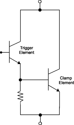
4.6.1 Bipolar ESD Power Clamps with Zener Breakdown Trigger Element
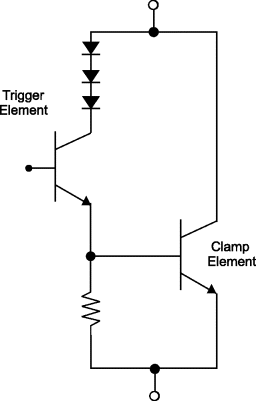
Figure 4.14 is an example of a bipolar ESD power clamp [38, 39]. In this ESD bipolar power clamp, a single transistor is placed between the two power supplies in a collector-to-emitter configuration. The transistor is to be used to discharge the ESD current from the VCC power rail to the VSS ground rail. The trigger element is a Zener diode which undergoes electrical breakdown. When the voltage across the trigger element reaches the breakdown voltage of the Zener diode, the current flows through the Zener diode and into the base of the bipolar transistor. This base-driven network responds to over-voltage conditions in the semiconductor chip. Since it is a voltage-triggered network, it has a wide frequency window of operation; the frequency response is limited to the frequency response of the Zener diode, and its bipolar transistor.
Figure 4.14 Reverse-breakdown Zener-triggered bipolar ESD power clamps

4.6.2 Bipolar ESD Power Clamps with Bipolar Transistor BVCEO Breakdown Trigger Element
Figure 4.15 is an example of a BVCEO voltage-triggered bipolar ESD power clamp. In this ESD bipolar power clamp, a single transistor is placed between the two power supplies in a collector-to-emitter configuration [3, 4, 40–42]. A second transistor is used as the trigger element and is also placed in a common emitter (C-E) configuration. The clamp transistor element is a high-breakdown (HB) transistor, and is to be used to discharge the ESD current from the VCC power rail to the VSS ground rail. The trigger element is a low breakdown (LB) voltage (e.g., BVCEO) npn transistor which undergoes electrical breakdown. When the voltage across the trigger element reaches the BVCEO breakdown voltage, the current flows through the trigger element and into the base of the bipolar transistor. This base-driven network responds to over-voltage conditions in the semiconductor chip. Since it is a voltage-triggered network, it has a wide frequency window of operation; the frequency response is limited to the frequency response of the two transistors.
Figure 4.15 Bipolar ESD power clamps with BVCEO breakdown trigger element
4.6.3 Bipolar ESD Power Clamps with BVCEO Bipolar Transistor Trigger and Variable Trigger Diode String Network
One of the limitations of breakdown-triggered networks is that the breakdown voltage is the native voltage of the element. Hence, it is an advantage to provide a variable trigger voltage for different power supply conditions [3, 4, 41]. Figure 4.16 is an example of a bipolar ESD power clamp with a variable trigger condition. In this ESD bipolar power clamp, a single transistor is placed between the two power supplies in a collector-to-emitter configuration. A series of diode elements (in forward-bias state) and a second transistor is placed in a C-E configuration. The clamp transistor element is a high-breakdown transistor, and is to be used to discharge the ESD current from the VCC power rail to the VSS ground rail. The trigger network is a forward-biased diode string and a low-breakdown voltage (e.g., BVCEO) npn transistor. When the voltage across the trigger network reaches the sum of the forward diode voltage of the diode string and the BVCEO breakdown voltage of the npn transistor, the current flows through the trigger element and into the base of the bipolar transistor. This base-driven network responds to over-voltage conditions in the semiconductor chip. Since it is a voltage-triggered network, it has a wide frequency window of operation; the frequency response is limited to the frequency response of the two transistors.
Figure 4.16 Bipolar ESD power clamp with BVCEO breakdown trigger element and diode string elements
4.6.4 Bipolar ESD Power Clamps with Frequency Trigger Elements
One of the limitations of breakdown-triggered networks is that the power supply voltage must reach the breakdown voltage prior to initiating the ESD power clamp. Frequency-triggered networks can be established using bipolar devices. Figure 4.17 is an example of a bipolar ESD power clamp with a capacitively coupled trigger network [43, 44].
Figure 4.17 Capacitive-triggered bipolar ESD power clamp
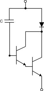
In this ESD bipolar power clamp, two transistors are placed in a Darlington configuration, with a capacitor element as part of the trigger network. The capacitor is placed between the power supply and the capacitor of the first transistor stage in the Darlington network. A second transistor is placed in a Darlington C-E configuration. A diode, used to drop voltage across the single transistor, is placed between the two power supplies in a collector-to-emitter configuration. This base-driven network responds to frequency conditions in the semiconductor chip. Since it is a frequency-triggered network, it has a smaller ESD power clamp frequency window of operation; the frequency response is defined by the capacitor element.
4.7 Master/Slave ESD Power Clamp Systems
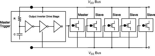
ESD power clamps can be lumped or distributed through a semiconductor chip. In the case of a distributed system, a design synthesis concept is to provide a single trigger element for many ESD “clamp” elements [10]. There are two advantages of this concept. First, a single trigger will initiate all elements in parallel, instead of independent triggers which may vary across a semiconductor chip. Second, there is a saving of semiconductor chip area. Figure 4.18 shows a high-level diagram of the master/slave ESD system for a full-chip ESD design implementation. In this implementation, only one trigger element exists.
Figure 4.18 ESD power clamp master/slave system

Figure 4.19 shows a master/slave ESD system for a full-chip ESD design implementation using an RC-triggered MOSFET network. In this implementation, only one RC-trigger element and one drive circuit is used. In this fashion, all MOSFET gate connections can be triggered simultaneously, and the trigger network area is saved around the semiconductor chip. For this network system to be effective, the electrical connectivity between the MOSFET gate drive network and all the ESD clamp elements must be provided with low resistance bussing around the semiconductor chip.
Figure 4.19 ESD power clamp master/slave system
4.8 Summary and Closing Comments
In this chapter, the discussion focuses on ESD power clamp networks. A key issue in ESD design synthesis is the type of ESD network used in the power grid domain. This was discussed briefly in previous chapters, and this entire chapter is dedicated to ESD power clamp discussions, circuit topology, and issues. There is a vast amount of publications and literature in this area.
In Chapter 5, the discussion focuses on ESD networks on the signal pads. In this case, the entire chapter will be dedicated to ESD signal pin device layout and design.
Problems
4.1. What are the advantages and disadvantages of reverse-bias triggered ESD power clamps? Are they scalable? How does one make a reverse-bias triggered ESD network scalable with power supply and technology scaling?
4.2. What are the advantages and disadvantages of forward-bias triggered ESD power clamps? Are they scalable? How does one make a reverse-bias triggered ESD network scalable?
4.3. A bipolar transistor open-base collector-to-emitter breakdown voltage (BVCEO) is inversely proportional to the unity current gain cutoff frequency (according to the well-known Johnson limit relationship). How can this be synthesized and utilized for ESD protection in ESD power clamps? Show an example of this. Show how this can be used in technology scaling for bipolar technology.
4.4. Show an example of an RC-triggered ESD power clamp containing three inverter stages: resistor, capacitor, and NFET output clamp. What are the concerns? Discuss false-triggering concerns, power-up, power-down, latchup, and electrical overstress issues. What elements in this network can form a parasitic pnpn and form a latchup issue? How does this network respond to increased temperature?
4.5. Show an example of an RC-triggered ESD power clamp containing three inverter stages: resistor, capacitor, and PFET output clamp. What are the concerns? Discuss false-triggering concerns, power-up, power-down, latchup, and electrical overstress issues. What elements in this network can form a parasitic pnpn and form a latchup issue? How does this network respond to increased temperature?
4.6. In a mixed-voltage application, with two MOSFET transistors there are two choices in the construction of RC-triggered clamps: (a) use of only the higher-voltage MOSFET; or (b) cascode of the low-voltage output. What are the tradeoffs, performance, over-voltage, and area considerations between the two implementations?
4.7. In a bipolar power application, the signal is required to swing from a positive to a negative voltage (e.g., from VCC to VEE, where VCC = +5 V and VEE =− 5 V). Show multiple configurations for ESD networks in a three-rail architecture with VCC, VSS, and VEE power rails.
4.8. A 5.0 V ESD MOSFET RC-triggered power clamp is re-mapped from a 3.3 V MOSFET power clamp. What adjustments are made in the re-mapping from an over-voltage case? In the MOSFET output transistor size, on-resistance, channel length, and area? Show the terms in the MOSFET current model that are influenced.
4.9. In the operation of the circuit, show the resistances in the alternative current path assuming a turn-on voltage and on-resistance for the ESD input network, power bus, and ESD power clamp. Discuss the area and placement tradeoffs between the power bus, input device, and ESD power clamp elements. What are the competing factors?
4.10. As technologies scale, the ESD input device is required to scale to smaller dimensions. Assuming the on-resistance of the ESD device increases as R ′ = Rα (where α is the constant electric field scaling theory), how should the ESD power bus resistance and ESD power clamp resistance scale accordingly to maintain a constant ESD protection level (e.g., constant ESD scaling theory)?
4.11. As technologies scale, assume the voltage scaling on the input node is as V ′ = V/α, where VBR′ = VBR/α (where α is the constant electric field scaling theory); also, the ESD input device is required to scale to smaller dimensions. Assume the on-resistance of the ESD device increases as R ′ = R/α. How should the ESD power bus resistance and ESD power clamp resistance scale accordingly to maintain a constant ESD protection level (e.g., constant ESD scaling theory)? Given the bus width is also scaled, as W ′ = W/α, show that the placement requirement is modified to maintain constant ESD results. (Hint: derive the placement relationship of the ESD input device to power clamp based on α scaling theory.)
1. A. Amerasekera and C. Duvvury. ESD in Silicon Integrated Circuits. Chichester, UK: John Wiley and Sons, Ltd, 1995.
2. S. Voldman. ESD: Physics and Devices. Chichester, UK: John Wiley and Sons, Ltd, 2004.
3. S. Voldman. ESD: Circuits and Devices. Chichester, UK: John Wiley and Sons, Ltd, 2005.
4. S. Voldman. ESD: RF Technology, and Circuits. Chichester, UK: John Wiley and Sons, Ltd, 2006.
5. S. Voldman. ESD: Failure Mechanisms and Models. Chichester, UK: John Wiley and Sons, Ltd, 2009.
6. S. Dabral and T. J. Maloney. Basic ESD and I/O Design. New York: John Wiley and Sons, Inc., 1998.
7. R. Troutman. Latchup in CMOS Technology: The Problem and the Cure. New York: Kluwer Publications, 1986.
8. S. Voldman. Latchup. Chichester, UK: John Wiley and Sons, Ltd, 2009.
9. M. D. Ker and S. F. Hsu. Transient-Induced Latchup in CMOS Integrated Circuits. Singapore: John Wiley and Sons (Asia) Pte Ltd, 2009.
10. V. Vashchenko and A. Shibkov. ESD Design for Analog Circuits. New York: Springer, 2010.
11. N. Maene, J. Vandenbroeck, and L. Van dem Bempt. On chip electrostatic discharge protections for inputs, outputs, and supplies of CMOS circuits. Proceedings of the Electrical Overstress/Electrostatic Discharge (EOS/ESD) Symposium, 1992; 228– 233.
12. G. D. Croft. Dual rail ESD protection using complementary SCRs. Proceedings of the Electrical Overstress/Electrostatic Discharge (EOS/ESD) Symposium, 1992; 243– 249.
13. G. D. Croft. ESD protection using SCR clamping. U.S. Patent No. 5,574,618, November 12, 1996.
14. W. Mack and R. Meyer. New ESD protection schemes for BiCMOS processes with application to cellular radio designs. Proceedings of the IEEE International Symposium on Circuits and Systems, 1992.
15. R. Merrill and E. Issaq. ESD design methodology. Proceedings of the Electrical Overstress/Electrostatic Discharge (EOS/ESD) Symposium, 1993; 233– 238.
16. S. Dabral, R. Aslett, and T. Maloney. Designing on-chip power supply coupling diodes for ESD protection and noise immunity. Proceedings of the Electrical Overstress/Electrostatic Discharge (EOS/ESD) Symposium, 1994; 239– 249.
17. G. D. Croft. ESD protection using a variable voltage supply clamp. Proceedings of the Electrical Overstress/Electrostatic Discharge (EOS/ESD) Symposium, 1994; 135– 140.
18. D. Krakauer, K. Mistry, and H. Partovi. Circuit interaction during electrostatic discharge. Proceedings of the Electrical Overstress/Electrostatic Discharge (EOS/ESD) Symposium, 1994; 113– 119.
19. N. Tanden. ESD trigger circuit. Proceedings of the Electrical Overstress/Electrostatic Discharge (EOS/ESD) Symposium, 1994; 120– 124.
20. S. Dabral, R. Aslett, and T. Maloney. Core clamps for low voltage technologies. Proceedings of the Electrical Overstress/Electrostatic Discharge (EOS/ESD) Symposium, 1994; 141– 149.
21. S. Voldman. ESD protection in a mixed voltage interface and multi-rail disconnected power grid environment in 0.5- and 0.25-µm channel length CMOS technologies. Proceedings of the Electrical Overstress/Electrostatic Discharge (EOS/ESD) Symposium, 1994; 125– 134.
22. T. Maloney. Novel clamp circuits for IC power supply protection. Proceedings of the Electrical Overstress/Electrostatic Discharge (EOS/ESD) Symposium, 1995; 1– 12.
23. E. Worley, R. Gupta, B. Jones, R. Kjar, C. Nguyen, and M. Tennyson. Sub-micron chip ESD protection schemes which avoid avalanche junctions. Proceedings of the Electrical Overstress/Electrostatic Discharge (EOS/ESD) Symposium, 1995; 13– 20.
24. G. D. Croft. Transient supply clamp with a variable RC time constant. Proceedings of the Electrical Overstress/Electrostatic Discharge (EOS/ESD) Symposium, 1996; 276– 279.
25. J. Smith. A substrate triggered lateral bipolar circuit for high voltage tolerant ESD protection applications. Proceedings of the Electrical Overstress/Electrostatic Discharge (EOS/ESD) Symposium, 1998; 63– 71.
26. W. Anderson, J. Monanaro, and N. Howorth. Cross-referenced ESD protection supplies. Proceedings of the Electrical Overstress/Electrostatic Discharge (EOS/ESD) Symposium, 1998; 86– 96.
27. M. D. Ker. Whole chip ESD protection design with efficient VDD-to-VSS clamp circuit for submicron CMOS VLSI. IEEE Transactions on Electron Devices. ED-46 (1), 1999; 173–183.
28. T. Maloney. Stacked PMOS clamps for high voltage power supply protection. Proceedings of the Electrical Overstress/Electrostatic Discharge (EOS/ESD) Symposium, 1999; 70– 77.
29. S. Poon and T. Maloney. New considerations for MOSFET power clamps. Proceedings of the Electrical Overstress/Electrostatic Discharge (EOS/ESD) Symposium, 2002; 1– 5.
30. T. Maloney, S. Poon, and L. Clark. Methods for designing low-leakage power supply clamps. Proceedings of the Electrical Overstress/Electrostatic Discharge (EOS/ESD) Symposium, 2003; 27– 43.
31. J. Smith and G. Boselli. A MOSFET power clamp with feedback enhanced triggering for ESD protection in advanced CMOS technologies. Proceedings of the Electrical Overstress/Electrostatic Discharge (EOS/ESD) Symposium, 2003; 8– 16.
32. M. Stockinger, J. Miller, M. Khazhinsky, C. Torres, J. Weldon, B. Preble, M. Bayer, M. Akers, and V. Kamat. Boosted and distributed rail clamp networks for ESD protection in advanced CMOS technologies. Proceedings of the Electrical Overstress/Electrostatic Discharge (EOS/ESD) Symposium, 2003; 17– 26.
33. M. Stockinger and J. Miller. Advanced ESD rail clamp network design for high voltage CMOS applications. Proceedings of the Electrical Overstress/Electrostatic Discharge (EOS/ESD) Symposium, 2003; 280– 288.
34. P. Tong, W. Chen, and R. Jiang. Active ESD shunt with transistor feedback to reduce latchup susceptibility or false triggering. Proceedings of the IEEE International Symposium on the Physical and Failure Analysis of Integrated Circuits (IPFA), 2004; 89– 92.
35. M. D. Ker and S. F. Hsu. Component-level measurement for transient-induced latchup in CMOS ICs under system-level ESD considerations. IEEE Transactions on Device and Materials Reliability, 6 (3), 2006; 461–472.
36. C. C. Yen and M. D. Ker. Failure of on-chip power-rail ESD clamp circuits during system-level ESD test. Proceedings of the International Reliability Physics Symposium (IRPS), 2007; 598– 599.
37. J. Z. Chen, X. Y. Zhang, A. Amerasekera, and T. Vrotsos. Design and layout of a high ESD performance NPN structure for submicron BiCMOS/bipolar circuits. Proceedings of the International Reliability Physics Symposium (IRPS), 1996; 227– 232.
38. S. Joshi, P. Juliano, E. Rosenbaum, G. Katz, and S. M. Kang. ESD protection for BiCMOS circuits. Proceedings of the Bipolar Circuit Technology Meeting (BCTM), 2000; 218– 221.
39. S. Joshi, R. Ida, P. Givelin, and E. Rosenbaum. An analysis of bipolar breakdown and its application to the design of ESD protection circuits. Proceedings of the International Reliability Physics Symposium (IRPS), 2001; 240– 245.
40. S. Voldman, A. Botula, and D. Hui. Silicon germanium heterojunction bipolar transistor ESD power clamps and the Johnson limit. Proceedings of the Electrical Overstress/Electrostatic Discharge (EOS/ESD) Symposium, 2001; 326– 336.
41. S. Voldman. Variable trigger voltage ESD power clamps for mixed voltage applications using a 120 GHz/100 GHz (fT/fMAX) silicon germanium heterojunction bipolar transistor with carbon incorporation. Proceedings of the Electrical Overstress/Electrostatic Discharge (EOS/ESD) Symposium, 2002; 52– 61.
42. S. Voldman and E. Gebreselasie. Low-voltage diode-configured SiGe:C HBT triggered ESD power clamps using a raised extrinsic base 200/285 GHz (fT/fMAX) SiGe:C HBT device. Proceedings of the Electrical Overstress/Electrostatic Discharge (EOS/ESD) Symposium, 2004; 57– 66.
43. Y. Ma and G. P. Li. A novel on-chip ESD protection circuit for GaAs HBT RF power amplifiers. Proceedings of the Electrical Overstress/Electrostatic Discharge (EOS/ESD) Symposium, 2002; 83– 91;
and Journal of Electrostatics, 59, October 2003; 211–227.
44. Y. Ma G. P. Li. InGaP/GaAs HBT DC-20 GHz distributed amplifier with compact ESD protection circuits. Proceedings of the Electrical Overstress/Electrostatic Discharge (EOS/ESD) Symposium, 2004; 50– 54.
45. C. Duvvury. F. Carvajal, C. Jones, and M. Smayling. Device integration for ESD robustness of high voltage power MOSFETs. International Electron Device Meeting (IEDM) Technical Digest, 1994; 407–410.
46. M. Mergens, W. Wilkening, S. Mettler, et al. Analysis of lateral DMOS power devices under ESD stress conditions. IEEE Transactions on Electron Devices, ED-47, 2000; 2128–2137.
47. V. De Heyn, G. Groeseneken, B. Keppens, et al. Design and analysis of new protection structures for smart power technology with controlled trigger and holding voltage. Proceedings of the International Reliability Physics Symposium (IRPS), 2001; 253– 258.
48. G. Bertrand, C. Delage, M. Bafluer, et al. Analysis and compact modeling of a vertical grounded base npn transistor used as ESD protection in a smart power technology. IEEE Journal of Solid State Circuits, 36, 2001; 1373–1381.
49. J. H. Lee, J. R. Shih, C. S. Tang, et al. Novel ESD protection structure with embedded SCR LDMOS for smart power technology. Proceedings of the International Reliability Physics Symposium (IRPS), 2002; 156– 161.
50. C. Duvvury, R. Steinhoff, G. Boselli, V. Reddy, H. Kunz, S. Marum, and R. Cline. Gate oxide failures due to anomalous stress from HBM ESD testers. Proceedings of the Electrical Overstress/Electrostatic Discharge (EOS/ESD) Symposium, 2004; 132– 140.
51. T. Meuse, R. Barrett, D. Bennett, M. Hopkins, J. Leiserson, and L. Ting. Formation and suppression of a newly discovered secondary EOS event in HBM test systems. Proceedings of the Electrical Overstress/Electrostatic Discharge (EOS/ESD) Symposium, 2004; 141– 145.
52. R. A. Ashton, B. E. Weir, G. Weiss, and T. Meuse. Voltages before and after HBM stress and their effect on dynamically triggered power supply clamps. Proceedings of the Electrical Overstress/Electrostatic Discharge (EOS/ESD) Symposium, 2004; 153– 159.