
First-order CR and LR circuits
Introduction
There are two first-order CR and two first-order LR circuits which we will consider here. One circuit of each type forms an integrator, or a low-pass filter, and one a differentiator, or a high-pass filter. All four circuits can be considered to be variations on the voltage dividers which we looked at in Chapter 8. In each case, either the input resistor or the output resistor is replaced with either a capacitor or an inductor.
Where we call them integrators and differentiators we will look at their output waveforms when their input is a pulse. This is called the time response. Then we will consider their action as filters; that is, we will look at the amplitude and phase of their outputs when the input is a sine wave of varying frequency. This is the frequency response.
The two approaches are in fact different ways of looking at the same thing, which is their transfer function – in other words their output for any given input. Both methods can be both understood and quantified without much mathematics, and one, other or both is usually very helpful when we need to use them in a circuit, or understand their use.
Time response
A quick explanation of CR and LR circuit waveforms
The four circuits, with their associated waveforms, are shown in Figure 9.1.

We assume that the resistance of the source is negligible, and the load on the circuit is high enough to be ignored. Both CR circuits have the same current waveform, and so do both LR circuits. (As discussed in Chapter 5, the current in a series circuit is the same through each of its components, and putting them in a different order makes no difference to that current.) Also, the sum of the capacitor’s and the resistor’s, or the inductor’s and the resistor’s, voltages always equals the input voltage (by Kirchhoff’s voltage law).
A capacitor will always resist a sudden change in the voltage across its terminals. Hence, when the leading edge of the pulse arrives, its voltage remains, initially, at zero. All of the available voltage is, at that moment, across the resistor. Therefore the current at that moment is ![]() .
.
The current charges the capacitor, causing its voltage to increase from zero. As this happens the voltage across the resistor decreases. The current (proportional always to the voltage across the resistor) falls accordingly. This in turn slows down the charge rate of the capacitor. Hence the rate of change of the voltage across the capacitor decreases as that voltage approaches the input voltage. The current in the circuit falls from ![]() towards zero, and the voltage across the resistor falls from V towards zero.
towards zero, and the voltage across the resistor falls from V towards zero.
Eventually, the capacitor is fully charged, and the voltage across it is equal to the input voltage. Things will stay like this until the input changes again. When it falls to zero the voltage across the cap cannot change instantly; it must now discharge, back through the resistor, and into the source (the only possible path –remember that the source has a low, and the load a high, resistance). Hence a current of ![]() now flows for an instant (the minus sign indicating that the direction has reversed). This current decreases towards zero again as the voltage which created it, that across the plates of the capacitor, falls. Eventually, there is no charge left in the capacitor, no voltage across its terminals and no current in the circuit. The circuit is once again at rest, as it was in the beginning.
now flows for an instant (the minus sign indicating that the direction has reversed). This current decreases towards zero again as the voltage which created it, that across the plates of the capacitor, falls. Eventually, there is no charge left in the capacitor, no voltage across its terminals and no current in the circuit. The circuit is once again at rest, as it was in the beginning.
Because an inductor resists a sudden change in current, an LR circuit’s current is at zero when the leading edge of the pulse arrives. So then is the voltage across the resistor at that moment. For the sum of the resistor’s and the inductor’s voltage to equal the input voltage, as it must, the inductor sets up a back EMF across its terminals, opposing the input voltage. The back EMF decays with time, and current begins to flow in the circuit, creating a voltage across the resistor. Eventually there is no back EMF, and the current arrives at a final value of ![]() The voltage across the inductor is now zero, and the voltage across the resistor is V.
The voltage across the inductor is now zero, and the voltage across the resistor is V.
When the trailing edge of the pulse arrives at the input (i.e. the input voltage falls towards zero again) the current in the circuit also will try to fall to zero. Again the inductor will resist change. To do this it will set up another back EMF, opposing the voltage across the resistor now. This back EMF will also decay with time, allowing the current in the circuit and the voltage across the resistor to fall towards zero.
The only difference between the two CR (or the two LR) circuits is which device, resistor or capacitor (inductor), is on the output side. The voltages across the components, and the currents through them, are identical.
Time constants It can be seen that, essentially, only two waveform shapes exist for both output voltage and for current in all four circuits. These two waveforms are shown in more detail in Figure 9.2.

Figure 9.2 Detail of Figure 9.1
All of the curves are exponential in shape. How long they take to change from initial to final values is determined by the circuit time constant T (not to be confused with the T used for period of an AC waveform), which is in turn a function of component values in the circuit.
The formulae for T are:for a CR circuit:
and for an LR circuit:
T is tabulated for various values of C and R in Table 9.1, and for L and R in Table 9.2. These tables also give values of frequency constants which we will look at later under ‘Frequency response’.

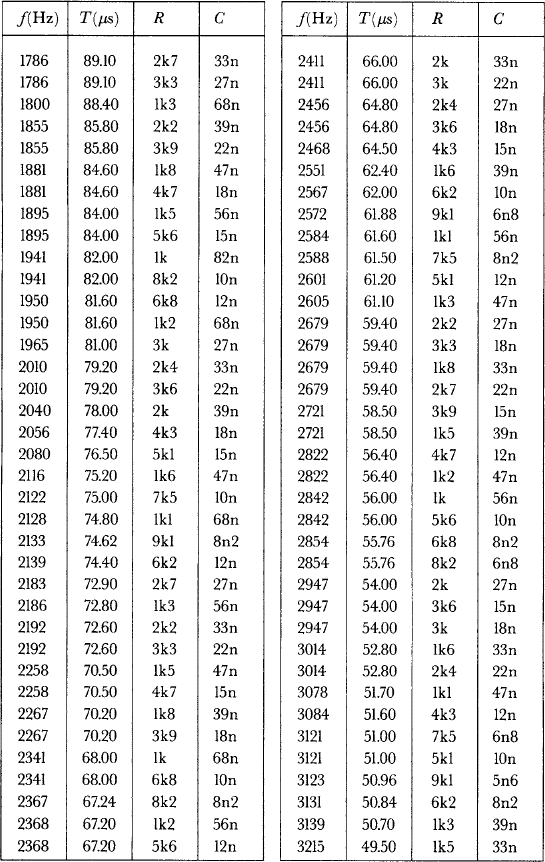


The tables are sorted in order of T, increasing for CR and decreasing for LR. T is given in μs. Should we want to obtain a value of T which is outside the range of the table we should do it by scaling one or both components by factors of 10 appropriately. As always, some examples:
Example 9.1: Find values for a CR circuit with T – 56 ns.
From Table 9.1:

We want T = 56 ns, so we need to make R and C between them 1000 times smaller. We could for example make R = 100 Ω and C = 560p, or R = 56 Ω and C = 1n.
Example 9.2: Find values for an LR circuit with T = 4 μs.
From Table 9.2:
![]()
To make T 10 times smaller we could either make R 10 times larger or L 10 times smaller. So R = 12k and L = 47m or R = 1k2 and L = 4.7m would both work.
Values of voltage and current as a function of t and T Once we have determined a value of T, we can find the value of Vt or It, that is output voltage for any moment in time, t, after the rising or falling edge of the input waveform. The formulae are as follows.
For a curve going from zero to a final value:
and for a curve going back down to zero:
Table 9.3 gives values of Eqns (9.3) and (9.4) for various values of ![]()
Table 9.3
Step response of first-order CR and LR circuits
| 0.1 | 0.9048 | 0.0952 |
| 0.2 | 0.8187 | 0.1813 |
| 0.3 | 0.7408 | 0.2592 |
| 0.4 | 0.6703 | 0.3297 |
| 0.5 | 0.6065 | 0.3935 |
| 0.6 | 0.5488 | 0.4512 |
| 0.7 | 0.4966 | 0.5034 |
| 0.8 | 0.4493 | 0.5507 |
| 0.9 | 0.4066 | 0.5934 |
| 1.0 | 0.3679 | 0.6321 |
| 1.1 | 0.3329 | 0.6671 |
| 1.2 | 0.3012 | 0.6988 |
| 1.3 | 0.2725 | 0.7275 |
| 1.4 | 0.2466 | 0.7534 |
| 1.5 | 0.2231 | 0.7769 |
| 1.6 | 0.2019 | 0.7981 |
| 1.7 | 0.1827 | 0.8173 |
| 1.8 | 0.1653 | 0.8347 |
| 1.9 | 0.1496 | 0.8504 |
| 2.0 | 0.1353 | 0.8647 |
| 2.1 | 0.1225 | 0.8775 |
| 2.2 | 0.1108 | 0.8892 |
| 2.3 | 0.1003 | 0.8997 |
| 2.4 | 0.0907 | 0.9093 |
| 2.5 | 0.0821 | 0.9179 |
| 2.6 | 0.0743 | 0.9257 |
| 2.7 | 0.0672 | 0.9328 |
| 2.8 | 0.0608 | 0.9392 |
| 2.9 | 0.0550 | 0.9450 |
| 3.0 | 0.0498 | 0.9502 |
| 3.1 | 0.0450 | 0.9550 |
| 3.2 | 0.0408 | 0.9592 |
| 3.3 | 0.0369 | 0.9631 |
| 3.4 | 0.0334 | 0.9666 |
| 3.5 | 0.0302 | 0.9698 |
| 3.6 | 0.0273 | 0.9727 |
| 3.7 | 0.0247 | 0.9753 |
| 3.8 | 0.0224 | 0.9776 |
| 3.9 | 0.0202 | 0.9798 |
| 4.0 | 0.0183 | 0.9817 |
| 4.1 | 0.0166 | 0.9834 |
| 4.2 | 0.0150 | 0.9850 |
| 4.3 | 0.0136 | 0.9864 |
| 4.4 | 0.0123 | 0.9877 |
| 4.5 | 0.0111 | 0.9889 |
| 4.6 | 0.0101 | 0.9899 |
| 4.7 | 0.0091 | 0.9909 |
| 4.8 | 0.0082 | 0.9918 |
| 4.9 | 0.0074 | 0.9926 |
| 5.0 | 0.0067 | 0.9933 |
Example 9.3: Find out to what the voltage out from a 2k2, 1μF differentiator will be after 6 ms, when the input is a rising edge of 6 V:
First we calculate T, from Eqn(9.1).
Now we evaluate ![]() . If
. If ![]() . Referring to Figures 9.1 and 9.2, we see that the waveform is a rising edge, governed by the
. Referring to Figures 9.1 and 9.2, we see that the waveform is a rising edge, governed by the ![]() function. So we use Table 9.1 to find a value for that function where
function. So we use Table 9.1 to find a value for that function where ![]() . We find:
. We find:
which is the nearest to 0.27. The final value of the voltage will be 6 V. So its value after 6 ms will be 0.741 × 6 = 4.45 V.
Example 9.4: Design a circuit whose output voltage will be −7 V 220 ms after the falling edge of a + 10 V pulse input. Give a CR and an LR alternative.
By referring to Figure 9.1, we see that the circuit must be a differentiator, as that circuit has an output voltage which goes from – V to 0 after the falling edge of the input. The equation for that curve is ![]() where V = 10 V in this case. So we can write:
where V = 10 V in this case. So we can write:
and we can use Table 9.1 in reverse to find:
Now we know that t = 220 ms, and that ![]() , so we know that
, so we know that ![]() . Now we can use Table 9.3 to find suitable C and R values, and Table 9.4 to find L and R
. Now we can use Table 9.3 to find suitable C and R values, and Table 9.4 to find L and R
From Table 9.3:
![]()
T is in μs, so we need to scale up by ![]() . We could do this by multiplying both C and R by 100. So we get R = 470 k, C = 390 n.
. We could do this by multiplying both C and R by 100. So we get R = 470 k, C = 390 n.
From Table 9.4:
![]()
Here we need to scale by making R smaller and L larger. We could say theoretical values of R = 18 Ω and L = 3.3 H. A 3.3 H inductor would be huge (though not unknown!), which illustrates why CR circuits tend to be more common than LR ones.
Frequency response
Now we look at the behaviour of the same circuits when their input is a continuous sine wave. We are interested in what happens as the frequency of the input is varied.
How first-order filters work
As we saw in Chapter 4, capacitive reactance falls with increasing frequency:
Inductive reactance increases with frequency:
Each obeys Ohm’s Law, in that VC = IXC, or XL = IXL – that is the voltage across a capacitor or an inductor is the current through it multiplied by its reactance, like a resistor. However, whereas voltage and current are in phase with a resistor, they are 90° out of phase with inductors and capacitors.
The four basic filter circuits are shown in Figure 9.3. We can view them all as being similar to the voltage divider which we looked at in Chapter 6, except that one component in each has a ‘resistance’ which varies with frequency. Hence the overall attenuation of each varies with frequency too.
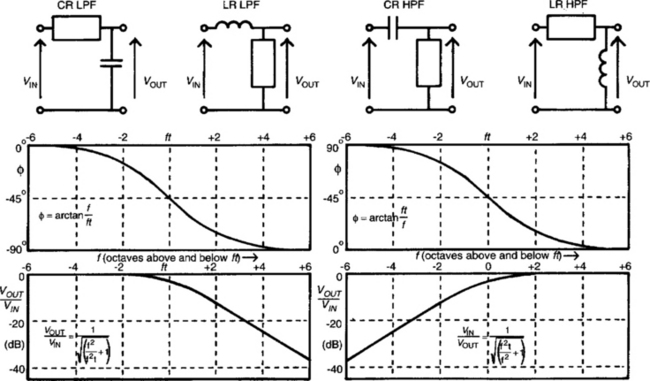
Where the component on the input side of the circuit has higher impedance at higher frequencies, the circuit is a low-pass filter. These are the two circuits on the left hand side of Figure 9.3, a CR with the capacitor across the output or an LR with the inductor on the input. Conversely, a high-pass filter is formed by a CR with the capacitor on the input side or by an LR with the inductor across the output.
Frequency constants The frequency at which the reactance of the capacitor or inductor is the equal to the resistor is known as the ‘turnover frequency’ (ft). The attenuation at this frequency is not 6 dB, as it would be if both components were resistive. Because of the fact that the voltage across the reactive component is 90° out of phase with the voltage across the resistor the attenuation is only 3 dB. The turnover frequency can be calculated from the component values (or component values selected to give a desired ft). The governing formulae are:
or
Values for ft are given in Table 9.1 for CR circuits and in Table 9.2 for LR circuits. As before, component values can be scaled to get frequencies which are outside the range of the table.
Example 9.5: Give component values for a CR filter with ft = 12 kHz.
From Table 9.1:
![]()
We need to multiply the frequency by 10, so we could divide either C or R by 10 to achieve this. So both R = 110 Ω, C = 120n and R = 1k1, C = 12n would do it.
Example 9.6: Give component values for an LR filter with ft = 500kHz. From Table 9.2:
![]()
We need ft 100 times larger, so we can make L smaller and/or R larger. We could choose, for instance, R = 15k, L = 4.7m.
Determining the level and phase at any frequency The level of the output voltage, relative to the input, is determined by the ratio of the signal frequency and ft:
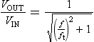
We can see that when f is much less than ft, the value of ![]() is very close to 1, and hence the signal is not much attenuated by the circuit. When
is very close to 1, and hence the signal is not much attenuated by the circuit. When ![]() is much greater than 1, the value of
is much greater than 1, the value of ![]() approximates to:
approximates to:
From this simplified expression, it can be seen that a doubling in frequency will lead to a halving in output signal, or multiplying the input frequency by 10 will reduce its output level to one-tenth. Hence it is customary to say that the filter slope, above the turnover frequency, is −6 db/octave, or−20 dB/decade.
The equation for the attenuation of a HPF is:

and a similar argument applies; this time the slope is −6 dB/octave or−20 dB/decade below the turnover frequency.
These filters affect the relative phase (φ), as well as the level, of the signal. The LPF causes the output signal to be between 0 and 90° lagging the input signal, the HPF 0° to 90° leading. In both cases the phase angle is 45° at ft. These functions are again determined by the ratio of f and ft:
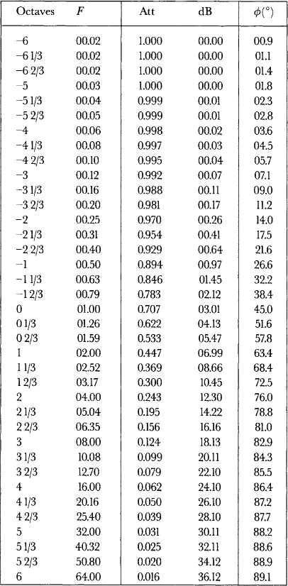
Hence it is possible to predict both attenuation and phase shift through a filter for any given frequency, provided that ft is known. Table 9.4 gives both at intervals of a third of an octave, for six octaves either side of ft.
The first column of Table 9.4 gives the frequency in terms of the number of octaves away from ft. (The minus sign means higher in frequency for an HPF, lower for an LPF.) The second gives the ratio of frequencies, which we call F (ft/f for an HPF, f/ft for an LPF). The third column is the attenuation as the ratio VOUT/VIN, the fourth is attenuation in dBs. The fifth column is the phase shift in degrees.
Example 9.6: What is the approximate attenuation and phase shift at a frequency of 5 kHz for a LPF consisting of a 3n3 capacitor and a 15k resistor?
From Table 9.4:
![]()
Nearest value in the table is 1.59 (2/3 octave) where attenuation is 5.5 dB, phase shift is 58°
Example 9.7: A circuit is needed to low-pass filter a signal such that the level at 100 kHz is 15 dB down on the signal below ft. What would ft be (using the table to get the nearest approximation)? What will the attenuation be at 50 kHz?
From Table 9.4:
![]()
This tells us that for a 14 dB attenuation at 100 kHz, ![]() , so
, so ![]() , or 20 kHz. At 50 kHz
, or 20 kHz. At 50 kHz ![]() or 2.5, and we get:
or 2.5, and we get:
![]()
and the attenuation is 5.5 dB.