
Rick Gentile
With the multimedia revolution in full swing, we’re becoming accustomed to toting around cell phones, PDAs, cameras, and MP3 players, concentrating our daily interactions into the palms of our hands. But given the usefulness of each gadget, it’s surprising how often we upgrade to “the latest and greatest” device. This is, in part, due to the fact that the cell phone we bought last year can’t support the new video clip playback feature touted in this year’s TV ads.
After all, who isn’t frustrated after discovering that his portable audio player gets tangled up over the latest music format? In addition, which overworked couple has the time, much less the inclination, to figure out how to get the family vacation travelogue off their mini-DV camcorder and onto a DVD or hard disk?
As Figure 7.1 implies, we’ve now reached the point where a single gadget can serve as a phone, a personal organizer, a camera, an audio player, and a web-enabled portal to the rest of the world.

But still, we’re not happy.
Let’s add a little perspective: we used to be satisfied just to snap a digital picture and see it on our computer screen. Just 10 years ago, there were few built-in digital camera features, the photo resolution was comparatively low, and only still pictures were an option. Not that we were complaining, since previously our only digital choice involved scanning 35-mm prints into the computer.
In contrast, today we expect multimegapixel photos, snapped several times per second, which are automatically white-balanced and color-corrected. What’s more, we demand seamless transfer between our camera and other media nodes, a feature made practical only because the camera can compress the images before moving them.
Clearly, consumer appetites demand steady improvement in the “media experience.” That is, people want high-quality video and audio streams in small form factors, with low power requirements (for improved battery life) and at low cost. This desire leads to constant development of better compression algorithms that reduce storage requirements while increasing audio/video resolution and frame rates.
To a large extent, the Internet drives this evolution. After all, it made audio, images, and streaming video pervasive, forcing transport algorithms to become increasingly clever at handling ever-richer media across the limited bandwidth available on a network. As a result, people today want their portable devices to be net-connected, high-speed conduits for a never-ending information stream and media show. Unfortunately, networking infrastructure is upgraded at a much slower rate than bandwidth demands grow, and this underscores the importance of excellent compression ratios for media-rich streams.
It may not be readily apparent, but behind the scenes, processors have had to evolve dramatically to meet these new and demanding requirements. They now need to run at very high clock rates (to process video in real time), be very power efficient (to prolong battery life), and comprise very small, inexpensive single-chip solutions (to save board real estate and keep end products price-competitive). What’s more, they need to be software-reprogrammable, in order to adapt to the rapidly changing multimedia standards environment.
Consider the components of a typical media processing system, shown in Figure 7.2. Here, an input source presents a data stream to a processor’s input interface, where it is manipulated appropriately and sent to a memory subsystem. The processor core(s) then interact with the memory subsystem in order to process the data, generating intermediate data buffers in the process. Ultimately, the final data buffer is sent to its destination via an output subsystem. Let’s examine each of these components in turn.

Multimedia processing—that is, the actual work done by the media processor core—boils down into three main categories: format coding, decision operating, and overlaying.
Software format coders separate into three classifications. Encoders convert raw video, image, audio and/or voice data into a compressed format. A digital still camera (DSC) provides a good example of an encoding framework, converting raw image sensor data into compressed JPEG format. Decoders, on the other hand, convert a compressed stream into an approximation (or exact duplicate) of the original uncompressed content. In playback mode, a DSC decodes the compressed pictures stored in its file system and displays them on the camera’s LCD screen. Transcoders convert one media format into another one, for instance MP3 into Windows Media Audio 9 (WMA9).
Unlike the coders mentioned above, decision operators process multimedia content and arrive at some result, but do not require the original content to be stored for later retrieval. For instance, a pick-and-place machine vision system might snap pictures of electronic components and, depending on their orientation, size and location, rotate the parts for proper placement on a circuit board. However, the pictures themselves are not saved for later viewing or processing. Decision operators represent the fastest growing segment of image and video processing, encompassing applications as diverse as facial recognition, traffic light control, and security systems.
Finally, overlays blend multiple media streams together into a single output stream. For example, a time/date stamp might be instantiated with numerous views of surveillance footage to generate a composited output onto a video monitor. In another instance, graphical menus and icons might be blended over a background video stream for purposes of annotation or user input.
Considering all of these system types, the input data varies widely in its bandwidth requirements. Whereas raw audio might be measured in tens of kilobits/second (kb/s), compressed video could run several megabits per second (Mbps), and raw video could entail tens of megabytes per second (Mbytes/s). Thus, it is clear that the media processor needs to handle different input formats in different ways. That’s where the processor’s peripheral set comes into play.
Peripherals are classified in many ways, but a particularly useful generalization is to stratify them into functional groups like those in Table 7.1. Basically, these interfaces act to help control a subsystem, assist in moving and storing data, or enable connectivity with other systems or modules in an application.
Let’s look now at some examples of each interface category.
UART (Universal Asynchronous Receiver/Transmitter)—. As its name suggests, this full-duplex interface needs no separate clock or frame synchronization lines. Instead, these are decoded from the bit stream in the form of start bit, data bits, stop bits, and optional parity bits. UARTs are fairly low-speed (kbps to Mbps) and have high overhead, since every data word has control and error checking bits associated with it. UARTs can typically support RS-232 modem implementations, as well as IrDA functionality for close-range infrared transfer.
SPI (Serial Peripheral Interface)—. This is a synchronous, moderate-speed (tens of Mbps), full-duplex master/slave interface developed by Motorola. The basic interface consists of a clock line, an enable line, a data input (“Master In, Slave Out”) and a data output (“Master Out, Slave In”). SPI supports both multimaster and multislave environments. Many video and audio codecs have SPI control interfaces, as do many EEPROMs.
I2C (Inter-IC Bus)—. Developed by Philips, this synchronous interface requires only two wires (clock and data) for communication. The phase relationships between the two lines determines the start and completion of data transfer. There are primarily three speed levels: 100 kbps, 400 kbps and 3.4 Mbps. Like SPI, I2C is very commonly used for the control channel in video and audio converters, as well as in some ROM-based memories.
Programmable Timers—. These multifunction blocks can generate programmable pulse-width modulated (PWM) outputs that are useful for one-shot or periodic timing waveform generation, digital-to-analog conversion (with an external resistor/capacitor network, for instance), and synchronizing timing events (by starting several PWM outputs simultaneously). As inputs, they’ll typically have a width-capture capability that allows precise measurement of an external pulse, referenced to the processor’s system clock or another time base. Finally, they can act as event counters, counting external events or internal processor clock cycles (useful for operating system ticks, for instance).
Real-Time Clock (RTC)—. This circuit is basically a timer that uses a 32.768 kHz crystal or oscillator as a time base, where every 215 ticks equals one second. In order to use more stable crystals, sometimes higher frequencies are employed instead; the most common are 1.048 MHz and 4.194 MHz. The RTC can track seconds, minutes, hours, days, and even years—with the functionality to generate a processor alarm interrupt at a particular day, hour, minute, second combination, or at regular intervals (say, every minute). For instance, a real-time clock might wake up a temperature sensor to sample the ambient environment and relay information back to the MCU via I/O pins. Then, a timer’s pulse-width modulated (PWM) output could increase or decrease the speed of a fan motor accordingly.
Programmable Flags/GPIO (General Purpose Inputs/Outputs)—. These all-purpose pins are the essence of flexibility. Configured as inputs, they convey status information from the outside world, and they can be set to interrupt upon receiving an edge-based or level-based signal of a given polarity. As outputs, they can drive high or low to control external circuitry. GPIO can be used in a “bit-banging” approach to simulate interfaces like I2C, detect a key press through a key matrix arrangement, or send out parallel chunks of data via block writes to the flag pins.
Watchdog Timer (WDT)—. This peripheral provides a way to detect if there’s a system software malfunction. It’s essentially a counter that is reset by software periodically with a count value such that, in normal system operation, it never actually expires. If, for some reason, the counter reaches 0, it will generate a processor reset, a nonmaskable interrupt, or some other system event.
Host Interface—. Often in multimedia applications an external processor will need to communicate with the media processor, even to the point of accessing its entire internal/external memory and register space. Usually, this external host will be the conduit to a network, storage interface, or other data stream, but it won’t have the performance characteristics that allow it to operate on the data in real time. Therefore, the need arises or a relatively high-bandwidth “host port interface” on the media processor. This port can be anywhere from 8 bits to 32 bits wide and is used to control the media processor and transfer data to/from an external processor.
External Memory Interface (Asynchronous and SDRAM)—. An external memory interface can provide both asynchronous memory and SDRAM memory controllers. The asynchronous memory interface facilitates connection to FLASH, SRAM, EEPROM, and peripheral bridge chips, whereas SDRAM provides the necessary storage for computationally intensive calculations on large data frames. It should be noted that, while some designs may employ the external memory bus as a means to read in raw multimedia data, this is often a suboptimal solution. Because the external bus is intimately involved in processing intermediate frame buffers, it will be hard pressed to manage the real-time requirements of reading in a raw data stream while writing and reading intermediate data blocks to and from L1 memory. This is why the video port needs to be decoupled from the external memory interface, with a separate data bus.
ATAPI/Serial ATA—. These are interfaces used to access mass storage devices like hard disks, tape drives, and optical drives (CD/DVD). Serial ATA is a newer standard that encapsulates the venerable ATAPI protocol, yet in a high-speed serialized form, for increased throughput, better noise performance, and easier cabling.
Flash Storage Card Interfaces—. These peripherals originally started as memory cards for consumer multimedia devices, like cameras and PDAs. They allow very small footprint, high density storage, and connectivity, from mass storage to I/O functions like wireless networking, Bluetooth, and Global Positioning System (GPS) receivers. They include CompactFlash, Secure Digital (SD), MemoryStick, and many others. Given their rugged profile, small form factor, and low power requirements, they’re perfect for embedded media applications.
Interfacing to PCs and PC peripherals remains essential for most portable multimedia devices, because the PC constitutes a source of constant Internet connectivity and near-infinite storage. Thus, a PC’s 200-Gbyte hard drive might serve as a “staging ground” and repository for a portable device’s current song list or video clips. To facilitate interaction with a PC, a high-speed port is mandatory, given the substantial file sizes of multimedia data. Conveniently, the same transport channel that allows portable devices to converse in a peer-to-peer fashion often lets them dock with the “mother ship” as a slave device.
Universal Serial Bus (USB) 2.0—. Universal Serial Bus is intended to simplify communication between a PC and external peripherals via high-speed serial communication. USB 1.1 operated only up to 12 Mbps, and USB 2.0 was introduced in 2000 to compete with IEEE 1394, another high-speed serial bus standard. USB 2.0 supports Low Speed (1.5 Mbps), Full Speed (12 Mbps), and High Speed (480 Mbps) modes, as well as Host and On-the-Go (OTG) functionality. Whereas, a USB 2.0 Host can master up to 127 peripheral connections simultaneously, OTG is meant for a peer-to-peer host/device capability, where the interface can act as an ad hoc host to a single peripheral connected to it. Thus, OTG is well-suited to embedded applications where a PC isn’t needed. Importantly, USB supports Plug-and-Play (automatic configuration of a plugged-in device), as well as hot pluggability (the ability to plug in a device without first powering down). Moreover, it allows for bus-powering of a plugged-in device from the USB interface itself.
PCI (Peripheral Component Interconnect)—. This is a local bus standard developed by Intel Corporation and used initially in personal computers. Many media processors use PCI as a general-purpose “system bus” interface to bridge to several different types of devices via external chips (e.g., PCI to hard drive, PCI to 802.11, and so on). PCI can offer the extra benefit of providing a separate internal bus that allows the PCI bus master to send or retrieve data from an embedded processor’s memory without loading down the processor core or peripheral interfaces.
Network Interface—. In wired applications, Ethernet (IEEE 802.3) is the most popular physical layer for networking over a LAN (via TCP/IP, UDP, and the like), whereas IEEE 802.11a/b/g is emerging as the prime choice for wireless LANs. Many Ethernet solutions are available either on-chip or bridged through another peripheral (like asynchronous memory or USB).
IEEE 1394 (“Firewire”)—. IEEE 1394, better known by its Apple Computer trademark “Firewire,” is a high-speed serial bus standard that can connect with up to 63 devices at once. 1394a supports speeds up to 400 Mbps, and 1394b extends to 800 Mbps. Like USB, IEEE 1394 features hot pluggability and Plug-and-Play capabilities, as well as bus-powering of plugged-in devices.
Synchronous Serial Audio/Data Port—Sometimes called a “SPORT,” this interface can attain full-duplex data transfer rates above 65 Mbps. The interface itself includes a data line (receive or transmit), clock, and frame sync. A SPORT usually supports many configurations of frame synchronization and clocking (for instance, “receive mode with internally generated frame sync and externally supplied clock”). Because of its high operating speeds, the SPORT is quite suitable for DSP applications like connecting to high-resolution audio codecs. It also features a multichannel mode that allows data transfer over several time-division-multiplexed channels, providing a very useful mode for high-performance telecom interfaces. Moreover, the SPORT easily supports transfer of compressed video streams, and it can serve as a convenient high bandwidth control channel between processors.
Parallel Video/Data Port—This is a parallel port available on some high-performance processors. Although implementations differ, this port can, for example, gluelessly transmit and receive video streams, as well as act as a general-purpose 8- to 16-bit I/O port for high-speed analog-to-digital (A/D) and digital-to-analog (D/A) converters. Moreover, it can act as a video display interface, connecting to video encoder chips or LCD displays. On the Blackfin processor, this port is known as the “Parallel Peripheral Interface,” or “PPI.”
As important as it is to get data into (or send it out from) the processor, even more important is the structure of the memory subsystem that handles the data during processing. It’s essential that the processor core can access data in memory at rates fast enough to meet the demands of the application. Unfortunately, there’s a trade-off between memory access speed and physical size of the memory array.
Because of this, memory systems are often structured with multiple tiers that balance size and performance. Level 1 (L1) memory is closest to the core processor and executes instructions at the full core-clock rate. L1 memory is often split between Instruction and Data segments for efficient utilization of memory bus bandwidth. This memory is usually configurable as either SRAM or cache. Additional on-chip L2 memory and off-chip L3 memory provide additional storage (code and data)—with increasing latency as the memory gets further from the processor core.
In multimedia applications, on-chip memory is normally insufficient for storing entire video frames, although this would be the ideal choice for efficient processing. Therefore, the system must rely on L3 memory to support relatively fast access to large buffers. The processor interface to off-chip memory constitutes a major factor in designing efficient media frameworks, because L3 access patterns must be planned to optimize data throughput.
In an ideal situation, we can select an embedded processor for our application that provides maximum performance for minimum extra development effort. In this utopian environment, we could code everything in a high-level language like C, we wouldn’t need an intimate knowledge of our chosen device, it wouldn’t matter where we placed our data and code, we wouldn’t need to devise any data movement subsystem, the performance of external devices wouldn’t matter. In short, everything would just work.
Alas, this is only the stuff of dreams and marketing presentations. The reality is, as embedded processors evolve in performance and flexibility, their complexity also increases. Depending on the time-to-market for your application, you will have to walk a fine line to reach your performance targets. The key is to find the right balance between getting the application to work and achieving optimum performance. Knowing when the performance is “good enough” rather than optimal can mean getting your product out on time versus missing a market window.
In this chapter, we want to explain some important aspects of processor architectures that can make a real difference in designing a successful multimedia system. Once you understand the basic mechanics of how the various architectural sections behave, you will be able to gauge where to focus your efforts, rather than embark on the noble yet unwieldy goal of becoming an expert on all aspects of your chosen processor. For our example processor, we will use Analog Devices’ Blackfin. Here, we’ll explore in detail some Blackfin processor architectural constructs. Again, keep in mind that much of our discussion generalizes to other processor families from different vendors as well.
We will begin with what should be key focal points in any complex application: interrupt and exception handling and response times.
Nothing in an application should make you think “performance” more than event management. If you have used a microprocessor, you know that “events” encompass two categories: interrupts and exceptions. An interrupt is an event that happens asynchronous to processor execution. For example, when a peripheral completes a transfer, it can generate an interrupt to alert the processor that data is ready for processing.
Exceptions, on the other hand, occur synchronously to program execution. An exception occurs based on the instruction about to be executed. The change of flow due to an exception occurs prior to the offending instruction actually being executed. Later in this chapter, we’ll describe the most widely used exception handler in an embedded processor—the handler that manages pages describing memory attributes. Now, however, we will focus on interrupts rather than exceptions, because managing interrupts plays such a critical role in achieving peak performance.
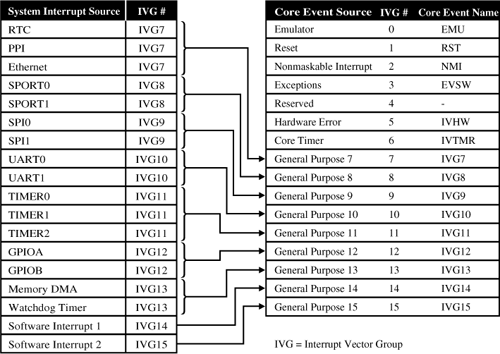
System level interrupts (those that are generated by peripherals) are handled in two stages—first in the system domain, and then in the core domain. Once the system interrupt controller (SIC) acknowledges an interrupt request from a peripheral, it compares the peripheral’s assigned priority to all current activity from other peripherals to decide when to service this particular interrupt request. The most important peripherals in an application should be mapped to the highest priority levels. In general, the highest bandwidth peripherals need the highest priority. One “exception” to this rule (pardon the pun!) is where an external processor or supervisory circuit uses a nonmaskable interrupt (NMI) to indicate the occurrence of an important event, such as powering down.
When the SIC is ready, it passes the interrupt request information to the core event controller (CEC), which handles all types of events, not just interrupts. Every interrupt from the SIC maps into a priority level at the CEC that regulates how to service interrupts with respect to one another, as Figure 7.3 shows. The CEC checks the “vector” assignment for the current interrupt request, to find the address of the appropriate interrupt service routine (ISR). Finally, it loads this address into the processor’s execution pipeline to start executing the ISR.
There are two key interrupt-related questions you need to ask when building your system. The first is, “How long does the processor take to respond to an interrupt?” The second is, “How long can any given task afford to wait when an interrupt comes in?”
The answers to these questions will determine what your processor can actually perform within an interrupt or exception handler.
For the purposes of this discussion, we define interrupt response time as the number of cycles it takes from when the interrupt is generated at the source (including the time it takes for the current instruction to finish executing) to the time that the first instruction is executed in the interrupt service routine. In our experience, the most common method software engineers use to evaluate this interval for themselves is to set up a programmable flag to generate an interrupt when its pin is triggered by an externally generated pulse.
The first instruction in the interrupt service routine then performs a write to a different flag pin. The resulting time difference is then measured on an oscilloscope. This method only provides a rough idea of the time taken to service interrupts, including the time required to latch an interrupt at the peripheral, propagate the interrupt through to the core, and then vector the core to the first instruction in the interrupt service routine. Thus, it is important to run a benchmark that more closely simulates the profile of your end application.
Once the processor is running code in an ISR, other higher priority interrupts are held off until the return address associated with the current interrupt is saved off to the stack. This is an important point, because even if you designate all other interrupt channels as higher priority than the currently serviced interrupt, these other channels will all be held off until you save the return address to the stack. The mechanism to re-enable interrupts kicks in automatically when you save the return address. When you program in C, any register the ISR uses will automatically be saved to the stack. Before exiting the ISR, the registers are restored from the stack. This also happens automatically, but depending on where your stack is located and how many registers are involved, saving and restoring data to the stack can take a significant amount of cycles.
Interrupt service routines often perform some type of processing. For example, when a line of video data arrives into its destination buffer, the ISR might run code to filter or down sample it. For this case, when the handler does the work, other interrupts are held off (provided that nesting is disabled) until the processor services the current interrupt.
When an operating system or kernel is used, however, the most common technique is to service the interrupt as soon as possible, release a semaphore, and perhaps make a call to a callback function, which then does the actual processing. The semaphore in this context provides a way to signal other tasks that it is okay to continue or to assume control over some resource.
For example, we can allocate a semaphore to a routine in shared memory. To prevent more than one task from accessing the routine, one task takes the semaphore while it is using the routine, and the other task has to wait until the semaphore has been relinquished before it can use the routine. A Callback Manager can optionally assist with this activity by allocating a callback function to each interrupt. This adds a protocol layer on top of the lowest layer of application code, but in turn it allows the processor to exit the ISR as soon as possible and return to a lower-priority task. Once the ISR is exited, the intended processing can occur without holding off new interrupts.
We already mentioned that a higher-priority interrupt could break into an existing ISR once you save the return address to the stack. However, some processors (like Blackfin) also support self-nesting of core interrupts, where an interrupt of one priority level can interrupt an ISR of the same level, once the return address is saved. This feature can be useful for building a simple scheduler or kernel that uses low-priority software-generated interrupts to preempt an ISR and allow the processing of ongoing tasks.
There are two additional performance-related issues to consider when you plan out your interrupt usage. The first is the placement of your ISR code. For interrupts that run most frequently, every attempt should be made to locate these in L1 instruction memory. On Blackfin processors, this strategy allows single-cycle access time. Moreover, if the processor were in the midst of a multicycle fetch from external memory, the fetch would be interrupted, and the processor would vector to the ISR code.
Keep in mind that before you re-enable higher priority interrupts, you have to save more than just the return address to the stack. Any register used inside the current ISR must also be saved. This is one reason why the stack should be located in the fastest available memory in your system. An L1 “scratchpad” memory bank, usually smaller in size than the other L1 data banks, can be used to hold the stack. This allows the fastest context switching when taking an interrupt.
It’s nice not to have to be an expert in your chosen processor, but even if you program in a high-level language, it’s important to understand certain things about the architecture for which you’re writing code.
One mandatory task when undertaking a signal-processing-intensive project is deciding what kind of programming methodology to use. The choice is usually between assembly language and a high-level language (HLL) like C or C++. This decision revolves around many factors, so it’s important to understand the benefits and drawbacks each approach entails.
The obvious benefits of C/C++ include modularity, portability, and reusability. Not only do the majority of embedded programmers have experience with one of these high-level languages, but also a huge code base exists that can be ported from an existing processor domain to a new processor in a relatively straightforward manner. Because assembly language is architecture-specific, reuse is typically restricted to devices in the same processor family. Also, within a development team it is often desirable to have various teams coding different system modules, and an HLL allows these cross-functional teams to be processor-agnostic.
One reason assembly has been difficult to program is its focus on actual data flow between the processor register sets, computational units and memories. In C/C++, this manipulation occurs at a much more abstract level through the use of variables and function/procedure calls, making the code easier to follow and maintain.
The C/C++ compilers available today are quite resourceful, and they do a great job of compiling the HLL code into tight assembly code. One common mistake happens when programmers try to “outsmart” the compiler. In trying to make it easier for the compiler, they in fact make things more difficult! It’s often best to just let the optimizing compiler do its job. However, the fact remains that compiler performance is tuned to a specific set of features that the tool developer considered most important. Therefore, it cannot exceed handcrafted assembly code performance in all situations.
The bottom line is that developers use assembly language only when it is necessary to optimize important processing-intensive code blocks for efficient execution. Compiler features can do a very good job, but nothing beats thoughtful, direct control of your application data flow and computation.
In order to achieve high performance media processing capability, you must understand the types of core processor structures that can help optimize performance. These include the following capabilities:
These features can make an enormous difference in computational efficiency. Let’s discuss each one in turn.
Processors are often benchmarked by how many millions of instructions they can execute per second (MIPS). However, for today’s processors, this can be misleading because of the confusion surrounding what actually constitutes an instruction. For example, multi-issue instructions, which were once reserved for use in higher-cost parallel processors, are now also available in low-cost, fixed-point processors. In addition to performing multiple ALU/MAC operations each core processor cycle, additional data loads, and stores can be completed in the same cycle. This type of construct has obvious advantages in code density and execution time.
An example of a Blackfin multi-operation instruction is shown in Figure 7.4. In addition to two separate MAC operations, a data fetch and data store (or two data fetches) can also be accomplished in the same processor clock cycle. Correspondingly, each address can be updated in the same cycle that all of the other activities are occurring.

Looping is a critical feature in real-time processing algorithms. There are two key looping-related features that can improve performance on a wide variety of algorithms: zero-overhead hardware loops and hardware loop buffers.
Zero-overhead loops allow programmers to initialize loops simply by setting up a count value and defining the loop bounds. The processor will continue to execute this loop until the count has been reached. In contrast, a software implementation would add overhead that would cut into the real-time processing budget.
Many processors offer zero-overhead loops, but hardware loop buffers, which are less common, can really add increased performance in looping constructs. They act as a kind of cache for instructions being executed in the loop. For example, after the first time through a loop, the instructions can be kept in the loop buffer, eliminating the need to re-fetch the same code each time through the loop. This can produce a significant savings in cycles by keeping several loop instructions in a buffer where they can be accessed in a single cycle. The use of the hardware loop construct comes at no cost to the HLL programmer, since the compiler should automatically use hardware looping instead of conditional jumps.
Let’s look at some examples to illustrate the concepts we’ve just discussed.
Allowing the processor to access multiple data words in a single cycle requires substantial flexibility in address generation. In addition to the more signal-processing-centric access sizes along 16- and 32-bit boundaries, byte addressing is required for the most efficient processing. This is important for multimedia processing because many video-based systems operate on 8-bit data. When memory accesses are restricted to a single boundary, the processor may spend extra cycles to mask off relevant bits.
Another beneficial addressing capability is circular buffering. For maximum efficiency, this feature must be supported directly by the processor, with no special management overhead. Circular buffering allows a programmer to define buffers in memory and stride through them automatically. Once the buffer is set up, no special software interaction is required to navigate through the data. The address generator handles nonunity strides and, more importantly, handles the “wraparound” feature illustrated in Figure 7.5. Without this automated address generation, the programmer would have to manually keep track of buffer pointer positions, thus wasting valuable processing cycles.
Example 7.5. Circular Buffer in Hardware

Base address and starting index address = 0x0
Index address register I0 points to address 0x0
Buffer length L = 44 (11 data elements * 4 bytes/element)
Modify register M0 = 16 (4 elements * 4 bytes/element)
Sample code:
R0 = [I0++M0]; // R0 = 1 and I0 points to 0x10 after execution R1 = [I0++M0]; // R1 = 5 and I0 points to 0x20 after execution R2 = [I0++M0]; // R2 = 9 and I0 points to 0x04 after execution R3 = [I0++M0]; // R3 = 2 and I0 points to 0x14 after execution R4 = [I0++M0]; // R4 = 6 and I0 points to 0x24 after execution |
Many optimizing compilers will automatically use hardware circular buffering when they encounter array addressing with a modulus operator.
An essential addressing mode for efficient signal-processing operations, such as the FFT and DCT, is bit reversal. Just as the name implies, bit reversal involves reversing the bits in a binary address. That is, the least significant bits are swapped in position with the most significant bits. The data ordering required by a radix-2 butterfly is in “bit-reversed” order, so bit-reversed indices are used to combine FFT stages. It is possible to calculate these bit-reversed indices in software, but this is very inefficient. An example of bit reversal address flow is shown in Figure 7.6.

Since bit reversal is very specific to algorithms like fast Fourier transforms and discrete Fourier transforms, it is difficult for any HLL compiler to employ hardware bit reversal. For this reason, comprehensive knowledge of the underlying architecture and assembly language are key to fully utilizing this addressing mode.
As processors increase in speed, it is necessary to add stages to the processing pipeline. For instances where a high-level language is the sole programming language, the compiler is responsible for dealing with instruction scheduling to maximize performance through the pipeline. That said, the following information is important to understand even if you’re programming in C.
On older processor architectures, pipelines are usually not interlocked. On these architectures, executing certain combinations of neighboring instructions can yield incorrect results. Interlocked pipelines like the one in Figure 7.7, on the other hand, make assembly programming (as well as the life of compiler engineers) easier by automatically inserting stalls when necessary. This prevents the assembly programmer from scheduling instructions in a way that will produce inaccurate results. It should be noted that, even if the pipeline is interlocked, instruction rearrangement could still yield optimization improvements by eliminating unnecessary stalls.

Let’s take a look at stalls in more detail. Stalls will show up for one of four reasons:
The instruction in question may itself take more than one cycle to execute. When this is the case, there isn’t anything you can do to eliminate the stall. For example, a 32-bit integer multiply might take three core-clock cycles to execute on a 16-bit processor. This will cause a “bubble” in two pipeline stages for a three-cycle instruction.
The second case involves the location of one instruction in the pipeline with respect to an instruction that follows it. For example, in some instructions, a stall may exist because the result of the first instruction is used as an operand of the following instruction. When this happens and you are programming in assembly, it is often possible to move the instruction so that the stall is not in the critical path of execution.
Here are some simple examples on Blackfin processors that demonstrate these concepts.
Register Transfer/Multiply latencies (One stall, due to R0 being used in the multiply):
R0 = R4; /* load R0 with contents of R4 */
<STALL>
R2.H = R1.L * R0.H; /* R0 is used as an operand */
In this example, any instruction that does not change the value of the operands can be placed in-between the two instructions to hide the stall.
When we load a pointer register and try to use the content in the next instruction, there is a latency of three stalls:
P3 = [SP++]; /* Pointer register loaded from stack */
<STALL>
<STALL>
<STALL>
R0 = P3; /* Use contents of P3 after it gets its value
   from earlier
The third case involves a change of flow. While a deeper pipeline allows increased clock speeds, any time a change of flow occurs, a portion of the pipeline is flushed, and this consumes core-clock cycles. The branching latency associated with a change of flow varies based on the pipeline depth. Blackfin’s 10-stage pipeline yields the following latencies:
The term “predicted” is used to describe what the sequencer does as instructions that will complete ten core-clock cycles later enter the pipeline. You can see that when the sequencer does not take a branch, and in effect “drops through” to the next instruction after the conditional one, there are no added cycles. When an unconditional branch occurs, the maximum number of stalls occurs (eight cycles). When the processor predicts that a branch occurs and it actually is taken, the number of stalls is four. In the case where it predicted no branch, but one is actually taken, it mirrors the case of an unconditional branch.
One more note here. The maximum number of stalls is eight, while the depth of the pipeline is ten. This shows that the branching logic in an architecture does not implicitly have to match the full size of the pipeline.
The last case involves a conflict when the processor is accessing the same memory space as another resource (or simply fetching data from memory other than L1). For instance, a core fetch from SDRAM will take multiple core-clock cycles. As another example, if the processor and a DMA channel are trying to access the same memory bank, stalls will occur until the resource is available to the lower-priority process.
Since the compiler’s foremost task is to create correct code, there are cases where the optimizer is too conservative. In these cases, providing the compiler with extra information (through pragmas, built-in keywords, or command-line switches) will help it create more optimized code.
In general, compilers can’t make assumptions about what an application is doing. This is why pragmas exist—to let the compiler know it is okay to make certain assumptions. For example, a pragma can instruct the compiler that variables in a loop are aligned and that they are not referenced to the same memory location. This extra information allows the compiler to optimize more aggressively, because the programmer has made a guarantee dictated by the pragma.
In general, a four-step process can be used to optimize an application consisting primarily of HLL code:
Compile with an HLL-optimizing compiler.
Profile the resulting code to determine the “hot spots” that consume the most processing bandwidth.
Update HLL code with pragmas, built-in keywords, and compiler switches to speed up the “hot spots.”
Replace HLL procedures/functions with assembly routines in places where the optimizer did not meet the timing budget.
For maximum efficiency, it is always a good idea to inspect the most frequently executed compiler-generated assembly code to make a judgment on whether the code could be more vectorized. Sometimes, the HLL program can be changed to help the compiler produce faster code through more use of multi-issue instructions. If this still fails to produce code that is fast enough, then it is up to the assembly programmer to fine-tune the code line-by-line to keep all available hardware resources from idling.
It is important to remember how the standard data types available in C actually map to the architecture you are using. For Blackfin processors, each type is shown in Table 7.2.
Table 7.2. C Data Types and Their Mapping to Blackfin Registers
C type | Blackfin equivalent |
|---|---|
char | 8-bit signed |
unsigned char | 8-bit unsigned |
short | 16-bit signed integer |
unsigned short | 16-bit unsigned integer |
int | 32-bit signed integer |
unsigned int | 32-bit unsigned integer |
long | 32-bit signed integer |
unsigned long | 32-bit unsigned integer |
The float(32-bit), double(32-bit), long long(64-bit) and unsigned long long (64-bit) formats are not supported natively by the processor, but these can be emulated.
We are often asked whether it is better to use arrays to represent data buffers in C, or whether pointers are better. Compiler performance engineers always point out that arrays are easier to analyze. Consider the example:
void array_example(int a[], ` b[], int sum[], int n)
{
      int i;
      for (i = 0; i < n; ++i)
      sum[i] = a[i] + b[i];
}
Even though we chose a simple example, the point is that these constructs are very easy to follow.
Now let’s look at the same function using pointers. With pointers, the code is “closer” to the processor’s native language.
void pointer_example( int a[], int b[], int sum[], int n) {
      int i;
      for (i = 0; i < n; ++i)
            *out++ = *a++ + *b++ ;
}
Which produces the most efficient code? Actually, there is usually very little difference. It is best to start by using the array notation because it is easier to read. An array format can be better for “alias” analysis in helping to ensure there is no overlap between elements in a buffer. If performance is not adequate with arrays (for instance, in the case of tight inner loops), pointers may be more useful.
Fixed-point processors often do not support division natively. Instead, they offer division primitives in the instruction set, and these help accelerate division.
The “cost” of division depends on the range of the inputs. There are two possibilities: You can use division primitives where the result and divisor each fit into 16 bits. On Blackfin processors, this results in an operation of ~40 cycles. For more precise, bitwise 32-bit division, the result is ~10x more cycles.
If possible, it is best to avoid division, because of the additional overhead it entails. Consider the example:
if ( X/Y > A/B )This can easily be rewritten as:
if ( X * B > A * Y )to eliminate the division.
Keep in mind that the compiler does not know anything about the data precision in your application. For example, in the context of the above equation rewrite, two 12-bit inputs are “safe,” because the result of the multiplication will be 24 bits maximum. This quick check will indicate when you can take a shortcut, and when you have to use actual division.
We already discussed hardware looping constructs. Here we’ll talk about software looping in C. We will attempt to summarize what you can do to ensure best performance for your application.
Try to keep loops short. Large loop bodies are usually more complex and difficult to optimize. Additionally, they may require register data to be stored in memory, decreasing code density and execution performance.
Avoid loop-carried dependencies. These occur when computations in the present iteration depend on values from previous iterations. Dependencies prevent the compiler from taking advantage of loop overlapping (i.e., nested loops).
Avoid manually unrolling loops. This confuses the compiler and cheats it out of a job at which it typically excels.
Don’t execute loads and stores from a noncurrent iteration while doing computations in the current loop iteration. This introduces loop-carried dependencies. This means avoiding loop array writes of the form:
for (i = 0; i < n; ++i)
    a[i] = b[i] * a[c[i]]; /* has array dependency*/
Make sure that inner loops iterate more than outer loops, since most optimizers focus on inner loop performance.
Avoid conditional code in loops. Large control-flow latencies may occur if the compiler needs to generate conditional jumps.
As an example,
for {
      if { ... } else {...}
    }
should be replaced, if possible, by:
if {
      for {...}
    } else {
      for   {...}
           }
Don’t place function calls in loops. This prevents the compiler from using hardware loop constructs, as we described earlier in this chapter.
Try to avoid using variables to specify stride values. The compiler may need to use division to figure out the number of loop iterations required, and you now know why this is not desirable!
It is important to think about how data is represented in your system. It’s better to pre-arrange the data in anticipation of “wider” data fetches—that is, data fetches that optimize the amount of data accessed with each fetch. Let’s look at an example that represents complex data.
One approach that may seem intuitive is:
short Real_Part[ N ];
short Imaginary_Part [ N ];
While this is perfectly adequate, data will be fetched in two separate 16-bit accesses. It is often better to arrange the array in one of the following ways:
short Complex [ N*2 ];
   or
 long Complex [ N ];
Here, the data can be fetched via one 32-bit load and used whenever it’s needed. This single fetch is faster than the previous approach.
On a related note, a common performance-degrading buffer layout involves constructing a 2D array with a column of pointers to malloc’d rows of data. While this allows complete flexibility in row and column size and storage, it may inhibit a compiler’s ability to optimize, because the compiler no longer knows if one row follows another, and therefore it can see no constant offset between the rows.
It is difficult for compilers to solve all of your problems automatically and consistently. This is why you should, if possible, avail yourself of “in-line” assembly instructions and intrinsics.
In-lining allows you to insert an assembly instruction into your C code directly. Sometimes this is unavoidable, so you should probably learn how to in-line for the compiler you’re using.
In addition to in-lining, most compilers support intrinsics, and their optimizers fully understand intrinsics and their effects. The Blackfin compiler supports a comprehensive array of 16-bit intrinsic functions, which must be programmed explicitly. Below is a simple example of an intrinsic that multiplies two 16-bit values.
# include <fract.h>
fract32 fdot( fract16 *x, fract16 *y, int n)
{
   fract32 sum = 0;
   int i;
   for (i = 0; i < n; i++)
      sum = add_fr1x32(sum, mult_fr1x32(x[i], y[i]));
   return sum;
}
Here are some other operations that can be accomplished through intrinsics:
Align operations
Packing operations
Disaligned loads
Unpacking
Quad 8-bit add/subtract
Dual 16-bit add/clip
Quad 8-bit average
Accumulator extract with addition
Subtract/absolute value/accumulate
The intrinsics that perform the above functions allow the compiler to take advantage of video-specific instructions that improve performance but that are difficult for a compiler to use natively.
When should you use in-lining, and when should you use intrinsics? Well, you really don’t have to choose between the two. Rather, it is important to understand the results of using both, so that they become tools in your programming arsenal. With regard to in-lining of assembly instructions, look for an option where you can include in the in-lining construct the registers you will be “touching” in the assembly instruction. Without this information, the compiler will invariably spend more cycles, because it’s limited in the assumptions it can make and therefore has to take steps that can result in lower performance. With intrinsics, the compiler can use its knowledge to improve the code it generates on both sides of the intrinsic code. In addition, the fact that the intrinsic exists means someone who knows the compiler and architecture very well has already translated a common function to an optimized code section.
The volatile data type is essential for peripheral-related registers and interrupt-related data.
Some variables may be accessed by resources not visible to the compiler. For example, they may be accessed by interrupt routines, or they may be set or read by peripherals.
The volatile attribute forces all operations with that variable to occur exactly as written in the code. This means that a variable is read from memory each time it is needed, and it’s written back to memory each time it’s modified. The exact order of events is preserved. Missing a volatile qualifier is the largest single cause of trouble when engineers port from one C-based processor to another. Architectures that don’t require volatile for hardware-related accesses probably treat all accesses as volatile by default and thus may perform at a lower performance level than those that require you to state this explicitly. When a C program works with optimization turned off but doesn’t work with optimization on, a missing volatile qualifier is usually the culprit.
Earlier we discussed the importance of an interlocked pipeline, but we also need to discuss the implications of the pipeline on the different operating domains of a processor. On Blackfin devices, there are two synchronization instructions that help manage the relationship between when the core and the peripherals complete specific instructions or sequences. While these instructions are very straightforward, they are sometimes used more than necessary. The CSYNC instruction prevents any other instructions from entering the pipeline until all pending core activities have completed. The SSYNC behaves in a similar manner, except that it holds off new instructions until all pending system actions have completed. The performance impact from a CSYNC is measured in multiple CCLK cycles, while the impact of an SSYNC is measured in multiple SCLKs. When either of these instructions is used too often, performance will suffer needlessly.
So when do you need these instructions? We’ll find out in a minute. But first we need to talk about memory transaction ordering.
Many embedded processors support the concept of a Load/Store data access mechanism. What does this mean, and how does it impact your application? “Load/Store” refers to the characteristic in an architecture where memory operations (loads and stores) are intentionally separated from the arithmetic functions that use the results of fetches from memory operations. The separation is made because memory operations, especially instructions that access off-chip memory or I/O devices, take multiple cycles to complete and would normally halt the processor, preventing an instruction execution rate of one instruction per core-clock cycle. To avoid this situation, data is brought into a data register from a source memory location, and once it is in the register, it can be fed into a computation unit.
In write operations, the “store” instruction is considered complete as soon as it executes, even though many clock cycles may occur before the data is actually written to an external memory or I/O location. This arrangement allows the processor to execute one instruction per clock cycle, and it implies that the synchronization between when writes complete and when subsequent instructions execute is not guaranteed. This synchronization is considered unimportant in the context of most memory operations. With the presence of a write buffer that sits between the processor and external memory, multiple writes can, in fact, be made without stalling the processor.
For example, consider the case where we write a simple code sequence consisting of a single write to L3 memory surrounded by five NOP (“no operation”) instructions. Measuring the cycle count of this sequence running from L1 memory shows that it takes six cycles to execute. Now let’s add another write to L3 memory and measure the cycle count again. We will see the cycle count increase by one cycle each time, until we reach the limits of the write buffer, at which point it will increase substantially until the write buffer is drained.
The relaxation of synchronization between memory accesses and their surrounding instructions is referred to as “weak ordering” of loads and stores. Weak ordering implies that the timing of the actual completion of the memory operations—even the order in which these events occur—may not align with how they appear in the sequence of a program’s source code.
In a system with weak ordering, only the following items are guaranteed:
Load operations will complete before a subsequent instruction uses the returned data.
Load operations using previously written data will use the updated values, even if they haven’t yet propagated out to memory.
Store operations will eventually propagate to their ultimate destination.
Because of weak ordering, the memory system is allowed to prioritize reads over writes. In this case, a write that is queued anywhere in the pipeline, but not completed, may be deferred by a subsequent read operation, and the read is allowed to be completed before the write. Reads are prioritized over writes because the read operation has a dependent operation waiting on its completion, whereas the processor considers the write operation complete, and the write does not stall the pipeline if it takes more cycles to propagate the value out to memory.
For most applications, this behavior will greatly improve performance. Consider the case where we are writing to some variable in external memory. If the processor performs a write to one location followed by a read from a different location, we would prefer to have the read complete before the write.
This ordering provides significant performance advantages in the operation of most memory instructions. However, it can cause side effects—when writing to or reading from nonmemory locations such as I/O device registers, the order of how read and write operations complete is often significant. For example, a read of a status register may depend on a write to a control register. If the address in either case is the same, the read would return a value from the write buffer rather than from the actual I/O device register, and the order of the read and write at the register may be reversed. Both of these outcomes could cause undesirable side effects. To prevent these occurrences in code that requires precise (strong) ordering of load and store operations, synchronization instructions like CSYNC or SSYNC should be used.
The CSYNC instruction ensures all pending core operations have completed and the core buffer (between the processor core and the L1 memories) has been flushed before proceeding to the next instruction. Pending core operations may include any pending interrupts, speculative states (such as branch predictions) and exceptions. A CSYNC is typically required after writing to a control register that is in the core domain. It ensures that whatever action you wanted to happen by writing to the register takes place before you execute the next instruction.
The SSYNC instruction does everything the CSYNC does, and more. As with CSYNC, it ensures all pending operations have to be completed between the processor core and the L1 memories. SSYNC further ensures completion of all operations between the processor core, external memory, and the system peripherals. There are many cases where this is important, but the best example is when an interrupt condition needs to be cleared at a peripheral before an interrupt service routine (ISR) is exited. Somewhere in the ISR, a write is made to a peripheral register to “clear” and, in effect, acknowledge the interrupt. Because of differing clock domains between the core and system portions of the processor, the SSYNC ensures the peripheral clears the interrupt before exiting the ISR. If the ISR were exited before the interrupt was cleared, the processor might jump right back into the ISR.
Load operations from memory do not change the state of the memory value itself. Consequently, issuing a speculative memory-read operation for a subsequent load instruction usually has no undesirable side effect. In some code sequences, such as a conditional branch instruction followed by a load, performance may be improved by speculatively issuing the read request to the memory system before the conditional branch is resolved.
For example,
IF CC JUMP away_from_here
RO = [P2];
...
away_from_here:
If the branch is taken, then the load is flushed from the pipeline, and any results that are in the process of being returned can be ignored. Conversely, if the branch is not taken, the memory will have returned the correct value earlier than if the operation were stalled until the branch condition was resolved.
However, this could cause an undesirable side effect for a peripheral that returns sequential data from a FIFO or from a register that changes value based on the number of reads that are requested. To avoid this effect, use an SSYNC instruction to guarantee the correct behavior between read operations.
Store operations never access memory speculatively, because this could cause modification of a memory value before it is determined whether the instruction should have executed.
We have already introduced several ways to use semaphores in a system. While there are many ways to implement a semaphore, using atomic operations is preferable, because they provide noninterruptible memory operations in support of semaphores between tasks.
The Blackfin processor provides a single atomic operation: TESTSET. The TESTSET instruction loads an indirectly addressed memory word, tests whether the low byte is zero, and then sets the most significant bit of the low memory byte without affecting any other bits. If the byte is originally zero, the instruction sets a status bit. If the byte is originally nonzero, the instruction clears the status bit. The sequence of this memory transaction is atomic—hardware bus locking insures that no other memory operation can occur between the test and set portions of this instruction. The TESTSET instruction can be interrupted by the core. If this happens, the TESTSET instruction is executed again upon return from the interrupt. Without something like this TESTSET facility, it is difficult to ensure true protection when more than one entity (for example, two cores in a dual-core device) vies for a shared resource.
Embedded media processors usually have a small amount of fast, on-chip memory, whereas microcontrollers usually have access to large external memories. A hierarchical memory architecture combines the best of both approaches, providing several tiers of memory with different performance levels. For applications that require the most determinism, on-chip SRAM can be accessed in a single core-clock cycle. Systems with larger code sizes can utilize bigger, higher-latency on-chip and off-chip memories.
Most complex programs today are large enough to require external memory, and this would dictate an unacceptably slow execution speed. As a result, programmers would be forced to manually move key code in and out of internal SRAM. However, by adding data and instruction caches into the architecture, external memory becomes much more manageable. The cache reduces the manual movement of instructions and data into the processor core, thus greatly simplifying the programming model.
Figure 7.8 demonstrates a typical memory configuration where instructions are brought in from external memory as they are needed. Instruction cache usually operates with some type of least recently used (LRU) algorithm, insuring that instructions that run more often get replaced less often. The figure also illustrates that having the ability to configure some on-chip data memory as cache and some as SRAM can optimize performance. DMA controllers can feed the core directly, while data from tables can be brought into the data cache as they are needed.

When porting existing applications to a new processor, “out-of-the-box” performance is important. As we saw earlier, there are many features compilers exploit that require minimal developer involvement. Yet, there are many other techniques that, with a little extra effort by the programmer, can have a big impact on system performance.
Proper memory configuration and data placement always pays big dividends in improving system performance. On high-performance media processors, there are typically three paths into a memory bank. This allows the core to make multiple accesses in a single clock cycle (e.g., a load and store, or two loads). By laying out an intelligent data flow, a developer can avoid conflicts created when the core processor and DMA vie for access to the same memory bank.
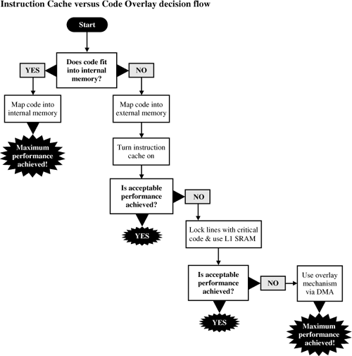
Maximum performance is only realized when code runs from internal L1 memory. Of course, the ideal embedded processor would have an unlimited amount of L1 memory, but this is not practical. Therefore, programmers must consider several alternatives to take advantage of the L1 memory that exists in the processor, while optimizing memory and data flows for their particular system. Let’s examine some of these scenarios.
The first, and most straightforward, situation is when the target application code fits entirely into L1 instruction memory. For this case, there are no special actions required, other than for the programmer to map the application code directly to this memory space. It thus becomes intuitive that media processors must excel in code density at the architectural level.
In the second scenario, a caching mechanism is used to allow programmers access to larger, less expensive external memories. The cache serves as a way to automatically bring code into L1 instruction memory as needed. The key advantage of this process is that the programmer does not have to manage the movement of code into and out of the cache. This method is best when the code being executed is somewhat linear in nature. For nonlinear code, cache lines may be replaced too often to allow any real performance improvement.
The instruction cache really performs two roles. For one, it helps pre-fetch instructions from external memory in a more efficient manner. That is, when a cache miss occurs, a cache-line fill will fetch the desired instruction, along with the other instructions contained within the cache line. This ensures that, by the time the first instruction in the line has been executed, the instructions that immediately follow have also been fetched. In addition, since caches usually operate with an LRU algorithm, instructions that run most often tend to be retained in cache.
Some strict real-time programmers tend not to trust cache to obtain the best system performance. Their argument is that if a set of instructions is not in cache when needed for execution, performance will degrade. Taking advantage of cache-locking mechanisms can offset this issue. Once the critical instructions are loaded into cache, the cache lines can be locked, and thus not replaced. This gives programmers the ability to keep what they need in cache and to let the caching mechanism manage less-critical instructions.
In a final scenario, code can be moved into and out of L1 memory using a DMA channel that is independent of the processor core. While the core is operating on one section of memory, the DMA is bringing in the section to be executed next. This scheme is commonly referred to as an overlay technique.
While overlaying code into L1 instruction memory via DMA provides more determinism than caching it, the trade-off comes in the form of increased programmer involvement. In other words, the programmer needs to map out an overlay strategy and configure the DMA channels appropriately. Still, the performance payoff for a well-planned approach can be well worth the extra effort.
The data memory architecture of an embedded media processor is just as important to the overall system performance as the instruction clock speed. Because multiple data transfers take place simultaneously in a multimedia application, the bus structure must support both core and DMA accesses to all areas of internal and external memory. It is critical that arbitration between the DMA controller and the processor core be handled automatically, or performance will be greatly reduced. Core-to-DMA interaction should only be required to set up the DMA controller, and then again to respond to interrupts when data is ready to be processed.
A processor performs data fetches as part of its basic functionality. While this is typically the least efficient mechanism for transferring data to or from off-chip memory, it provides the simplest programming model. A small, fast scratch pad memory is sometimes available as part of L1 data memory, but for larger, off-chip buffers, access time will suffer if the core must fetch everything from external memory. Not only will it take multiple cycles to fetch the data, but the core will also be busy doing the fetches.
It is important to consider how the core processor handles reads and writes. As we detailed above, Blackfin processors possess a multislot write buffer that can allow the core to proceed with subsequent instructions before all posted writes have completed. For example, in the following code sample, if the pointer register P0 points to an address in external memory and P1 points to an address in internal memory, line 50 will be executed before R0 (from line 46) is written to external memory:
...
Line 45: R0 =R1+R2;
Line 46: [P0] = R0; /* Write the value contained in R0 to slower
   external memory */
Line 47: R3 = 0x0 (z);
Line 48: R4 = 0x0 (z);
Line 49: R5 = 0x0 (z);
Line 50: [P1] = R0; /* Write the value contained in R0 to faster
   internal memory */
In applications where large data stores constantly move into and out of external DRAM, relying on core accesses creates a difficult situation. While core fetches are inevitably needed at times, DMA should be used for large data transfers, in order to preserve performance.
The flexibility of the DMA controller is a double-edged sword. When a large C/C++ application is ported between processors, a programmer is sometimes hesitant to integrate DMA functionality into already-working code. This is where data cache can be very useful, bringing data into L1 memory for the fastest processing. The data cache is attractive because it acts like a mini-DMA, but with minimal interaction on the programmer’s part.
Because of the nature of cache-line fills, data cache is most useful when the processor operates on consecutive data locations in external memory. This is because the cache doesn’t just store the immediate data currently being processed; instead, it prefetches data in a region contiguous to the current data. In other words, the cache mechanism assumes there’s a good chance that the current data word is part of a block of neighboring data about to be processed. For multimedia streams, this is a reasonable conjecture.
Since data buffers usually originate from external peripherals, operating with data cache is not always as easy as with instruction cache. This is due to the fact that coherency must be managed manually in “nonsnooping” caches. Nonsnooping means that the cache is not aware of when data changes in source memory unless it makes the change directly. For these caches, the data buffer must be invalidated before making any attempt to access the new data. In the context of a C-based application, this type of data is “volatile.” This situation is shown in Figure 7.9.

In the general case, when the value of a variable stored in cache is different from its value in the source memory, this can mean that the cache line is “dirty” and still needs to be written back to memory. This concept does not apply for volatile data. Rather, in this case the cache line may be “clean,” but the source memory may have changed without the knowledge of the core processor. In this scenario, before the core can safely access a volatile variable in data cache, it must invalidate (but not flush!) the affected cache line.
This can be performed in one of two ways. The cache tag associated with the cache line can be directly written, or a “Cache Invalidate” instruction can be executed to invalidate the target memory address. Both techniques can be used interchangeably, but the direct method is usually a better option when a large data buffer is present (e.g., one greater in size than the data cache size). The Invalidate instruction is always preferable when the buffer size is smaller than the size of the cache. This is true even when a loop is required, since the Invalidate instruction usually increments by the size of each cache line instead of by the more typical 1-, 2- or 4-byte increment of normal addressing modes.
From a performance perspective, this use of data cache cuts down on improvement gains, in that data has to be brought into cache each time a new buffer arrives. In this case, the benefit of caching is derived solely from the pre-fetch nature of a cache-line fill. Recall that the prime benefit of cache is that the data is present the second time through the loop.
One more important point about volatile variables, regardless of whether or not they are cached, if they are shared by both the core processor and the DMA controller, the programmer must implement some type of semaphore for safe operation. In sum, it is best to keep volatiles out of data cache altogether.
Let’s consider three widely used system configurations to shed some light on which approach works best for different system classifications.
This is perhaps the most popular system model, because media processors are often architected with this usage profile in mind. Caching the code alleviates complex instruction flow management, assuming the application can afford this luxury. This works well when the system has no hard real-time constraints, so that a cache miss would not wreak havoc on the timing of tightly coupled events (for example, video refresh or audio/video synchronization).
Also, in cases where processor performance far outstrips processing demand, caching instructions is often a safe path to follow, since cache misses are then less likely to cause bottlenecks. Although it might seem unusual to consider that an “oversized” processor would ever be used in practice, consider the case of a portable media player that can decode and play both compressed video and audio. In its audio-only mode, its performance requirements will be only a fraction of its needs during video playback. Therefore, the instruction/data management mechanism could be different in each mode.
Managing data through DMA is the natural choice for most multimedia applications, because these usually involve manipulating large buffers of compressed and uncompressed video, graphics, and audio. Except in cases where the data is quasi-static (for instance, a graphics icon constantly displayed on a screen), caching these buffers makes little sense, since the data changes rapidly and constantly. Furthermore, as discussed above, there are usually multiple data buffers moving around the chip at one time—unprocessed blocks headed for conditioning, partly conditioned sections headed for temporary storage, and completely processed segments destined for external display or storage. DMA is the logical management tool for these buffers, since it allows the core to operate on them without having to worry about how to move them around.
This approach is similar to the one we just described, except in this case part of L1 data memory is partitioned as cache, and the rest is left as SRAM for DMA access. This structure is very useful for handling algorithms that involve a lot of static coefficients or lookup tables. For example, storing a sine/cosine table in data cache facilitates quick computation of FFTs. Or, quantization tables could be cached to expedite JPEG encoding or decoding.
Keep in mind that this approach involves an inherent trade-off. While the application gains single-cycle access to commonly used constants and tables, it relinquishes the equivalent amount of L1 data SRAM, thus limiting the buffer size available for single-cycle access to data. A useful way to evaluate this trade-off is to try alternate scenarios (Data DMA/Cache versus only DMA) in a Statistical Profiler (offered in many development tools suites) to determine the percentage of time spent in code blocks under each circumstance.
In this scenario, data and code dependencies are so tightly intertwined that the developer must manually schedule when instruction and data segments move through the chip. In such hard real-time systems, determinism is mandatory, and thus cache isn’t ideal.
Although this approach requires more planning, the reward is a deterministic system where code is always present before the data needed to execute it, and no data blocks are lost via buffer overruns. Because DMA processes can link together without core involvement, the start of a new process guarantees that the last one has finished, so that the data or code movement is verified to have happened. This is the most efficient way to synchronize data and instruction blocks.
The Instruction/Data DMA combination is also noteworthy for another reason. It provides a convenient way to test code and data flows in a system during emulation and debug. The programmer can then make adjustments or highlight “trouble spots” in the system configuration.
An example of a system that might require DMA for both instructions and data is a video encoder/decoder. Certainly, video and its associated audio need to be deterministic for a satisfactory user experience. If the DMA signaled an interrupt to the core after each complete buffer transfer, this could introduce significant latency into the system, since the interrupt would need to compete in priority with other events. What’s more, the context switch at the beginning and end of an interrupt service routine would consume several core processor cycles. All of these factors interfere with the primary objective of keeping the system deterministic.
Figures 7.10 and 7.11 provide guidance in choosing between cache and DMA for instructions and data, as well as how to navigate the trade-off between using cache and using SRAM, based on the guidelines we discussed previously.

As a real-world illustration of these flowchart choices, Tables 7.3 and 7.4 provide actual benchmarks for G.729 and GSM AMR algorithms running on a Blackfin processor under various cache and DMA scenarios. You can see that the best performance can be obtained when a balance is achieved between cache and SRAM.
In short, there is no single answer as to whether cache or DMA should be the mechanism of choice for code and data movement in a given multimedia system. However, once developers are aware of the trade-offs involved, they should settle into the “middle ground,” the perfect optimization point for their system.
An MMU in a processor controls the way memory is set up and accessed in a system. The most basic capabilities of an MMU provides for memory protection, and when cache is used, it also determines whether or not a memory page is cacheable. Explicitly using the MMU is usually optional, because you can default to the standard memory properties on your processor.
On Blackfin processors, the MMU contains a set of registers that can define the properties of a given memory space. Using something called cacheability protection look-aside buffers (CPLBs), you can define parameters such as whether or not a memory page is cacheable, and whether or not a memory space can be accessed. Because the 32-bit-addressable external memory space is so large, it is likely that CPLBs will have to be swapped in and out of the MMU registers.
Because the amount of memory in an application can greatly exceed the number of available CPLBs, it may be necessary to use a CPLB manager. If so, it’s important to tackle some issues that could otherwise lead to performance degradation. First, whenever CPLBs are enabled, any access to a location without a valid CPLB will result in an exception being executed prior to the instruction completing. In the exception handler, the code must free up a CPLB and reallocate it to the location about to be accessed. When the processor returns from the exception handler, the instruction that generated the exception then executes.
If you take this exception too often, it will impact performance, because every time you take an exception, you have to save off the resources used in your exception handler. The processor then has to execute code to reprogram the CPLB. One way to alleviate this problem is to profile the code and data access patterns. Since the CPLBs can be “locked,” you can protect the most frequently used CPLBs from repeated page swaps.
Another performance consideration involves the search method for finding new page information. For example, a “nonexistent CPLB” exception handler only knows the address where an access was attempted. This information must be used to find the corresponding address “range” that needs to be swapped into a valid page. By locking the most frequently used pages and setting up a sensible search based on your memory access usage (for instructions and/or data), exception-handling cycles can be amortized across thousands of accesses.
A given MMU may also provide memory translation capabilities, enabling what’s known as virtual memory. This feature is controlled in a manner that is analogous to memory protection. Instead of CPLBs, translation look-aside buffers (TLBs) are used to describe physical memory space. There are two main ways in which memory translation is used in an application. As a holdover from older systems that had limited memory resources, operating systems would have to swap code in and out of a memory space from which execution could take place.
A more common use on today’s embedded systems still relates to operating system support. In this case, all software applications run thinking they are at the same physical memory space, when, of course, they are not. On processors that support memory translation, operating systems can use this feature to have the MMU translate the actual physical memory address to the same virtual address based on which specific task is running. This translation is done transparently, without the software application getting involved.
So far, we’ve seen that the compiler and assembler provide a bunch of ways to maximize performance on code segments in your system. Using of cache and DMA provide the next level for potential optimization. We will now review the third tier of optimization in your system—it’s a matter of physics.
Understanding the “physics” of data movement in a system is a required step at the start of any project. Determining if the desired throughput is even possible for an application can yield big performance savings without much initial investment.
For multimedia applications, on-chip memory is almost always insufficient for storing entire video frames. Therefore, the system must usually rely on L3 DRAM to support relatively fast access to large buffers. The processor interface to off-chip memory constitutes a major factor in designing efficient media frameworks, because access patterns to external memory must be well planned in order to guarantee optimal data throughput. There are several high-level steps that can ensure that data flows smoothly through memory in any system. Some of these are discussed below and play a key role in the design of system frameworks.
Accesses to external memory are most efficient when they are made in the same direction (e.g., consecutive reads or consecutive writes). For example, when accessing off-chip synchronous memory, 16 reads followed by 16 writes is always completed sooner than 16 individual read/write sequences. This is because a write followed by a read incurs latency. Random accesses to external memory generate a high probability of bus turnarounds. This added latency can easily halve available bandwidth. Therefore, it is important to take advantage of the ability to control the number of transfers in a given direction. This can be done either automatically (as we’ll see here) or by manually scheduling your data movements, which we’ll review.
A DMA channel garners access according to its priority, signified on Blackfin processors by its channel number. Higher priority channels are granted access to the DMA bus(es) first. Because of this, you should always assign higher priority DMA channels to peripherals with the highest data rates or with requirements for lowest latency.
To this end, MemDMA streams are always lower in priority than peripheral DMA activity. This is due to the fact that, with Memory DMA no external devices will be held off or starved of data. Since a Memory DMA channel requests access to the DMA bus as long as the channel is active, efficient use of any time slots unused by a peripheral DMA are applied to MemDMA transfers. By default, when more than one MemDMA stream is enabled and ready, only the highest priority MemDMA stream is granted.
When it is desirable for the MemDMA streams to share the available DMA bus bandwidth, however, the DMA controller can be programmed to select each stream in turn for a fixed number of transfers.
This “Direction Control” facility is an important consideration in optimizing use of DMA resources on each DMA bus. By grouping same-direction transfers together, it provides a way to manage how frequently the transfer direction changes on the DMA buses. This is a handy way to perform a first level of optimization without real-time processor intervention. More importantly, there’s no need to manually schedule bursts into the DMA streams.
When direction control features are used, the DMA controller preferentially grants data transfers on the DMA or memory buses that are going in the same read/write direction as in the previous transfer, until either the direction control counter times out, or until traffic stops or changes direction on its own. When the direction counter reaches zero, the DMA controller changes its preference to the opposite flow direction.
In this case, reversing direction wastes no bus cycles other than any physical bus turnaround delay time. This type of traffic control represents a trade-off of increased latency for improved utilization (efficiency). Higher block transfer values might increase the length of time each request waits for its grant, but they can dramatically improve the maximum attainable bandwidth in congested systems, often to above 90%.
Here’s an example that puts these concepts into some perspective:
As a rule of thumb, it is best to maximize same direction contiguous transfers during moderate system activity. For the most taxing system flows, however, it is best to select a block transfer value in the middle of the range to ensure no one peripheral gets locked out of accesses to external memory. This is especially crucial when at least two high-bandwidth peripherals (like PPIs) are used in the system.
In addition to using direction control, transfers among MDMA streams can be alternated in a “round-robin” fashion on the bus as the application requires. With this type of arbitration, the first DMA process is granted access to the DMA bus for some number of cycles, followed by the second DMA process, and then back to the first. The channels alternate in this pattern until all of the data is transferred. This capability is most useful on dual-core processors (for example, when both core processors have tasks that are awaiting a data stream transfer). Without this “round-robin” feature, the first set of DMA transfers will occur, and the second DMA process will be held off until the first one completes. Round-robin prioritization can help insure that both transfer streams will complete back-to-back.
Another thing to note: using DMA and/or cache will always help performance because these types of transactions transfer large data blocks in the same direction. For example, a DMA transfer typically moves a large data buffer from one location to another. Similarly, a cache-line fill moves a set of consecutive memory locations into the device, by utilizing block transfers in the same direction.
Buffering data bound for L3 in on-chip memory serves many important roles. For one, the processor core can access on-chip buffers for preprocessing functions with much lower latency than it can by going off-chip for the same accesses. This leads to a direct increase in system performance. Moreover, buffering this data in on-chip memory allows more efficient peripheral DMA access to this data. For instance, transferring a video frame on-the-fly through a video port and into L3 memory creates a situation where other peripherals might be locked out from accessing the data they need, because the video transfer is a high-priority process. However, by transferring lines incrementally from the video port into L1 or L2 memory, a Memory DMA stream can be initiated that will quietly transfer this data into L3 as a low-priority process, allowing system peripherals access to the needed data.
This concept will be further demonstrated in the “Performance-based Framework” later in this chapter.
Consider that on a Blackfin processor, core reads from L1 memory take one core-clock cycle, whereas core reads from SDRAM consume eight system clock cycles. Based on typical CCLK/SCLK ratios, this could mean that eight SCLK cycles equate to 40 CCLKs. Incidentally, these eight SCLKs reduce to only one SCLK by using a DMA controller in a burst mode instead of direct core accesses.
There is another point to make on this topic. For processors that have multiple data fetch units, it is better to use a dual-fetch instruction instead of back-to-back fetches. On Blackfin processors with a 32-bit external bus, a dual-fetch instruction with two 32-bit fetches takes nine SCLKs (eight for the first fetch and one for the second). Back-to-back fetches in separate instructions take 16 SCLKs (eight for each). The difference is that, in the first case, the request for the second fetch in the single instruction is pipelined, so it has a head start.
Similarly, when the external bus is 16 bits in width, it is better to use a 32-bit access rather than two 16-bit fetches. For example, when the data is in consecutive locations, the 32-bit fetch takes nine SCLKs (eight for the first 16 bits and one for the second). Two 16-bit fetches take 16 SCLKs (eight for each).
Each access to SDRAM can take several SCLK cycles, especially if the required SDRAM row has not yet been activated. Once a row is active, it is possible to read data from an entire row without reopening that row on every access. In other words, it is possible to access any location in memory on every SCLK cycle, as long as those locations are within the same row in SDRAM. Multiple SDRAM clock cycles are needed to close a row, and therefore constant row closures can severely restrict SDRAM throughput. Just to put this into perspective, an SDRAM page miss can take 20–50 CCLK cycles, depending on the SDRAM type.
Applications should take advantage of open SDRAM banks by placing data buffers appropriately and managing accesses whenever possible. Blackfin processors, as an example, keep track of up to four open SDRAM rows at a time, so as to reduce the setup time—and thus increase throughput—for subsequent accesses to the same row within an open bank. For example, in a system with one row open, row activation latency would greatly reduce the overall performance. With four rows open at one time, on the other hand, row activation latency can be amortized over hundreds of accesses.
Let’s look at an example that illustrates the impact this SDRAM row management can have on memory access bandwidth. Figure 7.12 shows two different scenarios of data and code mapped to a single external SDRAM bank. In the first case, all of the code and data buffers in external memory fit in a single bank, but because the access patterns of each code and data line are random, almost every access involves the activation of a new row. In the second case, even though the access patterns are randomly interspersed between code and data accesses, each set of accesses has a high probability of being within the same row. For example, even when an instruction fetch occurs immediately before and after a data access, two rows are kept open and no additional row activation cycles are incurred.
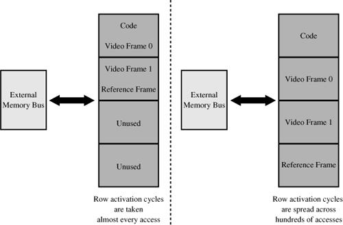
When we ran an MPEG-4 encoder from external memory (with both code and data in SDRAM), we gained a 6.5% performance improvement by properly spreading out the code and data in external memory.
External DRAM requires periodic refreshes to ensure that the data stored in memory retains its proper value. Accesses by the core processor or DMA engine are held off until an in-process refresh cycle has completed. If the refresh occurs too frequently, the processor can’t access SDRAM as often, and throughput to SDRAM decreases as a result.
On the Blackfin processor, the SDRAM Refresh Rate Control register provides a flexible mechanism for specifying the Auto-Refresh timing. Since the clock frequency supplied to the SDRAM can vary, this register implements a programmable refresh counter. This counter coordinates the supplied clock rate with the SDRAM device’s required refresh rate.
Once the desired delay (in number of SDRAM clock cycles) between consecutive refresh counter time-outs is specified, a subsequent refresh counter time-out triggers an Auto-Refresh command to all external SDRAM devices.
Not only should you take care not to refresh SDRAM too often, but also be sure you’re refreshing it often enough. Otherwise, stored data will start to decay because the SDRAM controller will not be able to keep corresponding memory cells refreshed.
Table 7.5 shows the impact of running with the best clock values and optimal refresh rates. Just in case you were wondering, RGB, CYMK, and YIQ are imaging/video formats. Conversion between the formats involves basic linear transformation that is common in video-based systems. Table 7.5 illustrates that the performance degradation can be significant with a nonoptimal refresh rate, depending on your actual access patterns. In this example, CCLK is reduced to run with an increased SCLK to illustrate this point. Doing this improves performance for this algorithm because the code fits into L1 memory and the data is partially in L3 memory. By increasing the SCLK rate, data can be fetched faster. What’s more, by setting the optimal refresh rate, performance increases a bit more.
Table 7.5. Using the Optimal Refresh Rate
Suboptimal SDRAM refresh rate | Optimal SDRAM refresh rate | |||
|---|---|---|---|---|
CCLK (MHz) | 594 MHz | 526 MHz | 526 MHz | |
SCLK (MHz) | 119 MHz | 132 MHz | 132 MHz | |
RGB to CMYK Conversion (iterations per second) | 226 | 244 | 250 | |
RGB to YIQ Conversion (iterations per second) | 266 | 276 | 282 | Total |
Cumulative Improvement | 5% | 2% | 7% | |
Another important consideration is the priority and arbitration schemes that regulate how processor subsystems behave with respect to one another. For instance, on Blackfin processors, the core has priority over DMA accesses, by default, for transactions involving L3 memory that arrive at the same time. This means that if a core read from L3 occurs at the same time a DMA controller requests a read from L3, the core will win, and its read will be completed first.
Let’s look at a scenario that can cause trouble in a real-time system. When the processor has priority over the DMA controller on accesses to a shared resource like L3 memory, it can lock out a DMA channel that also may be trying to access the memory. Consider the case where the processor executes a tight loop that involves fetching data from external memory. DMA activity will be held off until the processor loop has completed. It’s not only a loop with a read embedded inside that can cause trouble. Activities like cache line fills or nonlinear code execution from L3 memory can also cause problems because they can result in a series of uninterruptible accesses.
There is always a temptation to rely on core accesses (instead of DMA) at early stages in a project, for a number of reasons. The first is that this mimics the way data is accessed on a typical prototype system. The second is that you don’t always want to dig into the internal workings of DMA functionality and performance. However, with the core and DMA arbitration flexibility, using the memory DMA controller to bring data into and out of internal memory gives you more control of your destiny early on in a project. We will explore this concept in more detail in the following section.
As more applications transition from PC-centric designs to embedded solutions, software engineers need to port media-based algorithms from prototype systems where memory is an “unlimited” resource (such as a PC or a workstation) to embedded systems where resource management is essential to meet performance requirements. Ideally, they want to achieve the highest performance for a given application without increasing the complexity of their “comfortable” programming model. Figure 7.13 shows a summary of the challenges they face in terms of power consumption, memory allocation, and performance.
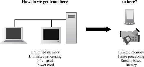
A small set of programming frameworks are indispensable in navigating through key challenges of multimedia processing, like organizing input and output data buffer flows, partitioning memory intelligently, and using semaphores to control data movement. While reading this chapter, you should see how the concepts discussed in the previous chapters fit together into a cohesive structure. Knowing how audio and video work within the memory and DMA architecture of the processor you select will help you build your own framework for your specific application.
Typically, a project starts out with a prototype developed in a high-level language such as C, or in a simulation and modeling tool such as Matlab or LabView. This is a particularly useful route for a few reasons. First, it’s easy to get started, both psychologically and materially. Test data files, such as video clips or images, are readily available to help validate an algorithm’s integrity. In addition, no custom hardware is required, so you can start development immediately, without waiting for, and debugging, a test setup. Optimal performance is not a focus at this stage because processing and memory resources are essentially unlimited on a desktop system. Finally, you can reuse code from other projects as well as from specialized toolbox packages or libraries.
The term “framework” has a wide variety of meanings, so let’s define exactly what we mean by the word. It’s important to harness the memory system architecture of an embedded processor to address performance and capacity trade-offs in ways that enable system development. Unfortunately, if we were to somehow find embedded processors with enough single-cycle memory to fit complicated systems on-chip, the cost and power dissipation of the device would be prohibitive. As a result, the embedded processor needs to use internal and external memory in concert to construct an application.
To this end, “framework” is the term we use to describe the complete code and data movement infrastructure within the embedded system. If you’re working on a prototype development system, you can access data as if it were in L1 memory all of the time. In an embedded system, however, you need to choreograph data movement to meet the required real-time budget. A framework specifies how data moves throughout the system, configuring and managing all DMA controllers and related descriptors. In addition, it controls interrupt management and the execution of the corresponding interrupt service routines. Code movement is an integral part of the framework. We’ll soon review some examples that illustrate how to carefully place code so that it peacefully coexists with the data movement tasks.
So, the first deliverable to tackle on an embedded development project is defining the framework. At this stage of the project, it is not necessary to integrate the actual algorithm yet. Your project can start off on the wrong foot if you add the embedded algorithm before architecting the basic data and coding framework!
There are many important questions to consider when defining your framework. Hopefully, by answering these questions early in the design process, you’ll be able to avoid common tendencies that could otherwise lead you down the wrong design path.
We have already covered most of these topics in previous chapters, and it is important to reexamine these items before you lay out your own framework. We will now attack a fundamental issue related to the above questions: understanding your worst-case situation in the application timeline.
Before starting to code your algorithm, you need to identify the timeline requirements for the smallest processing interval in your application. This is best characterized as the minimum time between data collection intervals. In a video-based system, this interval typically relates to a macroblock within an image, a line of video data, or perhaps an entire video frame. The processor must complete its task on the current buffer before the next data set overwrites the same buffer. In some applications, the processing task at hand will simply involve making a decision on the incoming data buffer. This case is easier to handle because the processed data does not have to be transferred out. When the buffer is processed and the results still need to be stored or displayed, the processing interval calculation must include the data transfer time out of the system as well.
Figure 7.14 shows a summary of the minimum timelines associated with a variety of applications. The timeline is critical to understand because in the end, it is the foremost benchmark that the processor must meet.

An NTSC-based application that processes data on a frame-by-frame basis takes 33 ms to collect a frame of video. Let’s assume that at the instant the first frame is received, the video port generates an interrupt. By the time the processor services the interrupt, the beginning of the next frame is already entering the FIFO of the video port. Because the processor needs to access one buffer while the next is on its way in, a second buffer needs to be maintained. Therefore, the time available to process the frame is 33 ms. Adding additional buffers can help to some extent, but if your data rates overwhelm your processor, this only provides short-term relief.
When selecting a processor, it’s easy to oversimplify the estimates for overall bandwidth required. Unfortunately, this mistake is often realized after a processor has been chosen, or after the development schedule has been approved by management!
Consider the viewfinder subsystem of a digital video camera. Here, the raw video source feeds the input of the processor’s video port. The processor then down samples the data, converts the color space from YCbCr to RGB, packs each RGB word into a 16-bit output, and sends it to the viewfinder’s LCD. The process is shown in Figure 7.15.
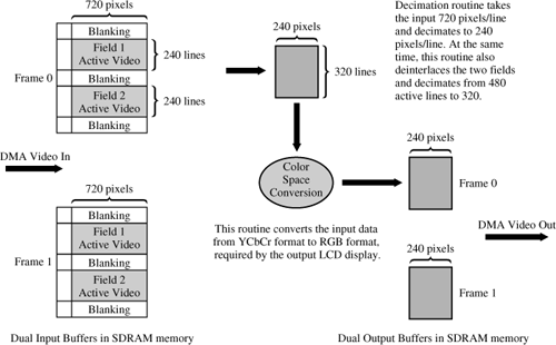
The system described above provides a good platform to discuss design budgets within a framework. Given a certain set of data flows and computational routines, how can we determine if the processor is close to being “maxed out”?
Let’s assume here we’re using a single processor core running at 600 MHz, and the video camera generates NTSC video at the rate of 27 Mbytes per second.
So the basic algorithm flow is:
Read in an NTSC frame of input data (1716 bytes/row × 525 rows).
Down sample it to a QVGA image containing (320 × 240 pixels) × (2 bytes/ pixel).
Convert the data to RGB format.
Add a graphics overlay, such as the time of day or an “image tracker” box.
Send the final output buffer to the QVGA LCD at its appropriate refresh rate.
We’d like to get a handle on the overall performance of this algorithm. Is it taxing the processor too much, or barely testing it? Do we have room left for additional video processing, or for higher input frame rates or resolutions?
In order to measure the performance of each step, we need to gather timing data. It’s convenient to do this with a processor’s built-in cycle counters, which use the core-clock (CCLK) as a time base. Since in our example CCLK = 600 MHz, each tick of the cycle counter measures 1/(600 MHz), or 1.67 ns.
OK, so we’ve done our testing, and we find the following:
Step A: (27 million cycles per second/30 frames per second), or 900,000 cycles to collect a complete frame of video.
Steps B/C: 5 million
CCLKcycles to down sample and color-convert that frame.Steps D/E: 11 million
CCLKcycles to add a graphics overlay and send that one processed frame to the LCD panel.
Keep in mind that these processes don’t necessarily happen sequentially. Instead, they are pipelined for efficient data flow. But measuring them individually gives us insight into the ultimate limits of the system.
Given these timing results, we might be misled into thinking, “Wow, it only takes 5 million CCLK cycles to process a frame (because all other steps are allocated to the inputting and outputting of data), so 30 frames per second would only use up about 30 × 5 = 150 MHz of the core’s 600 MHz performance. We could even do 60 frames/sec and still have 50% of the processor bandwidth left.”
This type of surface analysis belies the fact that there are actually three important bandwidth studies to perform in order to truly get your hands around a system:
Bottlenecks in any one of these can prevent your application from working properly. More importantly, the combined bandwidth of the overall system can be very different than the sum of each individual bandwidth number, due to interactions between resources.
In our example, in Steps B and C the processor core needs to spend 5 M cycles operating on the input buffer from Step A. However, this analysis does not account for the total time available for the core to work on each input buffer. In processor cycles, a 600 MHz core can afford to spend around 20 M cycles (600 MHz/30 fps) on each input frame of data, before the next frame starts to arrive.
Viewed from this angle, then, Steps B and C tell us that the processor core is 5 M/20 M, or 25%, loaded. That’s a far cry from the “intuitive” ratio of 5 M/600 M, or 0.8%, but it’s still low enough to allow for a considerable amount of additional processing on each input buffer.
What would happen if we doubled the frame rate to 60 frames/second, keeping the identical resolution? Even though there are twice as many frames, it would still take only 5 M cycles to do the processing of Steps B and C, since the frame size has not changed. But now our 600 MHz core can only afford to spend 10 M cycles (600 MHz/60 frames/sec) on each input frame. Therefore, the processor is 50% loaded (5 M processing cycles/10 M available cycles) in this case.
Taking a different slant, let’s dial back the frame rate to 30 frames/sec, but double the resolution of each frame. Effectively, this means there are twice as many pixels per frame. Now, it should take twice as long to read in a single frame and twice as long (10 M cycles) to process each frame as in the last case. However, since there are only 30 frames/second, If CCLK remains at 600 MHz, then the core can afford to spend 20 M cycles on each frame. As in the last case, the processor is 50% loaded (10 M processing cycles/20 M available cycles). It’s good to see that these last two analyses matched up, since the total input data rate is identical.
Let’s forget about the processor core for a minute and concentrate on the DMA controller. On a dual-core Blackfin processor, each 32-bit peripheral DMA channel (such as one used for video in/out functionality) can transfer data at clock speeds up to half the system clock (SCLK) rate, where SCLK maxes out at 133 MHz. This means that a given DMA channel can transfer data on every other SCLK cycle. Other DMA channels can use the free slots on a given DMA bus. In fact, for transfers in the same direction (e.g., into or out of the same memory space), every bus cycle can be utilized. For example, if the video port (PPI) is transferring data from external memory, the audio port (SPORT) can interleave its transfers from external memory to an audio codec without spending a cycle of latency for turning around the bus.
This implies that the maximum bandwidth on a given DMA bus is 133 MHz × 4 bytes, or 532 Mbytes/sec. As an aside, keep in mind that a processor might have multiple DMA buses available, thus allowing multiple transfers to occur at the same time.
In an actual system, however, it is not realistic to assume every transfer will occur in the same direction. Practically speaking, it is best to plan on a maximum transfer rate of one half of the theoretical bus bandwidth. This bus “derating” is important in an analogous manner to that of hardware component selection. In any system design, the more you exceed a 50% utilization factor, the more care you must take during software integration and future software maintenance efforts. If you plan on using 50% from the beginning, you’ll leave yourself plenty of breathing room for coping with interactions of the various DMA channels and the behavior of the memory to which you’re connecting. Of course, this value is not a hard limit, as many systems exist where every cycle is put to good use. The 50% derating factor is simply a useful guideline to allow for cycles that may be lost from bus turnarounds or DMA channel conflicts.
Planning the memory access patterns in your application can mean the difference between crafting a successful project and building a random number generator! Determining up front if the desired throughput is even possible for an application can save lots of headaches later.
As a system designer, you’ll need to balance memory of differing sizes and performance levels at the onset of your project.
For multimedia applications involving image sizes above QCIF (176 × 144 pixels), on-chip memory is almost always insufficient for storing entire video frames. Therefore, the system must rely on L3 DRAM to support relatively fast access to large buffers. The processor interface to off-chip memory constitutes a major factor in designing efficient media frameworks, because access patterns to external memory must be well thought out in order to guarantee optimal data throughput. There are several high-level steps to ensure that data flows smoothly through memory in any system.
Once you understand the actual bandwidth needs for the processor, DMA and memory components, you can return to the issue at hand: what is the minimum processing interval that needs to be satisfied in your application?
Let’s consider a new example where the smallest collection interval is defined to be a line of video. Determining the processing load under ideal conditions (when all code and data are in L1 memory) is easy. In the case where we are managing two buffers at a time, we must look at the time it takes to fill each buffer. The DMA controller “ping-pongs” between buffers to prevent a buffer from being overwritten while processing is underway on it. While the computation is done “in place” in Buffer 0, the peripheral fills Buffer 1. When Buffer 1 fills, Buffer 0 again becomes the destination. Depending on the processing timeline, an interrupt can optionally signal when each buffer has been filled.
So far, everything seems relatively straightforward. Now, consider what happens when the code is not in internal memory, but instead is executing from external memory. If instruction cache is enabled to improve performance, a fetch to external memory will result in a cache-line fill whenever there is not a match in L1 instruction memory (i.e., a cache-line miss occurs). The resulting fill will typically return at least 32 bytes. Because a cache-line fill is not interruptible—once it starts, it continues to completion—all other accesses to external memory are held off while it completes. From external memory, a cache-line fill can result in a fetch that takes 8 SCLKs (on Blackfin processors) for the first 32-bit word, followed by 7 additional SCLKs for the next seven 32-bit fetches (1 SCLK for each 32-bit fetch). This may be okay when the code being brought in is going to be executed. But now, what if one of the instructions being executed is a branch instruction, and this instruction, in turn, also generates a cache-line miss because it is more than a cache-line fill width away in memory address space? Code that is fetched from the second cache-line fill might also contain dual accesses that again are both data cache misses. What if these misses result in accesses to a page in external memory that is not active? Additional cycles can continue to hold off the competing resources. In a multimedia system, this situation can cause clicking sounds or video artifacts.
By this time, you should see the snowballing effect of the many factors that can reduce the performance of your application if you don’t consider the interdependence of every framework component. Figure 7.16 illustrates one such situation.

The scenario described in Figure 7.16 demonstrates the need to, from the start, plan the utilization on the external bus. Incidentally, it is this type of scenario that drives the need for FIFOs in media processor peripherals, to insure that each interface has a cushion against the occurrence of these hard-to-manage system events. When you hear a click or see a glitch, what may be happening is that one of the peripherals has encountered an overrun (when it is receiving) or underrun (when it is transmitting) condition. It is important to set up error interrupt service routines to trap these conditions. This sounds obvious, but it’s an often overlooked step that can save loads of debugging time.
The question is, what kinds of tasks will happen at the worst possible point in your application? In the scenario we just described with multiple cache-line fills happening at the wrong time, eliminating cache may solve the problem on paper, but if your code will not fit into L1 memory, you will have to decide between shutting off cache and using the available DMA channels to manage code and data movement into and out of L1 memory. Even when system bandwidth seems to meet your initial estimates, the processor has to be able to handle the ebbs and flows of data transfers for finite intervals in any set of circumstances.
So far we’ve defaulted to talking about single-core processors for embedded media applications. However, there’s a lot to be said about dual-core approaches. A processor with two cores (or more, if you’re really adventurous) can be very powerful, yet along with the extra performance can come an added measure of complexity. As it turns out, there are a few common and quite useful programming models that suit a dual-core processor, and we’ll examine them here.
There are two types of dual-core architectures available today. The first we’ll call an “asymmetric” dual-core processor, meaning that the two cores are architecturally different. This means that, in addition to possessing different instruction sets, they also run at different operating frequencies and have different memory and programming models.
The main advantage of having two different architectures in the same physical package is that each core can optimize a specific portion of the processing task. For example, one core might excel at controller functionality, while the second one might target higher-bandwidth processing.
As you may figure, there are several disadvantages with asymmetric arrangements. For one, they require two sets of development tools and two sets of programming skill sets in order to build an application. Secondly, unused processing resources on one core are of little use to a fully loaded second core, since their competencies are so divergent. What’s more, asymmetric processors make it difficult to scale from light to heavy processing profiles. This is important, for instance, in battery-operated devices, where frequency and voltage may be adjusted to meet real-time processing requirements; asymmetric cores don’t scale well because the processing load is divided unevenly, so that one core might still need to run at maximum frequency while the other could run at a much lower clock rate. Finally, as we will see, asymmetric processors don’t support many different programming models, which limits design options (and makes them much less exciting to talk about!).
In contrast to the asymmetric processor, a symmetric dual-core processor (extended to “symmetric multiprocessor,” or SMP) consists of two identical cores integrated into a single package. The dual-core Blackfin ADSP-BF561 is a good example of this device class. An SMP requires only a single set of development tools and a design team with a single architectural knowledge base. Also, since both cores are equivalent, unused processing resources on one core can often be leveraged by the other core. Another very important benefit of the SMP architecture is the fact that frequency and voltage can more easily be modified together, improving the overall energy usage in a given application. Lastly, while the symmetric processor supports an asymmetric programming model, it also supports many other models that are very useful for multimedia applications.
The main challenge with the symmetric multiprocessor is splitting an algorithm across two processor cores without complicating the programming model.
There are several basic programming models that designers employ across a broad range of applications. We described an asymmetric processor in the previous discussion; we will now look at its associated programming model.
The traditional use of an asymmetric dual-core processor involves discrete and often different tasks running on each of the cores, as shown in Figure 7.17. For example, one of the cores may be assigned all of the control-related tasks. These typically include graphics and overlay functionality, as well as networking stacks and overall flow control. This core is also most often where the operating system or kernel will reside. Meanwhile, the second core can be dedicated to the high-intensity processing functions of the application. For example, compressed data may come over the network into the first core. Received packets can feed the second core, which in turn might perform some audio and video decode function.

In this model, the two processor cores act independently from each other. Logically, they are more like two stand-alone processors that communicate through the interconnect structures between them. They don’t share any code and share very little data. We refer to this as the Asymmetric Programming Model. This model is preferred by developers who employ separate teams in their software development efforts. The ability to allocate different tasks to different processors allows development to be accomplished in parallel, eliminating potential critical path dependencies in the project. This programming model also aids the testing and validation phases of the project. For example, if code changes on one core, it does not necessarily invalidate testing efforts already completed on the other core.
Also, by having a dedicated processor core available for a given task, code developed on a single-core processor can be more easily ported to “half” of the dual-core processor. Both asymmetric and symmetric multiprocessors support this programming model. However, having identical cores available allows for the possibility of re-allocating any unused resources across functions and tasks. As we described earlier, the symmetric processor also has the advantage of providing a common, integrated environment.
Another important consideration of this model relates to the fact that the size of the code running the operating system and control tasks is usually measured in megabytes. As such, the code must reside in external memory, with instruction cache enabled. While this scheme is usually sufficient, care must be taken to prevent cache line fills from interfering with the overall timeline of the application. A relatively small subset of code runs the most often, due to the nature of algorithm coding. Therefore, enabling instruction cache is usually adequate in this model.
Because there are two identical cores in a symmetric multiprocessor, traditional processing-intensive applications can be split equally across each core. We call this a Homogeneous Model. In this scheme, code running on each core is identical. Only the data being processed is different. In a streaming multichannel audio application, for example, this would mean that one core processes half of the audio channels, and the other core processes the remaining half. Extending this concept to video and imaging applications, each core might process alternate frames. This usually translates to a scenario where all code fits into internal memory, in which case instruction cache is probably not used.
The communication flow between cores in this model is usually pretty basic. A mailbox interrupt (or on the Blackfin processor, a supplemental interrupt between cores) can signal the other core to check for a semaphore, to process new data or to send out processed data. Usually, an operating system or kernel is not required for this model; instead, a “super loop” is implemented. We use the term “super loop” to indicate a code segment that just runs over and over again, of the form:
While (1)
      {
      Process_data();
      Send_results();
      Idle();
}In the Master-Slave usage model, both cores perform intensive computation in order to achieve better utilization of the symmetric processor architecture. In this arrangement, one core (the master) controls the flow of the processing and actually performs at least half the processing load. Portions of specific algorithms are split and handled by the slave, assuming these portions can be parallelized. This situation is represented in Figure 7.18.
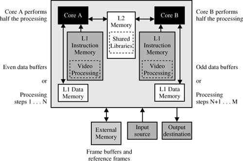
A variety of techniques, among them interrupts and semaphores, can be used to synchronize the cores in this model. The slave processor usually takes less processing time than the master does. Thus, the slave can poll a semaphore in shared memory when it is ready for more work. This is not always a good idea, though, because if the master core is still accessing the bus to the shared memory space, a conflict will arise. A more robust solution is for the slave to place itself in idle mode and wait for the master to interrupt it with a request to perform the next block of work.
A scheduler or simple kernel is most useful in this model, as we’ll discuss later in the chapter.
Also depicted in Figure 7.18, a variation on the Master-Slave model allocates processing steps to each core. That is, one core is assigned one or more serial steps, and the other core handles the remaining ones. This is analogous to a manufacturing pipeline where one core’s output is the next core’s input. Ideally, if the processing task separation is optimized, this will achieve a performance advantage greater than that of the other models. The task separation, however, is heavily dependent on the processor architecture and its memory hierarchy. For this reason, the Pipelined Model isn’t as portable across processors as the other programming models are.
As Table 7.6 illustrates, the symmetric processor supports many more programming models than the asymmetric processor does, so you should consider all of your options before starting a project!
We have discussed how tasks can be allocated across multiple cores when necessary. We have also described the basic ways a programming model can take shape. We are now ready to discuss several types of multimedia frameworks that can ride on top of either a single or dual-core processor. Regardless of the programming model, a framework is necessary in all but the simplest applications.
While they represent only a subset of all possible strategies, the categories shown below provide a good sampling of the most popular resource management situations. For illustration, we’ll continue to use video-centric systems as a basis for these scenarios, because they incorporate the transfer of large amounts of data between internal and external memory, as well as the movement of raw data into the system and processed data out of the system. Here are the categories we will explore:
A system where data is processed as it is collected
A system where programming ease takes precedence over performance
A processor-intensive application where performance supersedes programming ease
We’ll first discuss systems where data is processed on-the-fly, as it is collected. Two basic categories of this class exist: low “system latency” applications and systems with either no external memory or a reduced external memory space.
This scenario strives for the absolute lowest system latency between input data and output result. For instance, imagine the camera-based automotive object avoidance system of Figure 7.19 tries to minimize the chance of a collision by rapidly evaluating successive video frames in the area of view. Because video frames require a tremendous amount of storage capacity (recall that one NTSC active video frame alone requires almost 700 Kbytes of memory), they invariably need external memory for storage. But if the avoidance system were to wait until an entire road image were buffered into memory before starting to process the input data, 33 ms of valuable time would be lost (assuming a 30-Hz frame rate). This is in contrast to the time it takes to collect a single line of data, which is only 63 μs.
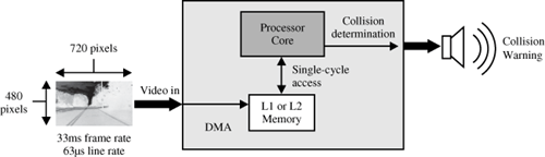
To ensure lowest latency, video can enter L1 or L2 memory for processing on a line-by-line basis, rendering quick computations that can lead to quicker decisions. If the algorithm operates on only a few lines of video at a time, the frame storage requirements are much less difficult to meet. A few lines of video can easily fit into L2 memory, and since L2 memory is closer to the core processor than off-chip DRAM, this also improves performance considerably when compared to accessing off-chip memory.
Under this framework, the processor core can directly access the video data in L1 or L2 memory. In this fashion, the programming model matches the typical PC-based paradigm. In order to guarantee data integrity, the software needs to insure that the active video frame buffer is not overwritten with new data until processing on the current frame completes. As shown in Figure 7.20, this can be easily managed through a “ping-pong” buffer, as well through the use of a semaphore mechanism. The DMA controller in this framework is best configured in a descriptor mode, where Descriptor 0 points to Descriptor 1 when its corresponding data transfer completes. In turn, Descriptor 1 points back to Descriptor 0. This looks functionally like an Autobuffer scheme, which is also a realistic option to employ. What happens when the processor is accessing a buffer while it is being output to a peripheral? In a video application, you will most likely see some type of smearing between frames. This will show up as a blurred image, or one that appears to jump around.

In our collision-avoidance system, the result of processing each frame is a decision—is a crash imminent or not? Therefore, in this case there is no output display buffer that needs protection against being overwritten. The size of code required for this type of application most likely will support execution from on-chip memory. This is helpful—again, it’s one less thing to manage.
In this example, the smallest processing interval is the time it takes to collect a line of video from the camera. There are similar applications where multiple lines are required—for example, a 3 × 3 convolution kernel for image filtering.
Not all of the applications that fit this model have low system-latency requirements. Processing lines on-the-fly is useful for other situations as well. JPEG compression can lend itself to this type of framework, where image buffering is not required because there is no motion component to the compression. Here, macroblocks of 16 pixels × 16 pixels form a compression work unit. If we double-buffer two sets of 16 active-video lines, we can have the processor work its way through an image as it is generated. Again, a double-buffer scheme can be set up where two sets of 16 lines are managed. That is, one set of 16 lines is compressed while the next set is transferred into memory.
The second framework we’ll discuss focuses entirely on using the simplest programming model at the possible expense of some performance. In this scenario, time to market is usually the most important factor. This may result in overspecifying a device, just to be sure there’s plenty of room for inefficiencies caused by nonoptimal coding or some small amount of redundant data movements. In reality, this strategy also provides an upgrade platform, because processor bandwidth can ultimately be freed up once it’s possible to focus on optimizing the application code. A simple flow diagram is shown in Figure 7.21.

We used JPEG as an example in the previous framework because no buffering was required. For this framework any algorithm that operates on more than one line of data at a time, and is not an encoder or decoder, is a good candidate. Let’s say we would like to perform a 3 × 3 two-dimensional convolution as part of an edge detection routine. For optimal operation, we need to have as many lines of data in internal memory as possible. The typical kernel navigates from left to right across an image, and then starts at the left side again (the same process used when reading words on a page). This convolution path continues until the kernel reaches the end of the entire image frame.
It is very important for the DMA controller to always fetch the next frame of data while the core is crunching on the current frame. That said, care should be taken to insure that DMA can’t get too far ahead of the core, because then unprocessed data would be overwritten. A semaphore mechanism is the only way to guarantee that this process happens correctly. It can be provided as part of an operating system or in some other straightforward implementation.
Consider that, by the time the core finishes processing its first subframe of data, the DMA controller either has to wrap back around to the top of the buffer, or it has to start filling a second buffer. Due to the nature of the edge detection algorithm, it will most certainly require at least two buffers. The question is, is it better to make the algorithm library aware of the wrap-around, or to manage the data buffer to hide this effect from the library code?
The answer is, it is better not to require changes to an algorithm that has already been tested on another platform. Remember, on a C-based application on the PC, you might simply pass a pointer to the beginning of an image frame in memory when it is available for processing. The function may return a pointer to the processed buffer.
On an embedded processor, that same technique would mean operating on a buffer in external memory, which would hurt performance. That is, rather than operations at 30 frames per second, it could mean a maximum rate of just a few frames per second. This is exactly the reason to use a framework that preserves the programming model and achieves enough performance to satisfy an application’s needs, even if requirements must be scaled back somewhat.
Let’s return to our edge detection example. Depending on the size of the internal buffer, it makes sense to copy the last few lines of data from the end of one buffer to the beginning of the next one. Take a look at Figure 7.22. Here we see that a buffer of 120 × 120 pixels is brought in from L3 memory. As the processor builds an output buffer 120 × 120 pixels at a time, the next block comes in from L3. But if you’re not careful, you’ll have trouble in the output buffer at the boundaries of the processed blocks. That is, the convolution kernel needs to have continuity across consecutive lines, or visual artifacts will appear in the processed image.
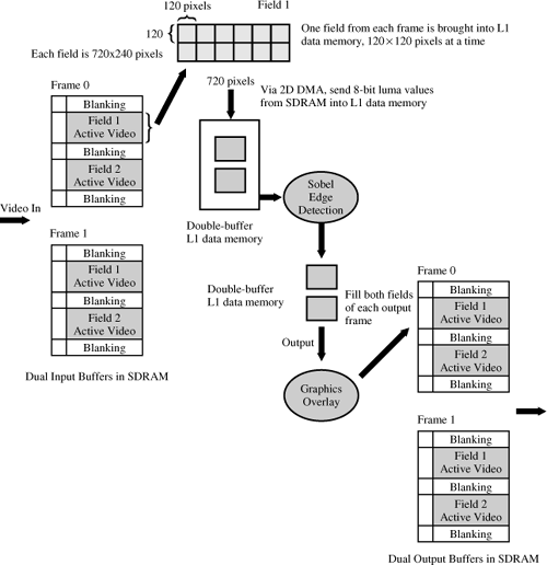
One way to remedy this situation is to repeat some data lines (i.e., bring them into the processor multiple times). This allows you to present the algorithm with “clean” frames to work on, avoiding wraparound artifacts. You should be able to see that the added overhead associated with checking for a wraparound condition is circumvented by instead moving some small amount of data twice. By taking these steps, you can then maintain the programming model you started with by passing a pointer to the smaller subimage, which now resides in internal memory.
The third framework we’ll discuss is often important for algorithms that push the limits of the target processor. Typically, developers will try to right-size their processor to their intended application, so they won’t have to pay a cost premium for an overcapable device. This is usually the case for extremely high-volume, cost-sensitive applications. As such, the “performance-based” framework focuses on attaining best performance at the expense of a possible increase in programming complexity. In this framework, implementation may take longer and integration may be a bit more challenging, but the long-term savings in designing with a less expensive device may justify the extra development time. The reason there’s more time investment early in the development cycle is that every aspect of data flow needs to be carefully planned. When the final data flow is architected, it will be much harder to reuse, because the framework was hand-crafted to solve a specific problem. An example is shown in Figure 7.23.
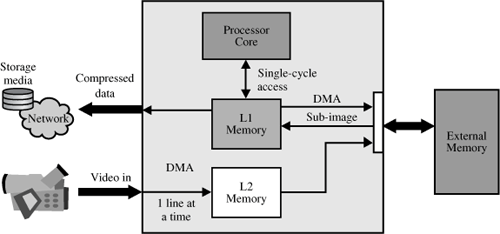
The examples in this category are many and varied. Let’s look at two particular cases: a design where an image pipe and compression engine must coexist, and a high-performance video decoder.
Our first example deals with a digital camera where the processor connects to a CMOS sensor or CCD module that outputs a Bayer RGB pattern. This application often involves a software image pipe that preprocesses the incoming image frame. In this design, we’ll also want to perform JPEG compression or a limited-duration MPEG-4 encode at 30 fps. It’s almost as if we have two separate applications running on the same platform.
This design is well-suited to a dual-core development effort. One core can be dedicated to implementing the image pipe, while the other performs compression. Because the two processors may share some internal and external memory resources, it is important to plan out accesses so that all data movement is choreographed. While each core works on separate tasks, we need to manage memory accesses to ensure that one of the tasks doesn’t hold off any others. The bottom line is that both sides of the application have to complete before the next frame of data enters the system.
Just as in the “Processing on-the-Fly” framework example, lines of video data are brought into L2 memory, where the core directly accesses them for preprocessing as needed, with lower latency than accessing off-chip memory. While the lower core data access time is important, the main purpose of using L2 memory is to buffer up a set of lines in order to make group transfers in the same direction, thus maximizing bus performance to external memory.
A common (but incorrect) assumption made early in many projects is to consider only individual benchmarks when comparing transfers to/from L2 and with transfers to/from L3 memory. The difference in transfer times does not appear to be dramatic when the measurements are taken individually, but the interaction of multiple accesses can make a big difference.
Why is this the case? Because if the video port feeds L3 memory directly, the data bus turns around more times than necessary. Let’s assume we have 8-bit video data packed into 32-bit DMA transfers. As soon as the port collects 4 bytes of sensor input, it will perform a DMA transfer to L3. For most algorithms, a processor makes more reads than writes to data in L3 memory. This, of course, is application-dependent, but in media applications there are usually at least three reads for every write. Since the video port is continuously writing to external memory, turnarounds on the external memory bus happen frequently, and performance suffers as a result.
By the time each line of a video frame passes into L2 memory and back out to external memory, the processor has everything it needs to process the entire frame of data. Very little bandwidth has been wasted by turning the external bus around more than necessary. This scheme is especially important when the image pipe runs in parallel with the video encoder. It ensures the least conflict when the two sides of the application compete for the same resources.
To complete this framework requires a variety of DMA flows. One DMA stream reads data in from external memory, perhaps in the form of video macroblocks. The other flow sends compressed data out—over a network or to a storage device, for instance. In addition, audio streams are part of the overall framework. But, of course, video is the main flow of concern, from both memory traffic and DMA standpoints.
Another sample flow in the “performance-based” framework involves encoding or decoding audio and video at the highest frame rate and image size possible. For example, this may correspond to implementing a decoder (MPEG-4, H.264 or WMV9) that operates on a D-1 video stream on a single-core processor.
Designing for this type of situation conveys an appreciation of the intricacies of a system that is more complex than the ones we have discussed so far. Once the processor receives the encoded bit stream, it parses and separates the header and data payloads from the stream. The overall processing limit for the decoder can be determined by:
(# of cycles/pixel)×(# of pixels/frame) × (# of frames/second) < (Budgeted # of cycles/second) |
At least 10% of the available processing bandwidth must be reserved for steps like audio decode and transport layer processing. For a D-1 video running on a 600 MHz device, we have to process around 10 Mpixels per second. Considering only video processing, this allows ~58 cycles per pixel. However, reserving 10% for audio and transport stream processing, we are left with just over 50 cycles per pixel as our processing budget.
When you consider the number of macroblocks in a D-1 frame, you may ask, “Do I need an interrupt after each of these transfers?” The answer, thankfully, is “No.” As long as you time the transfers and understand when they start and stop, there is no need for an interrupt.
Now let’s look at the data flow of the video decoder shown in Figure 7.24.

Figure 7.25 shows the data movement involved in this example. We use a 2D-to-1D DMA to bring the buffers into L1 memory for processing. Figure 7.26 shows the data flow required to send buffers back out to L3 memory.
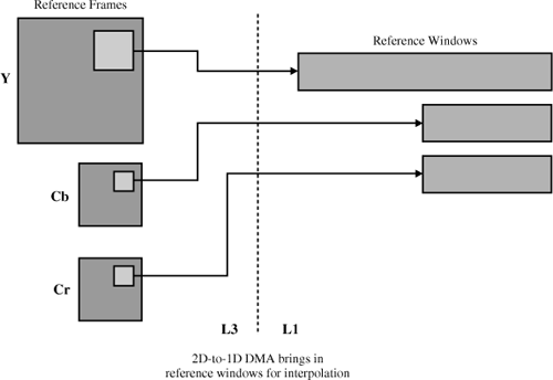

On the DMA side of the framework, we need DMA streams for the incoming encoded bit stream. We also need to account for the reference frame being DMAed into L1 memory, a reconstructed frame sent back out to L3 memory, and the process of converting the frame into 4:2:2 YCbCr format for ITU-R BT.656 output. Finally, another DMA is required to output the decoded video frame through the video port.
For this scheme, larger buffers are staged in L3 memory, while smaller buffers, including lookup tables and building blocks of the larger buffers, reside in L1 memory. When we add up the total bandwidth to move data into and out of the processor, it looks something like the following:
Input data stream: 1 Mbyte/sec
Reference frame in: 15 Mbyte/sec
Loop filter (input and output): 30 Mbyte/sec
Reference data out: 15 Mbyte/sec
Video out: 27 Mbyte/sec
The percentage of bandwidth consumed will depend on the software implementation. One thing, however, is certain, you cannot simply add up each individual transfer rate to arrive at the system bandwidth requirements. This will only give you a rough indication, not tell you whether the system will work.
Aside from what we’ve mentioned above, there are some additional items that you may find useful.
Consider using L2 memory as a video line buffer. Even if it means an extra pass in your system, this approach conserves bandwidth where it is the most valuable, at the external memory interface.
Avoid polling locations in L2 or L3 memory. Polling translates into a tight loop by the core processor that can then lock out other accesses by the DMA controller, if core accesses are assigned higher priority than DMA accesses.
Avoid moving large blocks of memory using core accesses. Consecutive accesses by the core processor can lock out the DMA controller. Use the DMA controller whenever possible to move data between memory spaces.
Profile your code with the processor’s software tools suite, shooting for at least 97% of your code execution to occur in L1 memory. This is best accomplished through a combination of cache and strategic placement of the most critical code in L1 SRAM. It should go without saying, but place your event service routines in L1 memory.
Interrupts are not mandatory for every transfer. If your system is highly deterministic, you may choose to have most transfers finish without an interrupt. This scheme reduces system latency, and it’s the best guarantee that high-bandwidth systems will work. Sometimes, adding a control word to the stream can be useful to indicate the transfer has occurred. For example, the last word of the transfer could be defined to indicate a macroblock number that the processor could then use to set up new DMA transfers.
Taking shortcuts is sometimes okay, especially when these shortcuts are not visually or audibly discernable. For example, as long as the encoded output stream is compliant to a standard, shortcuts that impact the quality only matter if you can detect them. This is especially helpful to consider when the display resolution is the limiting factor or the weak link in a system.
We haven’t talked too much about audio processing in this chapter because it makes up a small subset of the bandwidth in a video-based system. Data rates are measured in kilobytes/sec, versus megabytes/sec for even the lowest-resolution video systems.
Where audio does become important in the context of video processing is when we try to synchronize the audio and video streams in a decoder/encoder system. While we can take shortcuts in image quality in some applications when the display is small, it is hard to take shortcuts on the synchronization task, because an improperly synchronized audio/video output is quite annoying to end users.
For now let’s assume we have already decoded an audio and video stream. Figure 7.27 shows the format of an MPEG-2 transport stream. There are multiple bit stream options for MPEG-2, but we will consider the MPEG-2 transport stream (TS).
The header shown in Figure 7.27 includes a Packet ID code and a sequence number to ensure decode is performed in the proper order. The adaptation field is used for additional control information. One of these control words is the program clock reference, or PCR. This is used as the timing reference for the communication channel.
Video and audio encoders put out packet elementary streams (PES) that are split into the transport packets shown. When a PES packet is split to fit into a set of transport packets, the PES header follows the 4-byte Transport Header. A presentation time stamp is added to the packet. A second time stamp is also added when frames are sent out of order, which is done intentionally for things like anchor video frames. This second time stamp is used to control the order in which data is fed to the decoder.
Let’s take a slight tangent to discuss some data buffer basics, to set the stage for the rest of our discussion. Figure 7.28 shows a generic buffer structure, with high and low watermarks, as well as read and write pointers. The locations of the high and low watermarks are application-dependent, but they should be set appropriately to manage data flow in and out of the buffer. The watermarks determine the hysteresis of the buffer data flow. For example, the high watermark indicates a point in the buffer that triggers some processor action when the buffer is filling up (like draining it down to the low watermark). The low watermark also provides a trigger point that signals a task that some processor action needs to be taken (like transferring enough samples into the buffer to reach the high watermark). The read and write pointers in any specific implementation must be managed with respect to the high and low watermarks to ensure data is not lost or corrupted.
In a video decoder, audio buffers and video frames are created in external memory. As these output buffers are written to L3, a time stamp from the encoded stream is assigned to each buffer and frame. In addition, the processor needs to track its own time base. Then, before each decoded video frame and audio buffer is sent out for display, the processor performs a time check and finds the appropriate data match from each buffer. There are multiple ways to accomplish this task via DMA, but the best way is to have the descriptors already assembled and then, depending on which packet time matches the current processor time, adjust the write pointer to the appropriate descriptor.
Figure 7.29 shows a conceptual illustration of what needs to occur in the processor. As you can probably guess, skipping a video frame or two is usually not catastrophic to the user experience. Depending on the application, even skipping multiple frames may go undetected. On the other hand, not synchronizing audio properly, or skipping audio samples entirely, is much more objectionable to viewers and listeners. The synchronization process of comparing times of encoded packets and matching them with the appropriate buffer is not computationally intensive. The task of parsing the encoded stream takes up the majority of MIPS in this framework, and this number will not vary based on image size.
We have already discussed applications where no operating system is used. We referred to this type of application as a super loop because there is a set order of processing that repeats every iteration. This is most common in the highest-performing systems, as it allows the programmer to retain most of the control over the order of processing. As a result, the block diagram of the data flow is usually pretty simple, but the intensity of the processing (image size, frame rate, or both) is usually greater.
Having said this, even the most demanding application normally requires some type of system services. These allow a system to take advantage of some kernel-like features without actually using an OS or a kernel. In addition to system services, a set of device drivers also works to control the peripherals. Figure 7.30 shows the basic services that are available with the Blackfin VisualDSP++ tool chain.

Of those shown, the external memory and power management services are typically initialization services that configure the device or change operating parameters. On the other hand, the Interrupt, DMA, and Callback Managers all provide ways to manage system flow.
As part of the DMA services, you can move data via a standard API, without having to configure every control register manually. A manager is also provided that accepts DMA work requests. These requests are handled in the order they are received by application software. The DMA Manager simplifies a programming model by abstracting data transfers.
The Interrupt Manager allows the processor to service interrupts quickly. The idea is that the processor leaves the higher-priority interrupt and spawns an interrupt at the lowest priority level. The higher-priority interrupt is serviced, and the lower-priority interrupt is generated via a software instruction. Once this happens, new interrupts are no longer held off.
When the processor returns from the higher-priority interrupt, it can execute a callback function to perform the actual processing. The Callback Manager allows you to respond to an event any way you choose. It passes a pointer to the routine you want to execute when the event occurs. The key is that the basic event is serviced, and the processor runs in a lower-priority task. This is important, because otherwise you run the risk of lingering in a higher-level interrupt, which can then delay response time for other events.
As we mentioned at the beginning of this section, device drivers provide the software layer to various peripherals, such as the video and audio ports. Figure 7.31 shows how the device drivers relate to a typical application. The device driver manages communications between memory and a given peripheral. The device drivers provided with VisualDSP++, for example, can work with or without an operating system.

Finally, an OS can be an integral part of your application. If it is, Figure 7.32 shows how all of these components can be connected together. There are many OS and kernel options available for a processor. Typically, the products span a range of strengths and focus areas, for example, security, performance or code footprint. There is no “silver bullet” when it comes to these parameters. That is, if an OS has more security features, for instance, it may sacrifice on performance and/or kernel size.

In the end, you’ll have to make a trade-off between performance and flexibility. One of the best examples of this trade-off is with uCLinux, an embedded instantiation of Linux that has only partial memory management unit capabilities. Here, the kernel size is measured in megabytes and must run from larger, slower external memory. As such, the instruction cache plays a key role in ensuring best kernel performance. While uCLinux’s performance will never rival that of smaller, more optimized systems, its wealth of open-source projects available, with large user bases, should make you think twice before dismissing it as an option.
In this section we’ve tried to provide guidance on when to choose one framework over another, largely based on data flows, memory requirements, and timing needs. Figure 7.33 shows another slant on these factors. It conveys a general idea of how complexity increases exponentially as data size grows. Moreover, as processing moves from being purely spatial in nature to having a temporal element as well, complexity (and the resulting need for a well-managed media framework) increases even further.
