
If compared to other domains, the embedded development life cycle includes some additional steps. The code must be cross-compiled, the image manipulated then uploaded to a target, tests must be run, and possibly hardware tools are involved in the measurement and verification phases. The life cycle of native, application software, when using compiled languages, looks like this diagram:
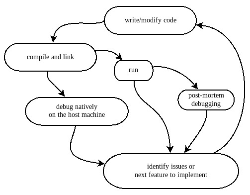
When writing software within the same architecture, tests and debugging can be performed right after compiling, and it is often easier to detect issues. This results in a shorter time for the typical loop. Moreover, if the application crashes because of a bug, the underlying operating system is able to produce a core dump, which can be analyzed using the debugger at a later time, by restoring the content of the virtual memory and the context of the CPU registers right at the moment when the bug shows up. Intercepting fatal errors on an embedded target, on the other hand, might be slightly more challenging because of the potential side effect of memory and registers corruption, in the absence of virtual addresses and memory segmentation, which are provided by the operating systems in other contexts. Even if some targets are able to intercept abnormal situations by triggering diagnostic interrupts, such as the Hard Fault handler in Cortex-M, restoring the original context that generated the error is often impossible.
Furthermore, every time new software is generated, there are a few time-consuming steps to perform, such as the translation of the image to a specific format, and uploading the image to the target itself, which may take anywhere from a few seconds up to a minute, depending on the size of the image and the speed of the interface used to communicate with the target:

In some of the phases of the development, when multiple consecutive iterations may be required to finalize a feature implementation or detect a defect, the timing in between compiling and testing the software has an impact on the efficiency of the whole life cycle. Specific tasks implemented in the software, which involve communication through serial or network interfaces, can only be verified with signal analysis, or by observing the effect on the peripheral or the remote system involved. Analyzing the electrical effects on the embedded system requires some hardware setup and instrument configuration, which add more time to the equation.
Finally, developing a distributed embedded system composed of a number of devices running different software images may result in repeating the preceding iterations for each of these devices. Whenever possible, these steps should be eliminated by using the same image and different set configuration parameters on each device, and by implementing parallel firmware upgrade mechanisms. Protocols such as JTAG support uploading the software image to multiple targets sharing the same bus, significantly cutting down the time required for the firmware upgrades, especially in those distributed systems with a larger numbers of devices involved.
No matter how complex the project is expected to be, it is in general worth spending as much time as needed to optimize the life cycle of the software development at the beginning, in order to increase the efficiency later on. No developer likes to switch the focus away from the actual coding steps for too long, and it might be frustrating to work in a suboptimal environment where stepping through the process requires too much time or human interaction.
In the following section, a cross-compiling GCC toolchain is examined, through the analysis of its components and the steps required to build an embedded application.