
The control unit
We have seen that the activity of the computer is determined by the instructions that are stored in memory as patterns of 0s and 1s. In this chapter, we consider two approaches to the design of the control unit within the G80 microprocessor. The first approach results in a hard-wired controller, while the second results in a micro-programmed controller. We begin by asking what the control unit must do.
13.1 Requirements of the control unit
In order to process a particular instruction the G80 must first fetch the instruction from memory and then execute that instruction. In the fetch phase the operation code at the memory location pointed to by the Program Counter is read and transferred into the Instruction Register, IR. This pattern of bits within the IR determines what the G80 does next, that is, it determines what the G80 activity is during the execute phase. During this phase, the control unit must generate the signals that control the logic circuits within the G80 in such a way as to perform the required instruction. We call these micro-signals. Thus, in order to execute the instruction ld a,(0×4926) the control unit must produce the micro-signals that load the Memory Address Register, MAR, with 0×4926 to address the required memory location, then assert MREQ and RD. After allowing time for the memory to place its data on the Data Bus, the control unit must assert the micro-signal that loads register A with the data currently on the Data Bus. This is followed by the fetch of the next instruction.
The computer contains registers which hold data to be processed, such as registers A and B, and other registers that contain information necessary to control the operation of the computer, such as the Program Counter, PC, and the Instruction Register, IR. The external memory may also be regarded as a collection of registers, some hold data and others hold instructions. All these registers are interconnected so that the contents of one can be transferred to another. Sometimes the data is passed through the Arithmetic and Logic Unit, ALU, in order to modify the data in some way. Essentially, an instruction is executed by transferring the contents of a register, or the output of the ALU, into another register.
13.2 Register transfers
We saw in an earlier chapter how data can be transferred between registers. Referring back to Figure 5.5 (page 74), to transfer the data in register R0 to R2, the required sequence of steps is:
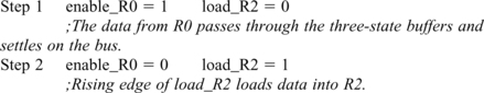
Suppose we want this data transfer to take place when a signal, TP, is asserted. In Figure 13.1, enable_R0 = TP and load_R2 = /TP. When TP is first asserted, enable_R0 is also asserted and load_R2 is de-asserted. The data in R0 appears on the bus after a time, Td, which is the sum of the times for the data to pass through the three-state buffers and for it to settle on the bus. When TP is de-asserted, load_R2 is asserted. The rising edge of load_R2 loads the data from the bus into R2. At the same time, enable_R0 is de-asserted so removing the data from the bus. Thus, the transfer of data is completed. In practice, TP must be asserted for a period that is greater than Td + Tsu,where Tsu is the set-up time of the flip-flops in R2. The set-up time of a flip-flop is the period that the data must be present at the input of the flip-flop before the data is loaded into the flip-flop.
This data transfer may be written concisely as
TP: R2 ← (R0)1
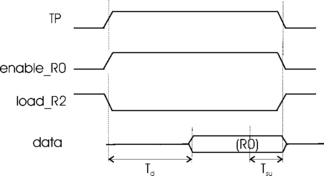
which is read as ‘During the period when TP is asserted, transfer the contents of register R0 to register R2.’ We refer to such statements as micro-operations. These statements are written so that the expression to the right of the arrow evaluates to a data value and the expression to the left evaluates to a register or memory location. Thus ‘R2’ refers to register R2 while ‘(R0)’ refers to the contents of register R2. Similarly, M[adrs] refers to the memory location having address adrs while (M[adrs]) refers to the contents of that memory location. These statements form part of a register transfer language that is useful in describing sequences of micro-operations. The control unit must cause different sequences of micro-operations that fetch and execute the different instructions. These micro-operations are performed at particular cycles of the system clock. Specific clock cycles may be identified by a timing waveform generator circuit, Figure 13.2, which produces a sequence of timing pulses or T-state signals.

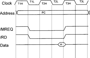
13.3 Instruction fetch
The first byte of an instruction is the operation code, which indicates what the instruction is to do. Thus, the first step is to read the operation code into the Instruction Register, IR, of the G80. This step is called the instruction fetch. The instruction fetch sequence transfers the contents of the memory location that is pointed to by the PC into the IR, that is, IR ← (M[PC]). This may be broken down into the micro-operation sequence:
Operation code Fetch micro-instruction, IR – (M[PC])

This is an example of a memory-read cycle; it generates the external signals shown in the timing diagram, Figure 13.3. The signals MREQ and RD are shown as being asserted when low since this is common practice.
13.4 Examples of instruction execution
Following the op code fetch, the G80 executes the instruction indicated by the pattern of bits in IR. Since the op code fetch occurs during T-states T1 to T3, the execution of an instruction always begins at T-state T4. We consider some typical examples here.
13.4.1 ld d, c
This is a single byte instruction with op code 0×51. It performs the operation D ← (C). It may be executed during T-state T4 as follows:
The second line is read as: ‘When the content of IR is 51 AND T-state T4H is asserted, transfer the contents of register C to register D.’ The total time for the fetch and execution of this instruction is four clock cycles. The final micro-operation resets the Timing Generator so that the next T state will be T1H which begins the next op code Fetch cycle.
13.4.2 Add a, b
This is a single byte instruction with op code 0×80. It performs the operation A ← (B) + (A). It may be performed as follows:
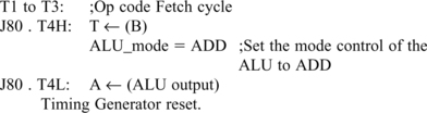
The fetch and execution of this instruction requires four clock cycles.
13.4.3 ld a, n
This is a 2-byte instruction: the number n is stored in the memory location following the op code 0×3E. After the op code fetch sequence, the PC is pointing to this location so the execution of this instruction is simply a memory-read cycle.
The fetch and execution of this instruction requires six clock cycles.
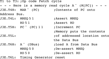
13.4.4 Add a, (hl)
This is a single byte instruction with op code 0×86. It performs the operation A ← (M[HL]) + (A) and thus requires a read of external memory. It may be performed as follows:

The total time for the fetch and execution of this instruction is six clock cycles. Note that during periods T4, T5, and T6, the external signals will appear similar to Figure 13.3 since during these periods the G80 is performing a memory-read cycle.
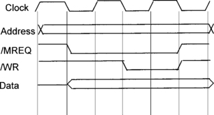
13.4.5 ld (nn), a
This instruction performs the operation M[nn] ← (A). The op code 0×32 is followed in the memory by the two bytes of nn. After transferring the op code into IR, the control unit transfers these bytes into the G80. To provide storage within the G80 for these two bytes, we add two 8-bit registers, called U and V, and also provide that these can be read as a single 16-bit register, UV.

The execution of this instruction comprises two memory read cycles which read the argument nn from the memory, followed by a memory write cycle. The memory write cycle produces the external signals shown in Figure 13.4.
13.4.6 jp nn
This instruction performs the operation PC ← nn. The instruction is 3 bytes long; the first byte is the op code, while the second and third bytes contain the argument nn. The op code 0xC3 is read during the op code fetch cycle. Its execution requires that at the end of the execution phase, the 2 bytes following the op code are to be in the PC. We store these bytes temporarily in register UV, then copy UV to PC.
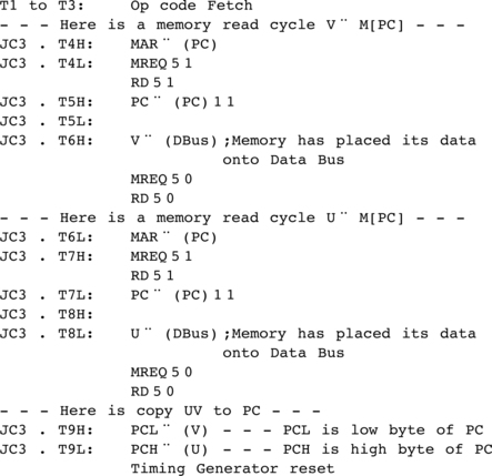
The execution of this instruction comprises two memory read cycles, at the end of which UV contains the argument nn. During T-state T9, the contents of UV are copied to the PC, giving a total of nine clock cycles to fetch and execute this instruction.
13.4.7 jp z, nn
This instruction is similar to the jp nn instruction except that it performs the operation PC ← nn only if the Zero flag is set, otherwise it does nothing. The instruction is 3 bytes long; the first byte is the op code 0xCA, while the second and third bytes contain the argument nn. The argument nn is used only if the Zero flag is set. Thus, some micro-operations are conditional upon the state of the Z flag.

The line z. JCA. t4h: MAR .. (PC) is read as ‘If the Z flag is set AND IR contains 0xCA AND T4H is asserted, copy the content of the PC to the MAR.’
Similarly, /z. JCA. T4H: PC. (PC) 1 1 is read as ‘If the Z flag is not set AND IR contains 0xCA AND T4H is asserted, increment the PC.’
The fetch and execution of this instruction takes nine clock cycles if the Zero flag is set, otherwise it takes five clock cycles.
13.5 Hardwired controller
From the previous section it is seen that each micro-operation is to occur when a logical term such as F. Jxx. Tyy becomes true, where F is the state of a flag, Jxx indicates that the Instruction Register holds xx, and Tyy indicates that the timing pulse generator is asserting T-state Tyy. This leads to the overall structure of the control unit shown in Figure 13.5.

The inputs to the block labelled Combinational Logic are from the decoder, the timing state generator, and the Status flags. Thus, each of the outputs from Combinational Logic depends on these inputs, as required by the micro-operation sequences derived in the previous section. This hard-wired control unit contains a considerable amount of combinational logic.
To determine the logic within the Combinational Logic block of Figure 13.5, a list of all micro-operations is made. Then, a particular micro-operation is chosen. The sequences of micro-operations for all instructions is searched to find the chosen micro-operation and to note the F. Jxx. Tyy condition, which determines when it is to be effected. For example, searching through the examples of micro-operation sequences given in section 13.4, it is seen that the micro-operation U ← (DBus) is required during J32.T8L, JC3.T8L, and Z.JCA.T8L. Thus we can write:
U ← (DBus) = J32.T8L + JC3.T8L + Z.JCA.T8L
From this expression, the combinational logic circuit for the signal to load U from Dbus can be obtained.
Similarly, it is seen that the micro-operation PC ← (PC) + 1 is required during T2H, J3E.T5H, J86.T5H, J32.T5H, J32.T7L, JC3.T5H, JC3.T7L, Z.JCA.T5H, Z.JCA.T7L, /Z.JCA.T4H, and /Z.JCA.T4L. Thus we obtain:
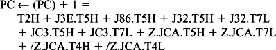
so giving the logic circuit for the signal to increment the PC.
Note that the Boolean expressions given above are derived from the example sequences in section 13.4 only. When the sequences for all the other instructions in the instruction set of G80 are taken into account, the expressions, and hence the logic circuit, becomes large.
13.6 More about the hardwired controller
The logic equations derived in the previous section can become long. The logic may be simplified by assigning the op codes to the instructions in such a way that each bit of the operation code carries information about the type of instruction. This may be done by forming similar instructions into groups. For example, one such group may be formed from instructions of the form ld r,s where r and s represent A, B, C, D, E, H, or L. In the G80, the op codes for these instructions have the binary format 01RRRSSS where:
| Register | RRR, SSS |
| B | 000 |
| C | 001 |
| D | 010 |
| E | 011 |
| H | 100 |
| L | 101 |
| A | 111 |
Thus, ld d,c has op code 01 010 001 or 0×51. When bit 7 of IR = = 0 AND bit 6 of IR = = 1, a transfer between two registers in the register file is indicated. Furthermore, bits 5, 4, 3 indicate the destination register and bits 2, 1, 0 indicate the source register. These bits may be connected directly to encoders that select the registers within the register file.
Similarly, many of the 8-bit arithmetical and logical instructions have op codes of the form 10 PPP RRR where RRR is as given above and PPP is:
| Operation | PPP |
| add | 000 |
| adc | 001 |
| sub | 010 |
| sbc | 011 |
| and | 100 |
| xor | 101 |
| or | 110 |
| cp | 111 |
Thus the op code for xor c is 10 101 001 or 0xA9.
The grouping of instructions allows the equations for the control signals to be written in terms involving just a few bits of IR instead of the fully decoded Jxx signals, so simplifying the logic considerably. However, the logic circuit of a hard-wired control unit is usually large and it can be expected to form a substantial proportion of the microprocessor circuitry.
13.7 Microprogrammed control
The microprogrammed control unit2 is another form of control unit that is widely used in computing machines. We know that the control unit is required to output a different sequence of control signals in order to execute different instructions. The microprogrammed controller stores all these sequences in a ROM. To understand this idea, we begin by looking at how sequences may be generated using a ROM, called the control ROM, or CROM.
13.7.1 Sequence generator
The basic concept is illustrated in Figure 13.6. The CROM contains eight locations, each of which stores 4 bits, that is, it is an 8×4 ROM. The address input to the CROM is taken from a 3-bit counter that is incremented by a clock signal. Thus, each of the locations in the CROM is read out in sequence so generating a sequence of four output signals that are shown as waveforms. The sequence repeats since the counter overflows back to zero.
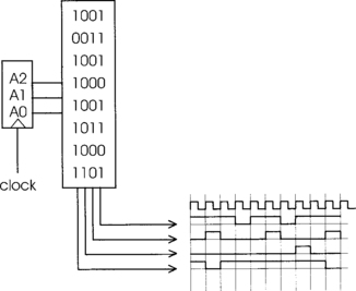
A development of this idea, Figure 13.7, is to replace the counter with a register, the CROM Address Register, and to store the next address within the CROM. The next address, as stored within the CROM, is loaded into the CROM Address Register on every clock pulse. The CROM now contains two fields, the Next Address field and the Control Signal field. Why do this?

The answer is that the CROM can now generate any number of different sequences.
A close examination of the contents of the CROM shown in Figure 13.7 reveals that two different output signal sequences are stored in the CROM. One sequence begins at CROM location 0×00 while the other begins at CROM location 0×05. Thus, if the CROM Address Register, CAR, is initially 0×00, the output sequence will be:
P0, P1, P2, P3, P4, P0, P1, P2, …
Alternatively, if the CAR is initially 0×05, the output sequence will be:
Run program CROMA.exe. The program appearance is shown in Figure 13.8. Click the Step button about a dozen times. Observe that the contents of the Control Signal field at CROM locations 0×00 to 0×04 are output cyclically. Now click on Load New Address in the menu and enter 00101 to load the CROM Address Register with 0×05. Click Step several times and observe that locations 0×05 to 0×07 are output cyclically. Now load the CROM Address Register with 01000 and click Step several times to observe that a sequence does not have to be stored in successive CROM locations.

To use the CROM sequence generator as a control unit in a computer, we need a sequence for every instruction in the instruction set of the computer. In practice this means that a large number of sequences will have to be stored in the CROM3. How is the appropriate sequence to be selected?
13.7.2 Selecting a sequence
The CROM sequence required to execute an instruction such as ld a,(hl) is determined by the operation code stored in the Instruction Register, IR, of the computer. An obvious possibility is to use the contents of the IR as the CROM address at which the control signal sequence for that instruction begins. That is, we load the CAR from the IR. We immediately recognize a problem: two operation codes may differ numerically by one. Thus 0×57 and 0×58 may both be legitimate operation codes in the computer so the sequence to execute the instruction with operation code 0×57 must occupy only one location in the CROM. There is a simple solution: CROM location 0×57 will contain a Next Address that refers to an unused location in the CROM where a sequence of any length may be placed. We will adopt this solution. The question now is how is the instruction fetch phase of the computer operation to be implemented?
For example, we will design our CROM contents so that the instruction fetch sequence occupies CROM locations 0×1E and 0×1F. This sequence of Control Signals is assumed to copy the next operation code from the RAM into the Instruction Register and into the CROM Address Register. At the end of each execution sequence, the Next Address field will be 0×1E so that the sequence to fetch the operation code of the next instruction will begin. This scheme is outlined in Figure 13.9. For simplicity, it is assumed that there are only four operation codes, 0×00 to 0×03.

Run program CROMA.exe and click on Enable Fetch in the menu. This loads the CROM with the data in Figure 13.9 and loads the CROM Address Register with 0×1E. Slowly click the Step button to see the Fetch sequence copy an operation code from RAM and then enter the appropriate Execute sequence. If you wish, you can change the program code in the RAM by clicking on RAM in the menu. (Remember that only 00 to 03 are valid op codes.)
13.7.3 Conditional branching
To accommodate conditional instructions, such as jp c, fred, two sequences must be generated by the control unit. Which one is actually followed must be made to depend on the state of the G80 status flags. One way of providing this facility is to add a Branch Address field and a Flags field to the CROM as shown in Figure 13.10. The Flags field is 3 bits, one for each of the C, S, and Z flags. The multiplexer4 inputs come from the Next Address and Branch Address fields of the CROM. For instructions that do not depend on the state of a flag, the Flag field of the CROM contains three zeros so that Sel is always 0 and the multiplexer selects its input that comes from the Next Address field of the CROM. In these cases, the controller works as previously described.

For an instruction that depends, say, on the Carry flag, the C bit of the Flag’s field is made to be 1. Now, if the Carry flag is set, Sel is 1 and the multiplexer selects the Branch Address field, which is loaded into the CROM Address Register. However, if the Carry flag is not set, Sel is 0 and the multiplexer selects the Next Address field, which is loaded into the CROM Address Register. Thus, the Carry flag can determine which one of the two alternative sequences is generated by the controller. One of these sequences will generate the Control Signals for the case when the Carry flag is not set, while the other sequence generates the Control Signals for the case when the Carry flag is set.
The CROM in the control unit described here has one bit for each Control Signal and may be over a hundred bits wide. Many variations of the basic ideas discussed here are used in practice with the goal of providing a high execution speed within an acceptable area of silicon. Note that the microprogrammed control unit effectively contains a program to generate the control signals. Indeed, each location is said to contain a micro-instruction and the CROM contains a micro-program. The technique is used in the design of some, but not all, modern microprocessors.
13.8 Problems
1. Derive a possible micro-operation sequence for the instruction jp z,nn. How does your sequence relate to the given sequence for jp z,nn?
2. Derive a possible micro-operation sequence for the instruction jp c,nn. How does your sequence relate to the given sequence for jp z,nn?
3. Derive a possible micro-operation sequence for the instruction jp nc,nn. How does your sequence relate to the given sequence for jp c,nn?
4. Derive a possible micro-operation sequence for the instruction push bc.
5. Derive a possible micro-operation sequence for the instruction pop bc.
The following problems require program CromA.exe.
6. Using the default data in the CROM, click Step about a dozen times. Sketch the micro-signal waveforms generated for the first 11 steps.
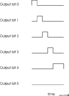
7. Determine the contents of the CROM that produce the sequence of output signals shown in Figure P13.1. Assume the sequence begins at CROM location 00 and that the sequence repeats forever. Use CromA.exe to check your answer.
1Some people prefer to write TP: (R0) → R2.
2The microprogrammed control unit was described by M. V. Wilkes in the early 1950s.
3As noted in the discussion of the hardwired controller, the regularity within the operation codes of a computer helps to reduce the number of sequences required.
4The multiplexer behaves as a two-way switch, connecting one or other of its multi-bit inputs to its output. The position of the switch is determined by the control signal, Sel.