
Specifications of the input and output devices

This device is a bank of eight toggle switches. When the data port SWS is read, this device returns a byte of data each bit of which indicates the state of a switch. The current value of the data port is shown in the ‘Output’ box. A switch toggles when clicked.
![]()
| Data port address: | KEYPAD = 0x80 |
| Control port address: | KEYPAD_C = 0x81 |

When the data port KEYPAD is read, this device returns a byte of data that contains the value of the keypad key that has been ‘pressed’. To press a key, click on it.
The current value of the data port is shown in the ‘Output’ box. The lower 4 bits of the port are the value of the pressed key, 0x0 to 0xF. Bit 7 is the DataReady signal. It is set when a key is pressed and automatically reset when the data port is read. Bits 6, 5, and 4 are unused.
This device may be programmed to generate an interrupt request when a key is pressed by writing 0x83 to the control port, KEYPAD_C. This facility is disabled by writing 0x03 to the control port.
When used with the G80 programmed to have a vectored interrupt response, the interrupt vector is stored in this device by writing the vector, which must be an even number, to the control port.
The current state of the interrupt request may be obtained by reading the control port. Bit 7 is the interrupt flag; when an interrupt request has been made, the control port contains 0x80, otherwise it contains 0x00. Reading the control port automatically resets the interrupt flag.
These properties are summarized in the following table.

| Pad_LCD.asm | Handshaking |
| Int1.asm | Interrupt |
Data port address: PCKBD = 0xC0
This device is the keyboard on the host computer.
When this data port is read a dialog box appears inviting the user to press a key on the keyboard of the host computer. The data returned is the ASCII code for the key.
![]()

This device outputs the position of its slider. The position has a value between 0 and 250. The output position is updated when the slider is released. The slider is moved by dragging it using the mouse cursor with the left button held down. The Page Up and Page Down host computer keys move the slider in steps of 50 while the arrow keys move the slider one step.
![]()
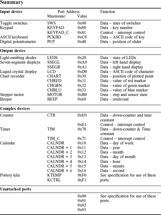
Data port address: LEDS = 0x20
This device is a bank of eight light-emitting diodes. Each LED is connected to the corresponding bit in the data port. If the data bit is 1, the LED becomes red; if the data bit is 0, the LED becomes green.
![]()
![]()
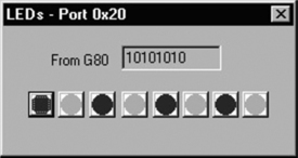
This device comprises two seven-segment displays. A segment is illuminated by writing data that contains a 1 in the bit position corresponding to the segment.

Device: Liquid Crystal Display

The LCD displays the character whose ASCII code is written to the data port. The display has ten lines, each of 20 characters. A line longer than 20 characters automatically wraps to the next line. The display automatically scrolls when more than ten lines are written to it.
A character is written at the current cursor position. The cursor position is automatically moved to the next character position when a character has been displayed.
Some codes, and sequences of codes, control the display as described in the following table.
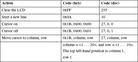
Note: Commercial LCDs usually require a handshake in order to write data to them. This is because they take quite a long time to display a character and so signal when they are ready to receive a new character. For simplicity, the LCD specified here is assumed to be always ready to receive data from the G80.
![]()


This device is a strip chart recorder that plots the input of an 8-bit unsigned integer (0 to 255) on a strip of paper. Every time data is written to port CHART of the device, the data is plotted as an analogue and the drawing position moves on a small step.
Up to three markers may also be plotted. To use a marker, write to one or more of ports CHRED, CHGRN, CHBLU of the recorder before it is used to plot data. The markers plot as red (CHRED), green (CHGRN), and blue (CHBLU) horizontal lines. The default value of all markers is zero. When a marker has a value of zero, it is not plotted.
![]()
Data port address: MOTOR = 0xB0
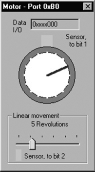
The motor steps through an angle of 22.5° when bit 0 changes from 0 to 1. The direction of the step is controlled by bit 7; when 0 the motor steps clockwise, when 1 the motor steps counter-clockwise. When stepped, the motor must be allowed a short time to move before another step can be initiated.
The data port may be read and written.
When the motor reaches the 12 o’clock position, the sensor connected to bit 1 of the data port is activated.
The motor drives a mechanism such that five complete rotations, 80 steps, of the motor move the traverse from end to end. The traverse wraps from the end to the start. When the traverse is at the start, the sensor connected to bit 2 is activated.
![]()
Data port address: BEEP = 0x60
This device is actually the beeper on the host computer.
A write of any data to this port produces a beep or a click sound.
![]()
Control port address: CTR_C = 0xE1

This device is a model of a factory conveyor belt in which articles are carried by the conveyor belt and pass under a sensor. The output of the sensor is connected to a counter. Each time an article passes under the sensor, the counter is decremented. When the counter reaches zero, it is automatically reloaded with the value shown in the Time Constant box. If the interrupt in the counter circuit has been enabled, an interrupt request is generated to the G80.
To initialize the device, write an 8-bit unsigned integer to port CTR. This number appears in the Time Constant box. (The term ‘time constant’ is used because commercial devices are often ‘timer–counters’; that is, they will count pulse inputs from an external device or count system clock pulses.) When the conveyor belt begins to run, the time constant is copied into the Down counter and the pulses from the object detector decrements this counter. When the Down counter reaches zero, the Zero detect logic reloads the time constant into the Down counter and the process repeats. The contents of the Down counter may be read at any time by reading port CTR.
This device may be programmed to generate an interrupt request when the Down counter reaches zero by writing 0x83 to the control port CTR_C. This facility is disabled by writing 0x03 to the control port.
When used with the G80 programmed to have a vectored interrupt response, the interrupt vector is stored in this device by writing the vector, which must be an even number, to the control port CTR_C.
The current state of the interrupt request flag is obtained by reading the control port. Bit 7 is the interrupt flag; when an interrupt request has been made, the control port contains 0x80, otherwise it contains 0x00. Reading the control port automatically resets the interrupt flag.
These properties are summarized in the following table.

Control port address: TIM_C = 0x71
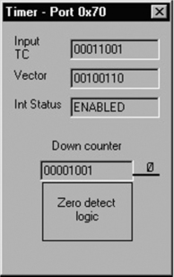
The timer is essentially a hardware counter that is decremented by the system clock. (While this is true for real timers, the simulator decrements the counter in a way that allows you to single step through your programs that use the timer. Because of this the timer is not decremented at equal intervals of time.)
To initialize the device, write an 8-bit unsigned integer to port TIM. This number, the time constant, appears in the Input TC box. When the timer begins to run, the time constant is copied into the Down counter and the system clock (Ø) decrements this counter. When the Down counter reaches zero, the Zero detect logic reloads the time constant into the Down counter and the process repeats. The contents of the Down counter may be read at any time by reading port TIM.
This device may be programmed to generate an interrupt request when the Down counter reaches zero by writing 0x83 to the control port TIM_C. This facility is disabled by writing 0x03 to the control port.
When used with the G80 programmed to have a vectored interrupt response, the interrupt vector is stored in this device by writing the vector, which must be an even number, to the control port.
The current state of the interrupt request flag may be obtained by reading the control port. Bit 7 is the interrupt flag; when an interrupt request has been made, the control port contains 0x80, otherwise it contains 0x00. Reading the control port automatically resets the interrupt flag.
These properties are summarized in the following table.

Data port base address: CLNDR = 0x10
This device is actually the calendar in the host computer.
The calendar is a series of seven counters that keep track of the current date and time. The counters are incremented every second.
Each counter is connected to an 8-bit port. The ports are read only.
| Port address | Value |
| CLNDR+0 | Day of week, 1 … 7. Sunday = 1 |
| CLNDR+1 | Year – 2000: 00..99 |
| CLNDR+2 | Month, 1 … 12. January = 1 |
| CLNDR+3 | Day of month, 1 … 31 |
| CLNDR+4 | Hour, 00 … 23 |
| CLNDR+5 | Minute, 00 … 59 |
| CLNDR+6 | Second, 00 … 59 |
![]()
Data port address: KTEMP = 0xF0
Control port address: KCTRL = 0xF1

This device is a model of a pottery kiln. The kiln heater is switched on or off by bit 0 of port KCTRL. A temperature sensor is connected to an amplifier and an 8-bit analogue-to-digital converter (ADC). The output of the ADC is connected to port KTEMP. The ADC is configured to automatically convert the temperature to a digital value at regular intervals of time. On completing a conversion, the ADC sets bit 7 of port KCTRL, so indicating that a new temperature value is available. When the temperature is read from port 0xF0, bit 7 of port KCTRL is automatically reset.
The value of the least significant bit of the ADC output is 5°C. Thus, when the ADC output is 60, the kiln temperature is 300°C. The kiln temperature ranges from 20°C, the ambient temperature, to 1250°C, the maximum temperature.
The model of the kiln dynamic behaviour is that of a first order system. The heating time constant used in the model defaults to ‘long’ but may be set to ‘short’ to reduce the time required to test a program that controls the kiln. The cooling time constant is five times the heating time constant.
![]()
Device: Ports with no attached devices and with no interrupt logic
Data port addresses: 0x00, 0x01, 0x02, 0x03
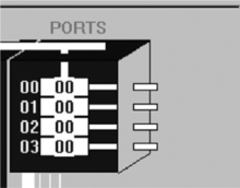
These four data ports may be read or written. The ports contain no logic for generating an interrupt request.
The port data is shown in the appropriate port data register. The contents of this data register may be changed by double-clicking in the ports region of the simulator display when in the single-step mode.
![]()
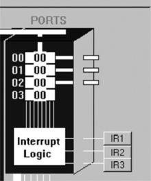
Device: Ports with no attached devices and with interrupt logic for mode 0
Data port addresses: 0x00, 0x01, 0x02

Ports 0x00, 0x01, and 0x02 may be read or written. However, port 0x03 is used as the control port for the interrupt logic.
When any of the interrupt request buttons, IR1, IR2, or IR3, is asserted by clicking on it, the port logic circuit asserts the interrupt request signal, INT, to the G80. At the same time, the port logic circuit loads port 0x03 with the code for one of the restart instructions. If IR1 is asserted, the logic in the port loads port 0x03 with the code for the rst 10 instruction. Thus, the interrupt service routine for IR1 must start at memory location 0x0010. Similarly, the interrupt service routine for IR2 must begin at location 0x0020, and that for IR3 at 0x0030.
The port data is shown in the appropriate port data register. The contents of this data register may be changed by double-clicking in the ports region of the simulator display when in the single-step mode.
![]()
Device: Ports with no attached devices and with interrupt logic for mode 1
Data port addresses: 0x00, 0x01, 0x02
Ports 0x00, 0x01, and 0x02 may be read or written. However, port 0x03 is used as the control port for the interrupt logic.
When any of the interrupt request buttons, IR1, IR2, or IR3, is asserted by clicking on it, the port logic asserts interrupt request signal, INT, to the G80. At the same time, the port logic sets the lower bits of port 0x03 according to which of the IRx buttons was asserted. IR1 causes bit 0 to be set, IR2 causes bit 1 to be set, and IR3 causes bit 2 to be set. Thus, the interrupt service routine must read port 0x03 in order to determine which of the IRx inputs caused the interrupt request.
The port data is shown in the appropriate port data register. The contents of this data register may be changed by double-clicking in the ports region of the simulator display when in the single-step mode.
![]()
Device: Ports with no attached devices and with interrupt logic for mode 2
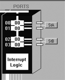
Ports 0x00 and 0x02 may be read or written. However, port 0x01 holds the interrupt vector for port 0x00, and port 0x03 holds the interrupt vector for port 0x01.
When either of the interrupt request buttons, StA or StB, is asserted by clicking on it, the port logic asserts the interrupt request signal, INT, to the G80.
The port data is shown in the appropriate port data register. The contents of this data register may be changed by double-clicking in the ports region of the simulator display when in the single-step mode.
![]()