The best way to reduce bugs in a design is to minimize the opportunities that bugs can be introduced—in other words, design with verification in mind. Once this objective is achieved, the next step is to maximize the simulation speed of the design. These two objectives can be accomplished right from the beginning with the cooperation of Hardware Descriptive Language (HDL) designers by introducing coding style rules to which designers must adhere. These rules restrict the kinds of constructs a designer can write and make the code more regular in structure and easy to understand. As an example, consider the following code:
wire [8:0] in;
wire [7:0] out;
assign out = in;
This segment of code is perfectly legal. Because signal out is 1 bit shorter than in, the most significant bit (MSB) of in will be truncated, which may be the designer’s intent. However, it is also very likely that an error was introduced in the declaration of signal in, when the designer meant [7:0] for the 8-bit signal. To eliminate the ambiguity in this assignment, a rule can be established to force designers to make their intent explicit by requiring that the right-side variable and the left-side variable have equal width.
One may argue that coding guidelines diminish the expressiveness of the language and thus may create inefficient code. In practice, the benefits of minimizing bug-introducing opportunities far outweigh the potential lost code efficiency.
There are generally several coding guideline categories, each emphasizing a particular domain. Typical categories include
Functional correctness
Timing correctness
Simulation performance
Portability and maintainability
“Synthesizability,” “debugability,” and general tool compatibility
In addition, there are other special applications that require their own coding guidelines:
Cycle-based simulation
Hardware simulation/emulation
Two-state simulation
Functional correctness rules attempt to eliminate the hidden side effects of some constructs by requiring the designer to state explicitly the coding intent. Requiring a matching width for all operands is an example of a coding guideline for functional correctness. Rules for timing correctness examine code that may cause race problems, glitches in clock trees, and other timing problems. Portability and maintainability rules enforce project code partition and structure, naming convention, comments, file organization, and so on. Rules for simulation performance flag slow code and recommend styles that yield faster simulation. Finally, rules for tool compatibility ensure the code is acceptable by other tools used in the project (for example, synthesizability for synthesis tools). The three special categories listed earlier apply to particular simulators.
Checking for coding guidelines is static—namely, no input vectors are required and violations can be determined by examining the code alone, even for the timing correctness category. The tool used to enforce coding guidelines is usually called a linter. Traditionally, a linter is used to check syntactical errors and warnings (for example, left and right operands have mismatched lengths). As people realized that many design errors can be checked statically, the role of the linter has expanded beyond simple syntactical checks. Examples of expanded linting are combinational loops, and timing problems on a clock tree. For simplicity’s sake I refer to a linter as a tool that checks for all the errors and warnings discussed in this chapter, although I must point out that the term linter has become slightly abused.
Errors and warnings in coding guidelines form a spectrum of difficulty. Some design constructs may be inferred with certainty as errors, whereas others may be variants that deviate from a predetermined guideline. The former is one extreme of the spectrum and the latter is the other extreme. In between are errors and warnings with varying degrees of severity. Therefore, a linter usually issues levels of severity along with errors and warnings.
Some constructs in a design can be analyzed just by examining the code locally without knowing how it is connected to the rest of the circuit, whereas others require a more global scope. For example, the assignment in the sample in the previous section reveals a potential error. But an error of a loop consisting of combinational gates cannot be detected just by looking at a gate in the loop; the error can only be discovered by examining how the gates are connected (in other words, the structure of the circuits must be checked). Therefore, we classify checks into two categories: syntactical and structural. The first category can be analyzed locally and the second must be done globally.
Because design codes are examined not just for errors but also for potential errors or undesirable coding styles, which may vary from project to project, instead of having a set of fixed rules, each project has its own set of design guidelines. It is not possible nor is it fruitful to enumerate all possible rules. Instead, let’s study some common rules that all projects should enforce.
All operands of an operator must be of equal width. Although most language such as Verilog automatically pad the shorter operands with zeros to make them of equal length, it’s a good practice to have the designer make this explicit to avoid careless mistakes. An example of equal and unequal operand widths is shown here. Two operators are presented. The first one is a bitwise AND and the second is the assignment. The first assign is correct because the operands X, Y, and Z are all declared to be 32 bits wide. The second assign is also correct, because the operands X[10:2], Y[8:0], and Z[11:3] are all 9 bits wide, where X[10:2] means the part of bus X from bit 2 to bit 10. The third assign violates our equal-width guideline, because Z is 32 bits wide but the two operands on the right side are 9 bits and 8 bits wide respectively. Finally, in the last assignment, zeros are padded to an operand to make the operands equal width, where {} is a concatenation operator that combines the 1-bit constant 1’b0 with the 8-bit signal Y[8:1] to form a 9-bit signal:
reg [31:0] X;
reg [31:0] Y;
reg [31:0] Z;

Z = X & Y; //all operands have equal width
Z[11:3] = X[10:2] & Y[8:0]; // all operands have equal width
Z = X[9:1] & Y[8:1]; // error: unequal operand width
Z[8:0] = X[9:1] & {1'b0,Y[8:1]}; // pad with zeros for equal width
While operands should have equal width, the width of the variable holding the operation result must be able to accommodate the result. In a 64-bit adder, the width of the sum is 65 bits, with the MSB holding carry-out. Similarly, in a 64-bit multiplier, the width of the product is 128 bits.
Implicitly embedded sequential states result from a specification that has memory but does not explicitly create states. One such case is incompletely specified conditional statements. Conditional statements such as if-then-else and case statements need to have all cases specified. Failure to do so may result in unexpected circuit behavior. Consider the following description:
case(X) // a 2-bit variable
2'b00: Q = 1'b1;
2'b11: Q = 1'b0;
endcase
In this case statement, the value of the 2-bit variable X is compared first with value 2’b00 (a 2-bit value of 00). If it matches, variable Q is assigned a value of 1. Next, X is compared with value 2’b11. If it matches, Q takes on value 0. Here, only two of four possible values are specified. Thus, if X takes on value 01 or 10, Q retains the old value—that is, this code segment has memory. Thus the code, although it has the appearance of a multiplexor, is of a sequential nature because of the missing two cases (01 and 10). This implied sequential behavior should be made explicit if it is intended to be so; otherwise, the implied sequential behavior should be removed by completing the cases, as shown here:
case(X) // a 2-bit variable
2'b00: Q = 1'b1;
2'b11: Q = 1'b0;
default: Q = 1'b0;
endcase
Similar situations apply to if-then-else statements. This implied sequential behavior is also known as the inferred latch phenomenon, because a latch or sequential element will be needed to preserve the value of Q in the absence of the default statement. To make this inferred latch phenomenon more concrete, let us construct a circuit implementing the previous description. An implementation is shown in Figure 2.1, where the flip-flop (FF) is required to preserve the state. Here we assume the case statement resides inside an always block with clock clk.
To avoid inferred latches, one can either fully specify all possible values of the conditioning variable or use a directive to instruct the synthesis tool not to generate inferred latches and to treat the unspecified values as don’t-cares. This directive is a special comment that the synthesis tool understands and is often termed full_case, meaning that the case statement should be treated as if it were fully specified; if the conditioning variable takes on the unspecified cases, the output variable can take on any value (in other words, don’t-cares for the synthesis tool). Note that because this directive appears as a comment, it has no effect on the simulator. If a full-case directive were used in Figure 2.1, then it would mean that when X is either 01 or 10, Q can be any value. In other words, with these unspecified cases taking on don’t-care values implicitly, the conditional statement is now fully specified—it has all (full) cases. When a synthesis tool sees a full_case directive, it can assign any value to the unspecified cases, as opposed to retaining the current value, and thus no latches are required to retain the current value. When a don’t-care is encountered, a synthesis tool uses it for optimization (for example, producing a smaller circuit). The following example illustrates the use of don’t-cares in synthesis.
Consider the following code segment and two versions of its implementation, one using the unspecified cases for the purpose of minimizing gate count and the other not:
always @(posedge clock) begin
   case (S):
      3'b000: Q = a;
      3'b011: Q = b;
      3'b101: Q = a;
      3'b111: Q = b;
   endcase

assign F = ( (S == 3'b100) | (S == 3'b001) ) ? (a | b) : Q;
An implementation is shown in Figure 2.2, where the FF and the multiplexor implement the incomplete case statement and other gates, the assign statement.

When we place a full_case directive next to the case statement:
case (S): // synthesis full case
Then the synthesis tool recognizes the don’t-care values of Q in the unspecified cases and uses them to optimize gate count. One optimization technique is to choose Q to be (a | b) when S is either 001 or 100. So, Q’ and F’, the resulting Q and F, become
case (S): // synthesis full case
   3'b000: Q' = a;
   3'b011: Q' = b;
   3'b101: Q' = a;
   3'b111: Q' = b;
   3'b001: Q' = a | b;
   3'b100: Q' = a | b;
   3'b010: 0;
   3'b110: 0;
endcase
Note that Q’ can be written as (S==3’b100)|(S==3’b001))?(a|b):Q, which is just F. Therefore, assign
F = Q';
With this choice of don’t-care, the new description yields the much simpler circuit shown in Figure 2.3.

Although using a full_case directive has the advantage of giving a synthesis tool more freedom for optimization, it has the side effect of creating two different versions from the same design description. One is the simulation version, for which the simulator assigns the current value to the output if the unspecified case is encountered. The second is the synthesized circuit, for which the output takes on whatever value the synthesis tool deems optimal. The danger of having a simulation version that is different from the synthesis version is obvious: You are not verifying what you are designing.
Another common source of creating an implied sequential state is a variable read in a block that is not on the block’s sensitivity list, and none of the variables on the sensitivity list is a clock. (If one variable on the sensitivity list is a clock, the block models a latch, and is less likely a user error.) This type of description can result from a user who wants to model a combinational block but inadvertently leaves out a variable on the sensitivity list. To see why an incomplete sensitivity list gives rises to a sequential circuit, consider the following code. A change in X does not cause variable Y to be updated until there is a transition on Z. Meaning, before the transition of Z, Y still holds the old value of X; therefore, the block exhibits memory and thus is sequential:
always @(Z)
Y = X & Z;
A warning needs to be issued if such a situation occurs. However, if a warning is issued for every such occurrence, there would be many warnings for intended FFs and other sequential elements. To avoid flooding of warnings, intended sequential elements should always be instantiated from library cells for which such check should be skipped.
Another anomaly of case statements results from the order the condition variable compares against the case items. In the following case statement, condition variable S compares its value against the case items from top to bottom—namely, first 1?? and then ??1, where ? is a wild card that matches either 1 or 0. When a match is found, the corresponding statement is executed and the remaining case items are skipped. Therefore, when S is 101, S matches 1??, and therefore Q is assigned 0 even though 101 also matches the second case item ??1:
Casex (S)
   3'b1??: Q = 1'b0;
   3'b??1: Q = 1'b1;
endcase
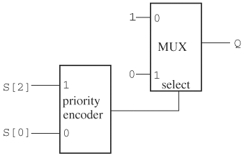
This first matched/first assigned nature implies a priority encoder in the case statement (in other words, the earlier case items have higher priorities). An N-bit encoder takes in 2N bits, of which only 1 bit is active (for example, 1), and it produces a binary code for the bit (for example, 101 is the output if the fifth bit is 1). A priority encoder can accept more than one active bit, but it only produces the code for the active bit with the highest priority.
If this case statement is given to a synthesis tool, a priority encoder will be produced. A portion of the circuit is shown in Figure 2.4. (This case statement is incomplete; therefore, a sequential element is needed to model completely the specification. For clarity, we only show the portion involving the priority encoder.) As dictated by the description, if the MSB of S, S [2], is 1, Q is assigned 0 regardless of the value of its least significant bit (LSB). In this case, the priority encoder gives 1, which selects 0 in the multiplexor. Having a priority encoder for a case statement may not be what the designer had in mind. If S[0] is 1 and S[2] is 0, then the priority encoder gives 0, which makes the multiplexor produce a 1. Note that if we can guarantee that only one case item will match the case variable, then a simple encoder can be used.
Therefore, if the designer is certain that variable S can never have a value straddling the two ranges of the case items, then she can instruct a synthesis tool not to use a priority encoder. Having only one match also means that comparisons with case items can be done in parallel. To relay this information to a synthesis tool, the designer can place a parallel-case directive (for example, //synthesis parallel case) next to the case statement.
Although the parallel-case directive rescues designers from having an implied priority encoder, there are side effects. First, the directive affects only synthesis tools, not simulators. Thus, two models exist: A simulator sees a prioritized case statement and a synthesis tool interprets a parallel case statement. Again, the model being verified is not what is being designed—a dangerous double standard. What would happen if a parallel-case pragma is specified anyway, even though the case items overlap? The synthesized circuit may vary from one synthesis tool to another. An intelligent synthesis tool will use a priority encoder to resolve the conflict; others may just follow the pragma to use an encoder. Therefore, to ensure that the synthesis model and simulation model are consistent, case items should always be mutually exclusive.
There are ways to connect and access components, but explicit ones are preferred, thus reducing the chances of inadvertent mistakes. In Verilog there are two ways to connect ports during module instantiation. The implicit way connects instantiated ports with declared ports in a one-to-one correspondence in order. For example, in Figure 2.5, module Gate declares ports in order Q1, Q2, and Q3, and instance M1 declares ports in order P1, P2, and P3. Thus, connection by order connects P1 with Q1, P2 with Q2, and P3 with Q3.
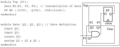
Explicit connection connects instantiated ports and declared ports by name. Continuing the previous example, instance M2 has the same port connection as M1, even though its port order is different:
Gate M2 (.Q2(P2), .Q3(P3), .Q1(P1)); // explicit port connection
Instance FF in Figure 2.5 uses explicit connection, and the block diagram shows the actual connections. Explicit connection is less error prone and is preferred over connection by order.
Furthermore, no expression is allowed during port connection. For example, instead of having
Gate M2 (.Q2(P2&R), .Q3(P3), .Q1(P1));
where input port Q2 is fed with express P2&R. One should create a variable that computes the expression and then gets connected to port Q2, as in
assign V = P2 & R;
Gate M2 (.Q2(V), .Q3(P3), .Q1(P1));
The rationale is to separate logic computation and port connection for a better structured design.
Besides going through a port, the so-called hierarchical path is another way to access a signal. In a design there are usually several levels of hierarchies (or levels of module instantiation). For example, in a central processing unit (CPU) design, the top module is a CPU that contains several modules, such as a floating point unit (FPU), and a memory management unit (MMU). In turn, the FPU may contain several modules, such as an Arithmetic Logic Unit (ALU) and others. One can access net N inside the ALU from anywhere in the design through a hierarchical path, without going through the sequence of ports from the CPU to the FPU to the ALU. To write the value of N to another net M, one simply uses
assign M = CPU.FPU.ALU.N; // access by hierarchical path
In a project, two types of HDL code exist. One type belongs to the design (the code that constitutes the chip) and the other belongs to the test bench (the code that forms the testing structure). It’s strongly recommended that hierarchical accesses exist only in the test bench. In other words, the design should contain no hierarchical paths. The rationale is that access in hardware is always through ports; therefore, the design description should reflect this to be consistent. However, a test bench is used only for testing purpose. No real hardware will be fabricated from it. Therefore, it is reasonable to use hierarchical access.
Finally, it’s a good practice to require that the top-level module have only module instantiations. That is, no logic circuitry. The reason for this is that having logic at the top level is indicative of poor design partitioning—namely, the logic not properly assigned to any submodules. Furthermore, the partition of modules at the RTL should correspond to the physical partition. This simplifies the equivalence checks between the RTL and the physical design.
Some legal constructs are discouraged for several good reasons. Because it is not possible to enumerate all of them (some are project specific), let’s take a look at the common ones. Loop constructs such as FOR/WHILE/REPEAT are discouraged for design code (test bench code has more relaxed rules). The reason for this is that the loop structure is more of a software entity than a hardware entity. Using them in the RTL creates a less direct correspondence between the RTL and the real hardware, making verification more complex. Sometimes loop constructs are used to create regular structures. An example is a memory array, which consists of a large, repetitive regular structure. A macro should be used instead, because directly coding a large, repetitive structure is error prone, whereas automatic macro generation gives the user an easy way to inspect for correctness. Macros can be written in Perl, m4, or C and, when called during preprocessing, will write out a Verilog description of the code.
When coding at the RTL, lower level constructs such as gate and transistor primitives should be avoided, some of which are AND, NOR, NOT, PMOS, NMOS, CMOS, TRAN, TRIREG, PULLUP, and PULLDOWN. The first three are logic gates, the next five are transistors, and the last two are resistive PULLUPs and PULLDOWNs. Furthermore, Verilog has a syntax for signal strength that is used to resolve conflict when a net is driven to opposite values at the same time. The signal with the greater strength wins. Strength constructs belong to transistor-level design and should be avoided in RTL code.
In addition, some constructs are mainly for test benches, for which no hardware counterpart is produced and thus have a coding style that can be more software oriented than hardware oriented. Examples of such Verilog constructs are force/release, fork/join, event, and wait.
Finally, user-defined primitives (UDPs), especially sequential ones, should be avoided as much as possible, because their functionality is not immediately obvious and they often hide unexpected side effects. The workaround is to replace UDPs with small circuits made of standard library cells.
Structural errors and warnings result from connections between components. To detect them, code from multiple designers may be required for examination, and they may be much less obvious to individual designers.
A loop structure is a loop made of circuit components with outputs that feed to the inputs of the next component in the loop. An example is shown in Figure 2.6. A loop structure is detrimental if, at a moment in time, the signal can travel along the loop uninhibited—that is, not blocked by an FF or a latch. A case in point is a loop made of only combinational gates. Another situation is a loop made of latches that can all become transparent at the same time. The latch loop in Figure 2.6 can become transparent if clock1 is high and clock2 is low.

A combinational loop can be detected by following combinational gates from input to output. When you arrive at the same net without going through a sequential device, you have found such a loop. A latch loop is more difficult to discover because, besides finding a loop of latches and combinational gates, you need to determine whether all latches in the loop can become transparent at the same time, and this decision is computationally expensive. In practice, the designer assists the checker by telling her about the phases of latch clocks. Even with hints, the checker may still make pessimistic assumptions and may have the designer validate or invalidate the latch loops.
A bus is a communication channel among devices that have the capability to relinquish the bus by driving its outputs to high impedance Z. Thus, all gates connected to a bus must be tristate devices. In theory, a bus should be in high impedance state when it is not driven. In practice, some designs pull up (or down) a floating bus with a weak resistor to avoid being a potentially problematic dangling net. The strength of the pull-up or pull-down resistor should be chosen to be just right to not have the bus stuck at one logic level. Given this complication, warnings should be issued in this situation.
Furthermore, drivers to a bus should be checked for mutual exclusion of their enable signals (in other words, at most, one driver of the bus can be active) at any time. A conclusive check is computationally expensive and belongs to the domain of formal verification. A compromise is to check mutual exclusion during simulation runs. Then, of course, the result is data dependent and indicates only partial validation. It is also desirable to ensure that when a bus receiver is enabled, a driver is already driving, or when a driver is active, at least one receiver is listening. Again, these checks should be done with formal verification tools or during simulation runs.
Sequential elements are latches and FFs. How they are connected requires particular attention. Active high latches should not drive active high latches, and positive-edge trigger FFs should not drive active high latches, because the driven latches simply pass whatever the driving latches/FFs store, behaving just like buffers. This kind of configuration should invoke warnings, but not errors, because the driven latches could probably be used for other purposes than storage, such as for scanning. Similarly, an active low latch should not be driven by another active low latch or negative-edge trigger FF. Therefore, phases of sequential elements should alternate along any path.
Checking for sequential element configuration becomes complicated when there are multiple clock domains—namely, parts of the design are driven by different clocks. Then the simple phase-alternating rule would generalize to check whether a driven sequential element retains its storage functionality. Again, it is not possible to be conclusive about whether a violation is necessarily an error; hence, a warning should be issued.
All sequential elements in control logic should be able to be reset or be able to be driven to a known state. The reason is that when the design is first powered on, the control logic should be in a known state. However, such a requirement is not necessary for the sequential elements in data path logic, which, if designed properly, is supposedly drivable to a known state.
Contrary to common belief, timing correctness, to certain degree, can be verified statically in the RTL without physical design parameters such as gate and interconnect delays. In this section, we discuss some timing problems that can be discovered at RTL.
The foremost common timing problem is race. A race problem can be defined as the process that results in nondeterministic outcome when several operations operate on the same entity (such as variables or nets) at the same time. Therefore, the resulting outcome is at the mercy of the simulator or the physical devices. The operations can be simultaneous multiple writes or simultaneous read and write. Race problems manifest as intermittent errors and are extremely hard to trace from the design’s input/output (I/O) behavior.
Race problems have many causes. The following race problems are common in practice and can be easily detected from the HDL description. The first type is assignment to the same variable from several blocks triggered by the same clock edge or event. The following circuit shows a Verilog example of a race problem caused by the write operations (in other words, assignment) from two always blocks triggering on the same clock edge, for which the value of x is simulator dependent.
always @(posedge clock)
   x = 1'b1;

always @(posedge clock)
   x = 1'b0;
A less obvious multiple write is the so-called event-counting construct shown next. Each transition of x or y causes a write to variable event_number. The problem arises when x and y have transitions at the same time. In this case, whether event_number is incremented by two or one is simulator dependent and thus nondeterministic:
always @(x or y)
event_number = event_number + 1;
An example of a simultaneous read and write is shown next, where a change in the value of y (caused by y = y + 1) triggers the continuous assignment (assign x = y + 2), which in turn writes a new value to x. At the same time, x is assigned z. The problem lies in what value z would get—the x value before the continuous assignment update or after? The resulting z is nondeterministic:
assign x = y + 2;
always (posedge clock) begin
   y = y +1;
   z = x;
end
In summary, when a variable is multiply written or written and read at the same time, race problems exist.
HDL beginners often commit a common read and write race mistake in using blocking assigns in FFs, as shown in the following example:
module FF (D, clock, Q) ;
   input D;
   input clock;
   output Q;
   always @(posedge clock)
      Q = D;
endmodule

module two_FFs;
   FF m1(.D(Q2),.Q(Q1),.clock (clock);
   FF m2(.D(Q1),.Q(Q2),.clock (clock);
endmodule
When two such FFs are connected in series, as in module two_FFs, net Q1 is read by the second FF and is written by the first FF at the same time. What the second FF sees is uncertain and varies from simulator to simulator. The remedy is to change the blocking assigns to nonblocking assigns. A nonblocking assign reads the value and holds off writing until the end of the current simulation time, at which time all reads are already finished.
In general, to eliminate read/write race problems, nonblocking assigns should be used in place of blocking assigns, because nonblocking assigns read the values when the statement is reached, and write at the end of the current simulation time, at which time all reads have been finished. As a result, no read and write can happen at the same time. However, using nonblocking assigns does not get rid of write/write race problems: All writes still occur simultaneously at the end of the current simulation time.
Glitches are unintended pulses resulting from design artifacts and have widths that vary according to physical parameters (such as parasitic capacitance and trace length) and operating conditions (such as temperature and the chip’s state). As these conditions change, glitches vary their widths, and consequently may get filtered out or may cause errors at random. Hence, glitches are a major source of intermittent error. Let’s study several common causes of glitches.
Clock gating is a common design practice and, if not used properly, can produce glitches on the clock tree to trigger latches and FFs falsely. Let us start with the example in Figure 2.7, in which the gating signal is the output of the FF clocked by the same clock. Assume the gating signal changes from high to low at the rising edge of the clock. Because of the delay from clock to Q in the gating FF, the gating signal arrives slightly later than the clock rising transition and thus causes a narrow glitch.
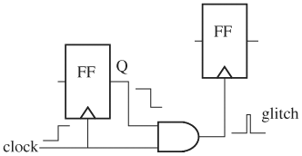
One may propose to add a delay to the clock line to ensure clock rising transitions arrive late, to get rid of the glitch. There are two problems with this solution. First, factors affecting the relative delays are abundant and hard to control. For example, layout lengths and the actual gate delays depend on layout tools and fabrication processes. Second, zero-delay simulation (all gates are treated with zero delay), often employed for the RTL, still produces the glitch, because a simulator always delays the output of an FF by an infinitesimal amount relative to the clock, because of a nonblocking assign for the output of the FF, regardless of the actual delays.
A clean solution is to use an OR gate as the gating device. In this setup, the clock transits to high first to stabilize the output of the OR gate, hence preventing glitches. Similarly, if the gating FF is negative-edge triggered, the gating device should be an AND gate. In summary, if the gating signal changes on the clock’s rising edge, an OR gate should be the gating device. Conversely, if the gating signal changes on the falling edge, an AND gate should be the gating device.
Simple gates such as AND and OR should be used as gating devices because complex ones often produce glitches for certain combinations of input transitions. In addition, gating devices should be instantiated from library cells, instead of created at will as part of the RTL design, so that these timing-critical gates can be under strict control throughout the entire project.
Taking this one step further, there is a restriction on the type of latches that can be clocked by a gated clock. Based on the previous clock gating rule, a rising transition signal should be gated by an OR, then the latch receiving the gated clock should be an active low latch because the latch will correctly become opaque when the gating signal turns high to disable the clock. Similarly, for a falling gating signal, i.e., AND gating, the receiving latch should be an active high latch.
Time zero glitches refer to the transitions at the start of the simulation—at time zero. When a clock is assigned to 1 at time zero, should the transition from an unknown value, x, to 1 be counted as a transition or not? The answer depends on the simulator. A solution is to delay assignments to the clock to avoid transitions at time zero.
Closely related to the time zero glitch in name, but not in nature, is the zero time glitch. This type of glitch has zero width and is often an RTL coding artifact for which two different values are assigned to the same variable in no time. This often happens in zero-delay simulation. The following code is indicative of a finite-state machine in which, by initializing next_state to RESET, the designer wanted to make sure that next_state does not end up in an unknown state if current_state is neither ACK nor IDEL. However, if current_state is ACK (IDEL), variable next_state changes from RESET to IDLE (REQ) in no time, creating a zero time glitch in next_state and in glitch_line:
always @(posedge clock) begin
   next_state = RESET; // initialize next_state to RESET
   case (current_state)
      ACK: next_state = IDLE;
      IDEL: next_state = REQ;
end

assign glitch_line = next_state; // executed every time
next_state changes
To eliminate zero time glitches, avoid multiple writes to the same variable in one clock cycle.
Glitches can easily form at interfaces of different clock domains. A clock domain is the group of logic that is clocked by the same clock. Interface logic of two clock domains is the logic with inputs that come from two clock domains—for example an AND gate with one input from one clock domain and another from another clock domain. If the two clock domains are not synchronized, the intervals between the transitions in the two domains can be arbitrarily small as the transitions beat against each other and hence create glitches in the interface logic. Therefore, when clock domains merge, proper synchronization should be in place. A circuit synchronizing two clock domains is shown in Figure 2.8.

It’s almost universally true that the higher level of abstraction of the system, the faster it will simulate. The creation of a system goes through multiple modeling levels, from specification all the way down to the transistor level. A model of a higher abstraction level emphasizes the system’s operating principles rather than implementation details, thus offering more freedom for implementation variants. As the level gets lower, operating concepts gradually transform to concrete implementation details. The highest abstraction level is specification, where only the I/O behavior is specified and there is no information about the internal system. The next level of abstraction is the algorithmic or behavioral level, where the system’s functions to meet the specifications are described. This description gives an architectural view of the system as opposed to an implementational view. In Verilog, a behavioral model usually contains constructs such as if-then-else, case, loops, functions, and tasks. Further down is the RTL, in which the states of the system have been identified—the registers are defined and the functionality affecting state transitions remains at the behavioral level. The next level, gate netlist, is a complete implementation of the system specification. A design process that proceeds from a high abstraction level to lower levels is called a top–down process; the other way around is called a bottom-up process.
Here we’ll look at various levels of abstraction through a design example of a simplified traffic controller in which cars cannot make turns but can only go straight across the intersection. A segment of a behavioral model is as follows, where EW and NS denote the east-west and north-south-bound traffic lights respectively:
initial begin // initial state of the system
   EW = GREEN;
   NS = RED;
end

always @(posedge clock)
   if ((EW == GREEN) && (NS == RED)) EW <= YELLOW;
   else if ((EW == YELLOW) && (NS == RED)) EW <= RED;
   else if ((EW == RED) && (NS == YELLOW)) EW <= GREEN;

always @(posedge clock)
   if ((NS == GREEN) && (EW == RED)) NS <= YELLOW;
   else if ((NS == YELLOW) && (EW == RED)) NS <= RED;
   else if ((NS == RED) && (EW == YELLOW)) NS <= GREEN;
In this model, the order of light change is described using behavioral constructs. There are no details about how such changes are to be effected, which are to be further refined in the next level (RTL) shown in the following code. An RTL model identifies the states of the system and assigned registers or FFs to represent them. In the following code segment, FF array F1, of 2 bits, represents the state of the east-west light; F2, also of 2 bits, represents north-south. In Verilog, array instantiation instantiates an array of FFs instead of having the designer do one FF at a time. In this example, each array instantiation creates two FFs, as indicated by the range [1:0]:
initial begin // initial state of the system
   EW = GREEN;
   NS = RED;
end

FlipFlop F1[1:0] (.Q(EW),.D(next_EW),.clock(clock));
FlipFlop F2[1:0] (.Q(NS),.D(next_NW),.clock(clock));

always @(EW or NS) // next_state_function, combinational
begin
   if ((EW == GREEN) && (NS == RED)) next_EW <= YELLOW;
   else if ((EW == YELLOW) && (NS == RED)) next_EW <= RED;
   else if ((EW == RED) && (NW == YELLOW)) next_EW <= GREEN;
   else next_EW = EW;

   if ((NS == GREEN) && (EW == RED)) next_NS <= YELLOW;
   else if ((NS == YELLOW) && (EW == RED)) next_NS <= RED;
   else if ((NS == RED) && (EW == YELLOW)) next_NS <= GREEN;
   else next_NS = NS;
end
The always block is very much the same as that in the behavioral model, except that it is now completely combinational because the if-then-else statements have full cases and all variables read [EW and NS], appear on the sensitivity list. The next level is gate netlist, which implements the combinational always block with gates. The following shows the vast complexity of the gate-level model and provides the intuition behind using models of higher levels of abstraction. The combinational always block translates into the following AND-OR expressions:
next_NS[0]=[0]NS[1]+NS[1]NS[0]+NS[0]
[1]
If only inverters—2-input AND and OR gates—are used, the gate-level model consists of 34 lines of gate instantiations for the previous four lines of code, plus a couple more for FFs and the reset circuit. Hopefully, with this demonstration, you understand why gate-level models should be avoided for simulation performance.
Many simulators attempt to recognize some standard components, such as FFs, latches, and memory arrays, to make use of internal optimization for performance. The recognizable styles depend on the simulators; therefore, consult the simulator manual and make an effort to conform to the coding styles. In the event that you must deviate from the recommended styles, or no such recommendation is provided, you should code in a style as simple and as close to the “common” style as possible, which generally means avoiding using asynchronous signals, delays, and complex branching constructs. For FFs and latches, here are some sample “common” styles:
// positive-edge-triggered D-flip-flop
always @(posedge clock)
   q <= d;

// positive-edge-triggered DFF with synchronous active high
reset
always @(posedge clock)
   if(reset)
      q <= d;

// DFF with asynchronous active high reset
always @(posedge clock or posedge reset)
   if(reset)
      q <= 1'b0;
   else
      q <=d;

// active high latch
always @(clock or data)
   if (clock)
      q <= data;

// active high latch with asynchronous reset
always @(clock or data or reset)
   if (reset)
      q<=1'b0;
   else if (clock)
      q <= data;
Memory arrays are another tricky component: They don’t have general recognizable forms. Furthermore, there are synchronous and asynchronous memory arrays—the former being faster simulationwise, and hence are preferred. Synchronous memory needs to be strobbed by a clock to give output after data, address, and read/write enable are present, whereas asynchronous memory produces the output immediately once data, address, and read/write enable are present. Figure 2.9 presents a block diagram for the two types of memory.

To aid a simulator, a user directive such as a stylized comment such as
//my_simulator memory: clock is clk, data is in1, address is
addr1
can be attached to instruct the simulator to determine the clock, data, and address. The directive is usually simulator specific.
Coding finite-state machines needs special attention, and which particular style is preferred is dictated by the simulator. As a rule of thumb, separate as much combinational logic from the states as possible. For example, never encompass the next-state transition function and the sequential elements in one large sequential always block. Code the next-state transition function as a combinational always block using a case statement and mnemonics for the states. An example of a next-state function is
//combinational next-state function. Recommended
always @(presentState) begin
   case (presentState):
      IDLE: nextState = WAIT;
      REQUEST: nextState = GRANT;
      ...
      default: $display ("error");
end
Avoid using Verilog @ inside an always block, as in the following example. When @ is encountered, the simulation is blocked until the event of the @ occurs; in other words, variable values are held while waiting for the event. Therefore, an @ construct has embedded a state. The style using @ mimics traversing a state diagram in which a transition is made when a clock transition occurs. Most simulators do not recognize this style as a finite-state machine:
//bad coding style
always @(clock) begin
   nextState = ...;
   @(clock) // on a clock edge, go to another state
      if(presentState ==..) nextState = ...;
   @(clock) // on a clock edge, go to another state
      if(presentState ==..) nextState = ...;
end
This style can always be recoded into a tandem of FFs for the states and a combinational block for the next-state function. The idea is to create a state for every @, so that every time a clock clicks, the state machine transits to the state corresponding to the following @. Once the states are mapped with @s, the next-state function is written to produce the required outputs and next state.
Whenever possible, use the entire bus as an operand instead of just the bits, because the simulator takes more internal operations to access bits or ranges of bits than the entire bus. Moreover, when a statement involves bits of the same bus, the simulator may need to visit each bit during the execution of the statement, whereas for a statement on the whole bus, the simulator just needs to access the bus once, even if there are multiple operations on the whole bus. Finally, converting bit operations into bus operations often simplifies the code. To convert bit operations to bus operations, concatenation, reduction, and mask operators play an important role.
When bits are assigned to different values, the operation can be made into a vectored operation by concatenating the scalar operations:
scalar operation:
   assign bus[15:0] = a & b;
   assign bus[31:16] = x | y;

vectored operation:
   assign bus = {x | y, a & b}; // {} is the concatenation
   operator

scalar operation:
   assign output = (bus[1] & bus[2]) | (bus[3] ^ bus[0]);

vectored operation:
   assign output = (&(4'b1001 | bus)) | (^(4'b1001 & bus));
The first example simply concatenates the two scalar operations and assigns it to the bus. The second example uses masks to select the bits and then applies reduction operators on the selected bits. For instance, masking operation 4’b1001 | bus does bitwise OR and gives a vector (1,bus[2],bus[1],1). Then, the reduction & operator ANDs the vector bit by bit to give bus[2]bus[1]. Similarly, 4’b1001 & bus produces vector bus[3],0,0,bus[0]. Then the ^ reduction operator XORs the vector bit by bit to give bus[3]^ubs[0]. Finally, the intermediate results are ORed together.
The previous conversion technique applies to any expression. A general algorithm follows.
To illustrate the algorithm, consider the following set of assignments, assume bus A has 2 bits and bus B has 6 bits:
assign A[0] =[3] & B[5] & x + B[3]& y; assign A[1] = B[4]
+ B[0];
The right-hand sides are already in sum-of-products form. Step 2 is skipped (it is always possible to transform an expression to a sum of products). In step 3, for the first product term, the partial term made of only bus bits/ranges is ![]() [3]B[5]
[3]B[5](6’b001000 ^B) to invert B[3], giving (B[5],B[4],, followed by masking with bitwise ![]() [3],B[2],B[1],B[0])
[3],B[2],B[1],B[0])OR to select B[3] and B[5] (in other words, 6’010111 | (6’b001000 ^ B), giving (B[5],1,B[3],1,1,1)). Lastly, reduction AND to produce the partial term. Putting it all together, we have &(6’b010111 | (6’b001000^B)). Finally, AND it with x. Similarly transform the remaining terms. After step 3, we have
assign A[0] = (& (6'b010111 | (6'b001000 ^ B))) x + (& (6'b110111 | B)) y; assign A[1] = (&(6'b101111 | B) )
In step 4, concatenate the two assigns to make a bus assignment:
assign A = {(& (6'b010111 | (6'b001000 ^ B))) x +
(& (6'b110111 | B)) y,(&(6'b101111 | B) )+(&(6'b111110 | B)};
It’s not necessary first to make all terms sum-of-products form, which is usually messy, if applications of mask, reduction, and bitwise operation can produce the required expressions.
This transformation is especially useful for error correction code (ECC) such as cyclic redundant code (CRC), for which operations on individual bits can be neatly transformed into bus operation. For instance, ECC code
C = A[0]^A[1]^A[2]^A[9]^A[10]^A[15]
can be recast into bus form:
C = ^(A & 16'b1000011000000111).
A variation of the previous conversion can prove to be useful when applied to operations on bits inside a loop, as illustrated in the following example,
FOR (i=0; i<=31; i = i+1)
   assign A[i] = B[i] ^ C[i];
assign A = B ^ C;
Related to this vectorization is instantiation of an array of gates, which often occurs in memory design. Instead of instantiating one gate at a time, use array instantiation so that a simulator recognizes the inherent bus structure. An example of array instantiation is
FlipFlop FFs [31:0] (.Q(output),.D(input),.clock(clock));
where the range [31:0] generates 32 FFs with inputs that are connected to bus D, outputs, bus Q, and clocks clock.
The other systems can be C code simulations or I/Os to the host. In Verilog, it is a common practice to cosimulate a Verilog model with another C model through a programming language interface (PLI). PLIs are communication channels for values to be passed from the Verilog side to the C side and vice versa. PLIs are a major bottleneck in performance. A strategy to reduce PLI impact is to communicate a minimum amount of information and accumulate the information before it is absolutely necessary to call the PLI.
Another common cause of slow performance is displaying or dumping too much data on the host during runtime, which can easily slow down a simulation by a factor of ten or more. Thus, all display and dump code should be configured to be able to turn on and off, and should be turned on only during debug mode.
In Verilog there are data types that most simulators do not accelerate and hence should be avoided. These are time, real, named event, trireg, integer array, hierarchical path reference, UDP, strength, transistor constructs (for example, nmos), force/release, assign/deassign, fork/join, wait, disable, and repeat. In general, anything related to time, low-level modeling constructs, and test bench constructs should be flagged.
Remove redundant code (for example, modules/functions/tasks) that is not instantiated/called, dangling nets, and unreferenced variables. Not all simulators remove redundant code; and for the ones that do, a longer compile time results.
A code profiler is a program that is attached to a simulation and is run to collect data about the distribution of the simulation time in the circuit. From the report of a profiler, the user can determine the bottlenecks in a simulation. The profiler calculates the accumulative time spent on module definitions and instances (meaning, the total time a particular module or a particular instance of the module is simulated). It also computes the time spent on blocks (such as an always block), functions/tasks, timing checks, and others.
In a design team, it is essential to have a uniform style guideline so that code, which may range from tens of thousands to a couple million lines, is easy to maintain and reuse. In this section, let’s take on a top-down approach in discussing portability and maintainability: first, projectwide file structure, then common code resources, and finally individual file format.
A large project often involves tens of thousands of RTL files. An obvious question is how to organize them for easy maintenance and reuse, and which files should contain what. The following is a list of guidelines found in practice:
The design RTL file structure should reflect the structure of the top-level functional blocks. For example, if the top-level blocks in the design are M1, M2, M3, and M4, then there should be subdirectories under the main RTL source directory named M1, M2, M3, and M4 that contain RTL files for the respective blocks.
Except for the cell library, each file should contain only one module.
The top-level module should consist only of module instantiations and interconnects; no logic should be present. The rationale is that the top-level module represents a partition of the design’s functional blocks, and thus all low-level logic should belong to one of the functional blocks.
The RTL files may contain several models, each of which can be activated by using Verilog’s
ifdefkeyword. The main reason for having more than one model embedded in the code is to enhance simulation performance. Namely, a behavioral model coexists with a structural model—the former for fast simulation and the latter for implementation and synthesis. If more than one model coexists in the code, equivalence among the models needs to be ensured, thus creating maintenance overhead. It cannot be emphasized enough that a project team must strive to minimize the number of embedded models because maintaining multiple-model equivalence has a high cost later in the project. In addition, the other models should exist only in the cell library or macro library, not in the RTL files.The design hierarchy represents a partition of the system’s functionality and should correspond to the physical layout hierarchy. This rule makes equivalence checking between design and layout simpler. An example of a design hierarchy and its corresponding physical layout is shown in Figure 2.10.
Hierarchical path access enables reading or writing to a signal directly over a design hierarchy without going through ports. Hierarchical path access should be permitted only in test benches. Therefore, all access inside the design must be done through ports. The reason for this is that hierarchical access sometimes is a necessity for a test bench because the signal monitored is only for testing purposes and may not be conveniently accessible through ports; whereas, within the design, all accesses are part of the design and thus it is reasonable to access only through the ports.

It is imperative to have centralized control over common resources. A project should have a minimum set of centralized common sources that include a cell library and a set of macro definitions as an include file. The macro files contain project constant definitions, memory array macro definitions, and others. All designers must instantiate gates from the project library, instead of creating their own. Similarly, memory arrays should be derived from the macro library, which expands to generate the desired structural model. No hard coding is allowed: All constants should be coded as macros. No global variables are allowed.
A cell library contains all gates and memory arrays, which may also embed other models (for example, for simulation performance). Embedding of other models is done via ifdef, where by defining IMPLEMENTATION_MODEL, the implementation version of the design is activated. If IMPLEMENTATION_MODEL is not defined, the faster behavioral model is selected. The equivalence between these two models needs to be maintained:
module adder (sum, in1, in2, carry_out);

'ifdef IMPLEMENTATION_MODEL // this is the implementation
   XOR gate1(.out(sum),.a(t1)...);
   OR gate2(.out(carry_out),.a(t2),...);
   ...
'else // for simulation performance, the following behavioral
model is used
   {carry_out, sum} = in1 + in2 ;
'endif

endmodule
No initialization is allowed inside a cell. Embedding initialization inside a cell adds an artifact to the true physical property of the cell, because a real physical cell does not initialize by itself. Therefore, a cell’s initialization should be done by explicit reset or external loading (for example, a PLI).
Each RTL design file should contain only one module, and the filename should match that of the module. The beginning is a section about the designer and the design (for example, name, date of creation, a description of the module, and revision history). Next is header file inclusion. Header files should contain only macro definitions, not RTL code.
In the declaration of module ports, brief descriptions about the ports are recommended. Large blocks and complex operations should have comments about their functionality and why they are coded as such. Remember that comments are not simply English translations of Verilog code: Comments should explain the intention and operation of the code. Each begin-and-end pair should have markers to identify the pair. For example,
begin // start of search;
...
   begin // found it
   ...
   end // end of found it
...
end // end of search.
Indent to show code structure. Each project should have a naming convention (for example, uppercase letters for constants/macros), a unit name should precede a module name, and markers for buses, wires, and reg (for example, first letter capitalized for bus names). An example file is presented in the following code:
/***************************************
Designer: Joe Smith
Date: July 5 2003
Functionality: This module extracts the header from input stream
...
..
Revision history:
   June 11 2003: added a new counter.
   May 4 2003: fixed overflow problem.

***************************************/
'include "project_header.h" // include macro definitions
module InputDataEncoder (DataIn, valid, clock, ...);
input [31:0] DataIn; // this port receives the data to be
processed
...

always @(posedge clock) begin // this block calculates ECC
   checksum = ....
      if (checksum == 1'b1) begin // find out the cause of the
      error
      ...
      end // end of cause of error
   ...
end // end of always block
...
end module
RTL code needs to be run on tools and thus must be tool compatible. For instance, some part of the design code is synthesized, and a synthesis tool has its own subset of acceptable coding styles, called a synthesizable subset. Thus, that portion of code must conform to the synthesizable style. Another example includes debugging tools, which may or may not display memory content. The user needs to have some facility in place to overcome these problems.
A synthesizable subset is the set of RTL constructs that is acceptable by a synthesis tool. As the tool evolves, the subset also evolves. Hence, there are no hard rules about what is synthesizable and what is not. Let’s look at several common unsynthesizable constructs:
Asynchronous and event-based logic. Although there are special tools that can automatically generate circuits from an asynchronous RTL description, it is a safe practice to warn users when asynchronous logic is encountered, especially in a synchronous context.
Four-state constructs. Four-state logic includes
1,0,x, andz, wherexrepresents an unknown state andzrepresents a high-impedance state. In a real circuit, statexdoes not exist and a digital circuit cannot detect azstate. Thus, an RTL description that is of a four-state nature cannot be faithfully synthesized. For example,if(out === 4’bxxzz)cannot be implemented.Constructs with delays and time. Delay is difficult to synthesize because it is a function of physical parameters and layout variations. Hence, it is not synthesizable. An example is
assign #3 a = b + c.Test bench constructs. Test bench constructs, such as
deassign,force/release,fork/joint,wait,repeat, andloops, do not have direct corresponding hardware components and should be avoided during design.Transistor-level models and Verilog primitive gates. RTL code is meant for gate-level synthesis and should not contain transistor-level models. Furthermore, a true transistor model should contain physical parameters such as gate width/length. Hence, a Verilog transistor model is therefore incomplete for transistor-level synthesis. Some examples are
pmosandnmos. On the other hand, Verilog primitive gates, such asnand, should be replaced by instantiated library cells, because library cells are more project specific and are centrally controlled for projectwide consistency.
Users should consult with the synthesis tool requirements to determine what is acceptable and what is not.
A coding style can be affected by a debugging strategy—for instance, how to dump out signal traces and how to make some nodes visible for the debugging tool. To find the root cause of a bug, some nodes values must be recorded or dumped out to trace the problem. Because the set of nodes for a bug cannot be determined a priori, the user needs to estimate the node set initially. If the bug leads to nodes that are not contained in the initial node set, the node set needs to be enlarged and the simulation needs to be rerun to dump out the values. This process repeats itself until the root cause of the bug is found. The more nodes a simulation run dumps out, the slower the simulation speed. Therefore, only very rarely will the user dump out all nodes in the circuit on the first try. Consequently, signal tracing should be divided into several levels: The higher the level, the more nodes that are traced. Usually, the tracing level is based on the design hierarchy, with the top level dumping out all nodes.
This hierarchical signal tracing strategy needs to be coded in the design, and it is implemented usually through ifdef constructs. For example, ifdef TOP_LEVEL_TRACING guards a piece of code that dumps out all nodes. If TOP_LEVEL_TRACING is defined, that piece of code is run to dump out all nodes. Similarly, ifdef MMU_TRACING dumps out only the nodes inside the MMU block.
Select dumping can be done at runtime and is achieved using plusarg. The feature plusarg allows the user to input an argument at the command line using + (hence the name plusarg). For example, we can run a simulation with variable DUMP_LEVEL set to 2 with a syntax like
runsim +define+DUMP_LEVEL=2 ...
Inside the code, the code segment triggered by DUMP_LEVEL=2 is guarded by an if statement, such as
if($test$plusargs(DUMP_LEVEL) == 2)
begin //$test$plusargs returns value of DUMP_LEVEL
   $display ("node values at hierarchy 2",...)
   ...
end
The difference between using plusarg and ifdef is that the former compiles all code for dumping and decides at runtime whether to activate the code, whereas ifdef compiles only the code that is defined and thus no selections can be made at runtime. The plusarg method uses more memory, compiles longer, and may run slower, but users do not have to recompile if they need to change node selections for dumping.
Some simulators do not allow tracing of certain data structures (for example, memory arrays and variables inside a loop). The reason for memory arrays is because of the large size of memory arrays that dumping all memory locations at each time step would cause the simulation to slow to a crawl and take up a great amount of disk space. Therefore, if users want to see the content of a memory location, they can assign the memory location to a register and dump out the register’s value instead. Another way to access memory is to deduce the memory content at a given time based on prior writes to that address, which is covered in more detail in Chapter 6.
All iterations of a loop are executed in zero simulation time. Thus, the value of a variable inside a loop, when dumped out, is usually the value at the loop’s exit, instead of all the values during the loop’s execution. For example, if variable x increments from 1 to 9 in an execution of a loop, the value of x will be 9 when it is dumped. To access the variable’s values for the entire loop simulation, users need to modify the code so that the variable’s value is dumped at each loop iteration. This is easily done by using $display for the variable inside the loop. Make sure $display can be turned on or off. This method is very messy and can be costly in hardware-assisted simulation. It is a major reason why loops should be avoided.
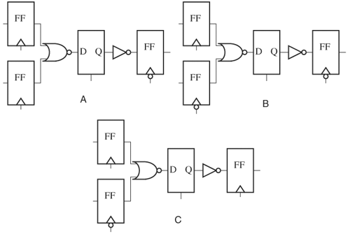
Cycle-based simulation simulates the circuit only at cycle boundaries so that all transitions in a cycle but the last one are ignored. In other words, cycle-based simulators compute the steady-state behavior. The following illustrates the difference between an event-driven simulator and a cycle-based simulator. Figure 2.11 shows the transitions in a clock cycle. For instance, node c has six transitions and node d has nine transitions. On the other hand, in an event-driven simulator, a gate needs to be simulated if one of its inputs changes value. (A smart event-driven simulator may simulate only if the input transition affects the gate’s output.) Therefore, gate A simulates five times; gate B, nine times; and gate C, six times, for a total of 20 times.

Because only the steady-state value is seen by the receiving FF, all the intermediate transitions can be ignored. Thus, in cycle-based simulation, the entire circuit is simulated just once, at the end of the current cycle. In this example, only three gates are simulated. In cycle-based simulation, all gates are simulated, regardless whether their inputs have changed. Therefore, an event-driven simulator is faster if there are few transitions, typically less than 5% active nodes. In practice, experiments confirm that a cycle-based simulator is almost always five to ten times faster.
For a circuit to be simulated by a cycle-based simulator, the simulator must be able to determine cycle boundaries (the beginning or the end of a clock cycle). It is for this reason that an asynchronous circuit cannot be simulated by a cycle-based simulator. The following is a list of properties that a cycle-based simulated circuit should possess:
No event or delay constructs can be simulated using a cycle-based simulator, because all events except clock transitions are ignored and delays are eliminated.
The clock tree must be made of only simple gates, such as
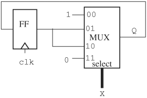
AND,OR, andINVERTOR, and the logic should be simple so that the simulator can determine the cycle boundary.False loops should be eliminated. A false loop is a loop that consists of combinational gates, but signals cannot propagate around the loop in any one cycle. An example of a false loop is shown in Figure 2.12. The loop is false because one of the multiplexors will select input
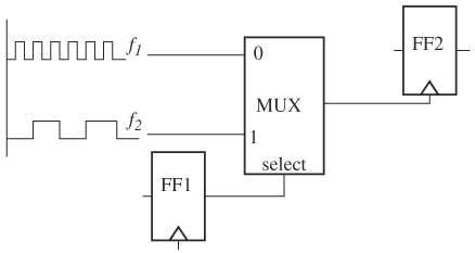
1, breaking up the loop. A false loop presents no problem to an event-driven simulator, because signal propagation will eventually die before traversing the loop, and hence the number of gates simulated is limited. But for a cycle-based simulator, it is not as straightforward when it comes to determining whether it’s a real combinational loop or a false loop, because absence of events is not used for terminating an evaluation. Furthermore, loops also really mess up static timing analysis.Clock gating needs special attention in cycle-based simulation, because the gating signal is not, in some simulator architectures, a part of the clock tree, but it can trigger a necessary evaluation. Let us consider the circuit segment in Figure 2.13, where the output of
FF1gates the clock ofFF2. Some simulators will only consider theANDgate as a part of clock tree forFF2, and will treatFF1and the buffer as a part of the data. Therefore,FF2is only evaluated on transitions ofclk2. However, if the output ofFF1toggles at different times than that ofclk2,FF2will not be evaluated at the transitions ofFF1, but these transitions do triggerFF2in a real circuit, causing simulation errors.Every sequential component must have a port connected to the system’s clock tree. This port is the clock to the sequential component and it triggers the evaluation of the component. A case in point is a frequency divider in which an output of an FF clocks another FF. If this condition is missing, incorrect simulation will result. Consider the sequential block
always @(x) out = x + y, wherexis not connected to a clock tree. In event-driven simulation, outputoutgets updated only whenxchanges. Supposeychanges value butxdoes not. Becausexis not connected to a clock tree, the block will not be evaluated, and hence outputoutstill has the old value ofy. However, in cycle-based simulation, the block is evaluated every cycle, and outputoutis updated with the latestxandyvalues regardless whetherxchanges. Consequently, an erroneous simulation occurs. Connectingxto a clock tree remedies the problem, because now an event simulator will evaluate the block whenever the clock, and thusx, changes.


Hardware simulators/emulators are special-purpose computers for accelerating circuit simulation/emulation. An emulator is like a simulator except that it is usually embedded in a system in the place of a subsystem; thus, response time is critical. Although the following discussion targets simulators, it is equally applicable to emulators. There are two categories of hardware simulators. The first kind uses FPGA chips to mimic the design. In the first kind of machine, a design is synthesized into a gate netlist, and then the FPGAs are mapped to the netlist and are programmed to the gate functionality. The second kind is based on special processors that directly simulate the circuit. Such a processor’s native language includes AND, OR, multiplexing, bit operations, and other Verilog operators so that a circuit is compiled to the processor’s machine code and is then simulated.
For hardware simulators there is an almost one-to-one correspondence between components in the design and the resource of the simulator. This is especially true for FPGA-type accelerators. Consequentially, loops are expanded and tasks and functions are inlined. In loop expansion, the body of the loop is duplicated N times, with respective values substituted for the loop indices, N being the loop count. Task/function inlining means that at every place where a task or function is called, the entire body of the task or function is inserted at the location. Therefore, a code segment of ten lines with three calls to a function of five lines expands to 7 + (3 * 5) = 22 lines.
It’s imperative to make an effort to minimize the body of loop statements, tasks, and functions. The idea of loop content minimization is demonstrated in the following example, which occurs often in practice, that searches for some patterns such as memory content and operates on the found items. It is very tempting to put everything under the search loop, as seen here:
found = 1'b0; // not found
for(i=1;i<=100;i=i+1) begin
   if(memory[i] == 8'b10101010 && !found) begin // search
      found = 1'b1;
      read = memory[i];
      do_lots_operations(read);// big task has 200 lines
   end // end of found
end // end of loop
When this loop expands, the 200 lines in task do_lots_operations are duplicated 100 times; the resulting code has around 20,000 lines! To minimize expansion size, search and operation steps should be made separate. A disjoint search and operation optimization produces the following code:
found = 1'b0; // not found
for(i=1;i<=100;i=i+1) begin
   if(memory[i] == 8'b10101010 && !found) begin // search
      found = 1'b1;
      read = memory[i];
   end // end of found
end // end of loop

if(found) do_lots_operations(read); // not duplicated
In this code, only the search portion is duplicated 100 times; the operations are not duplicated at all. The resulting code has about 500 lines, compared with 20,000 lines in the unoptimized case. If there is more than one item for which to search, the items can be packed into an array inside the search loop and later passed to the operation. This technique finds much application, especially in test benches.
Almost all hardware simulators delegate computing of C/C++ language routines, such as user tasks written with PLIs, to the host. When this happens, overhead time in passing the C/C++ routines to the host and then receiving the results back slow down the overall simulation. This is a major bottleneck in large system cosimulation. Therefore, PLI user tasks should be avoided at all costs. One strategy to mitigate performance degradation of PLI user tasks is to group them together and communicate with the host all at once (for example, at the end of a clock cycle). This strategy works well if the execution of all PLI user tasks can be delayed to the end of the cycle. One type of PLI user task, called midcycle PLI, cannot be delayed to the end of the cycle. These PLI user tasks return values that are used by other parts in the design in the same cycle. This drastically slows down simulation. Therefore, midcycle PLI user tasks should be treated, for practical purposes, as errors for hardware simulators.
Four-state (0, 1, x, and z) simulation has been in common use to detect design problems such as uninitialized states and bus contention in which the states and the bus are assigned x value. Value x denotes an unknown value and value z denotes high impedance. A simulator is a four-state simulator if every node can have a four-state value. A two-state simulator uses only 0 and 1 values. A two-state simulator is faster than a four-state simulator. If a node is uninitialized or a bus is in high impedance or contention, a two-state simulator maps x and z to either 0 or 1. It is common practice to simulate a design using a four-state simulator during the power-up stage until most nodes are initialized, then the design is switched to a two-state simulator for faster speed.
Because a real circuit does not compare or operate with x or z values, the design should never have x or z values (except for the case when x, z, and ? are used for synthesis purpose, which should be used with caution because this will give rise to discrepancies between a simulation model and a synthesis model); however, a test bench can have these values. A designer should take into consideration that the design along with the test bench may undergo two-state simulation as well as four-state simulation, and hence make an effort to minimize simulation result in discrepancies between the two. Some differences are inevitable, because of the inherent pessimism of x. Consider the two-to-one multiplexor with inputs that are both 1, but select x, as shown in Figure 2.14. The algebra of unknown x is that the complement of x is also x. Therefore, the inputs to the OR gate are both x, instead of x and ![]()
x for the multiplexor output. This is the result of a four-state simulation. However, in reality, because both inputs of the multiplexor are 1, the output should be 1 regardless of the select value.

If this multiplexor is simulated using a two-state simulator, the output will be 1, because the select value is mapped to 0.
Although inherent differences between four-state and two-state simulation exist, the designer should not allow these differences to propagate to create functional errors. Let us consider the following example:
if( FlipFlopOutput == 1'b0 ) begin
   count = count + 1;
end
Variable FlipFlopOutput, if uninitialized at power-up, takes on value x and thus makes the comparison false. In Verilog, a conditional expression is, by default, x if any one argument is x. Therefore, variable count does not increment. On the other hand, a two-state simulator represents an uninitialized variable with value 0, and hence satisfies the condition and increments variable count by one. Consequently, the values of count differ by at least one in two-state simulation and four-state simulation, and this difference can further penetrate into other parts of the design. This type of functional difference can be hard to debug and can be quite misleading.
The proper thing to do for this type of situation is to determine whether the inputs to the block (for example, FlipFlopOutput) should be initialized. If yes, make sure they are initialized; otherwise, closely examine your block to see how it should behave in reality, when the inputs can be either 0 or 1. Does it produce different results and propagate them to create different system states? If so, the designer needs to improve the design to be better immune to uninitialized states. Similar caution should be exercised about using strength.
As we discussed earlier, for style guidelines there is no clear division between error and warning. An error for a false loop in a cycle-based environment may be just a warning in an event-driven environment. Furthermore, there are various degrees of severity for errors and warnings. As a project progresses, a warning can be promoted to an error, and vice versa. Therefore, when implementing a linter, one should set the tool to have a user programmable error/warning system. For instance, it could issue seven levels of error and seven levels of warning, each corresponding to the categories in this chapter. It could have a command-line option to demote a class of error or to promote a class of warning.
Giving out warnings and errors is only the first step. The second step is to assist engineers to locate the code causing the warnings and errors. For some warnings and errors (such as combinational loops), the problematic code can be interspersed in several files. A graphical interface is helpful to show the connections among the code fragments. Keep in mind that a text-based interface is still required for the tool to be integrated into a verification flow.
In addition, a single root cause can generate multiple messages. For example, a false loop involving a bus can generate multiple loop messages, with each loop involving a particular bit. Conversely, an error can mask other errors; so, removing an error can unmask others and generate more. Both situations can be discouraging and misleading; therefore, a tool needs to limit the effects of these two extremes.
Finally, the program should postprocess warning and error log files, generate statistics, classify warning and error according to severity, and submit reports to responsible parties.
In summary, a good linting package has three components: a checker/linter that detects violations, a locator that assists users to locate the code causing the warnings and errors, and a report generator that creates reports and statistics.
Designing with verification in mind prevents errors from happening before the design goes into verification. One way to achieve this is to have a set of coding guidelines and a tool to enforce it. There are five general and three ad hoc categories—namely, functional, timing, performance, maintainability, and tool compatibility; plus cycle-based, hardware, and two-state simulation. A robust enforcement package should include a checker to detect violations, a locator to identify the problematic code, and a report generator to gather statistics. Errors and warnings are issued with predefined levels of severity and can be promoted or demoted as the project progresses.
1. | Find as many bad coding styles as possible in the following RTL code: reg [7:0] N, out;
reg [31:0] P;
reg [63:0] G;
reg [1:0] Y;
reg clock;
wire clk, enable;
assign clk = enable & clock;
always @(posedge clk) begin
Y = G[31:9] ^ N;
case (Y)
2'b00: Out = N;
2'b01: Out = N;
endcase
end
|
2. | What would a circuit be like if it were synthesized from the following code? always @(a or b) begin if(b == 1'b1 && a==1'b0) c = 1'b1; else if(b==1'b1 && a==1'b1) c = 1'b0; end |
3. | Determine whether the following RTL descriptions are sequential or combinational.
|
4. | Rewrite the following code as much as possible to conform to the preferred styles discussed in the chapter. and (out1, in1, in2);
or (out2, out1, in2);
2bitadder m1(carry_out,carry_in,in1,in2,out);
always @(posedge clock) begin
if(carry_out)
flag = 1'b1; // overflow
else if (~carry_out && carry_in) begin
check = 1; // a 1-bit flag
if(~out1) $display("do something");
end
else $call_PLI(carry_in, carry_out);
end
|
5. | As discussed in the chapter, bus contention should be checked at runtime with assertion routines.
|
6. | Identify all true and false loops in the Verilog code. You should treat an always @(c or b or d)
case (d)
1'b0: a = d;
default: e = b;
endcase
assign b = a;
always @(e or c)
d = e + c;
|
7. | Can the latch be replaced with a buffer in each of the cases in Figure 2.15, assuming that all latches and FFs are driven by the same clock? Explain. |
8. | Convert the following bit operations into bus operations without part selects: reg [31:0] A,B,C; B[15:0] = A[15:0] & |
9. | Minimize the following loop’s content. Suppose all loops must be unrolled and the routine must be expanded. What are the numbers of lines before and after you apply the optimization? done = 1'b0;
For(i=0;i<100;i=i+1) begin
if(!done && ((M[i] == 4'b1010) || (M[i] == 4'b1111))) begin
Do_massive_computation(M[i]); //1000 lines of code here
done = 1'b1;
end //end of if
end //end of for
|
10. | The following code has the so-called event-counting race. The intent is to count the total number of transitions on always @(Cx or Cy) C = C + 1; |
11. | Consider the circuit in Figure 2.16. The clock tree has a multiplexor that switches clock frequencies.
|