To simulate a design, an external apparatus called a test bench is often required to mimic the environment in which the design will reside. Among other functionality, the main purpose of a test bench, written in HDL, is to supply input waveforms to the design and to monitor its response. Because a test bench is not manufactured as the design, it has far fewer coding style restrictions. Together with the perception that test benches are discarded once the design is verified, the structures of a test bench are often at the mercy of verification engineers. Consequently, test benches frequently generate wrong stimuli, compare with wrong results, or miss corner cases, eventually diverting valuable engineering time to debugging the test benches instead of the design. Furthermore, without well-organized guidelines, test benches can be a nightmare to maintain and hence are not reusable. Therefore, to have easily maintainable and reliable test benches, it is important to understand organizations and designs of test benches.
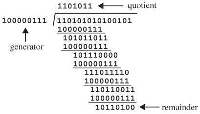
Through the process of creating a test bench for a simple circuit, we will see the major components of a test bench as a prelude to a systematic test bench architecture. Consider verifying a circuit computing the remainder for ECC CRC-8 with generator x8 + x2 + x + 1, whose coefficients are binary. The remainder from the generator is a polynomial of degree, at most, seven, and thus can be represented by a byte, whose bits are the remainder’s coefficients. For example, x7 + x5 + x2 + x + 1 is represented by 10100111. The circuit accepts a binary stream representing an arbitrary polynomial and computes the remainder divided by the generator. An example of binary division with this generator is shown in Figure 4.1. The input polynomial is x14 + x13 + x11 + x9 + x7 + x5 + x2 + 1. The remainder is 10110100, which is polynomial x7 + x5 + x4 + x2. The shift and subtract (exclusive OR in Boolean domain) operations are implemented using shift registers and XOR gates. A circuit computing a remainder using this generator is shown in Figure 4.2. The input stream is fed, MSB first, to port in of the shift register, which has a zero initial state. After the input is completely shifted in, the outputs of the FFs give the remainder. As a sanity check, shift in, MSB first, and byte 100000111, which is the generator itself. After eight cycles, the MSB appears at Q7 and is XORed with the last three 1 bits to produce all zeros at the FF outputs, giving a zero remainder, as expected when the generator is divided by itself.
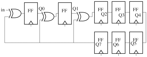
Let us call the RTL module for this circuit CRC8, with input ports CLK and IN, and output ports Q0, ...,Q7. The following line instantiates the design:
//design module instantiation
CRC8 DUV (.IN(in), .CLK(clk), .Q0(q0),..., .Q7(q7));
To set up a test bench for CRC8, we need to apply a bit stream to the circuit, which can be done by storing bits in an array and feeding the design from the array. Verilog code for this method of input application is shown here. At each rising edge of clk, the ith element of array input_array is fed to the input port in:
//apply input to CRC8 remainder circuit
initial i = size_of_input_polynomial;

always @ (posedge clk) begin
   if (i! = 0) begin
    in <= input_array[i];
    //input_array is binary representation of input polynomial
    // LSB is input_array[0]
    i <= i - 1;
   end // end of if
end
When the array is all shifted in i.e. i == 0, the outputs of the design are compared with the expected result. The expected result, the remainder, can be computed by dividing the input array with the generator using the modulo operator %. This remainder is compared with the outputs of the design. If they are unequal, a task is called to print out the error. Sample code for checking the response is
// compute and compare with expected result
remainder = input_array % 8'b10000111;
if(remainder != {q7,q6,...,q0})print_error();
Right after the circuit is powered up, the FFs should be initialized to zeros. This is done using an initial block. In this block, the FF outputs are initialized using assignments through hierarchical paths, such as DUV.Q0:
// initialize states to zero
initial begin
   DUV.Q0 = 1'b0;
   ...
   DUV.Q7 = 1'b0;
end
Finally, a clock waveform is generated to drive the design:
always clk <= #1 ~clk; // generate clock waveform
Putting these pieces together, with clock initialization, we have a test bench for CRC8:
//design module instantiation
CRC8 DUV (.IN(in), .CLK(clk), .Q0(q0),..., .Q7(q7));

// initialize states to zero and other variables
initial begin
   i = size_of_input_polynomial;
   clk = 0;

   DUV.q0 = 1'b0;
   ...
   DUV.q7 = 1'b0;
end

//apply input to CRC8 remainder circuit
always @ (posedge clk) begin
   if (i! = 0) begin
      in <= input_array[i];
      // input_array is binary representation of input polynomial
      // LSB is input_array[0]
       i <= i - 1;
    end // end of if
end

// compute and compare with expected result
remainder = input_array % 8'b10000111 ;
if(remainder != {q7,q6,...,q0}) print_error() ;

always clk <= #1 ~clk; // generate clock waveform
From this simple example, we see the six major components of a test bench, sometimes called a test harness:
Initialization
Input stimuli
Response assessment
Test bench-to-design interface
Clock generation and synchronization
Verification utility
The test bench-to-design interface, in the example, consists of access to the design signals through primary inputs, outputs, and hierarchical paths. Clock generation and synchronization, in the example, is just the clock generation. Verification utility is a collection of functions, tasks, and modules shared by various parts of the test bench, such as task print_error () in the example. The diagram in Figure 4.3 illustrates the organization and the components of a test bench.

In the previous example we assumed that the property to verify was that the CRC8 circuit calculates the correct remainder, given the initial state is zero. Another property that we could verify is that the circuit initializes correctly. (In this example, initialization is provided by the test bench. In a real design, initialization can be a part of the design. In that case, verifying correct initialization is more meaningful.) Still another property to verify is correct remainder calculation when input polynomials are “pipelined” into the circuit. Each of these properties, or scenarios, is called a test case. To illustrate the concept of a test case further, consider verifying an ALU. One test case can be verifying integer computations, while another test case verifies Boolean operations. Each of these test cases can have its own unique initial values, input stimuli, and expected responses. For example, to test integer addition and subtraction, input vectors could be chosen to cause overflow or underflow along with other corner cases; whereas in testing Boolean operations, certain bit patterns could be selected (such as alternating ones and zeros, or even or odd parity). Because multiple test cases use the same test bench, to maximize portability of a test bench, test cases must be separated from the test bench. To modify our example to extract the test case from the test bench, the initial values and input_array can be read from an external file (for example, using readmemb or readmemh) that contains a test case. A more in-depth discussion of this topic is relegated to a later section. Figure 4.4 shows a typical verification environment.

Initialization assigns values to state elements such as FFs and memories. Although a completed design has a circuitry that initializes on power-on, initialization is often done through a test bench for the reason that the initialization circuit may not have been designed at the time, or a simulation is to run starting from a time long after power-on so that simulating through the initialization stage will consume too much time, or the simulation emulates an exception condition that a normal operation of the design will not reach from its legal initial state.
Initializing can be done using test bench RTL code or PLIs. The former is usually reserved for designs with a small number of state elements or one in which accessing of state elements is relatively simple. The latter, for large designs in which the structure of the design is traversed to locate state elements (for example, enumerate all instantiated gates and blocks) is used to determine the sequential ones and apply corresponding initial values.
Initialization code, usually enclosed in initial blocks, assigns values to state elements using hierarchical paths. Although initial values can, in theory, propagate through the design’s primary inputs to the state elements, in practice the propagation sequences are difficult and time-consuming to generate.
One must decide whether to initialize a state element’s input or output. In most cases, outputs are initialized. If, for some reason, inputs are initialized, you should make certain that the values are not overwritten by the input logic cones. Furthermore, the time when initialization takes place needs to be determined, because not all initializations should occur at the same time or at the very first clock edge. For example, one cannot initialize a latch without knowing when the latch becomes transparent, because initializing when it is transparent runs the risk of having the initial values being overwritten. An example of initialization using test bench RTL code is shown here, in which some state elements in modules alu and usb are assigned initial values, and usb is initialized ten units of time later than alu:
initial
begin
   top.design.alu.multipler.ff9.Q = 1'b1;
   top.design.alu.multipler.ff9.Q_bar = 1'b0;
   ...
   #10;
   top.design.usb.xmit.latch3.Q = 1'b0;
   top.design.usb.xmit.latch3.Q_b = 1'b1;
   ...
end
Hard coding initial values makes the code unable to be reused if different initial values are often required for other test cases or the circuit requires initialization at a different time. To make it reusable, the code should be encapsulated inside a task with an input for initial values. In this way, whenever initialization is needed, the task is called. Applying this principle to the previous example, we can split the code into two tasks, one for alu and the other for usb:
task initialize_alu;
input [N:0] init_value;
begin
   top.design.alu.multipler.ff9.Q = init_value[0];
   top.design.alu.multipler.ff9.Q_bar = init_value[1];
   ...
end
endtask

task initialize_usb;
input [M:0] init_value;
begin
   top.design.usb.xmit.latch3.Q = init_value[0];
   top.design.usb.xmit.latch3.Q_b = init_value[1];
   ...
end
endtask
Now, to initialize, simply call the tasks with initial values:
initial
begin
   v1 = ...;
   v2 = ...;
   initialize_alu(v1);
   #10;
   initialize_usb(v2);
   ...
end
To see the power of reusable code, let’s make use of these tasks and readily implement a random initialization routine using Verilog’s system task $random(seed). It is highly recommended that the seeded version be used for repeatability. Note that $random(seed) returns a value with the size of an integer. So, if the input vector is of a different size, the returned value is scaled by the ratio of the maximum value of the input to that of the integer—namely, 2(a/b)—where a is the number of bits of the input and b is that of the integer. If the returned value is not scaled properly (such as linearly), the resulting distribution is changed:
task random_init;
input [K:0] seed;
begin
   reg [31:0] v1;
   reg [31:0] v2;
   v1 = $random(seed);
   v2 = $random(v1);
   initialize_alu(v1);
   #10;
   initialize_usb(v2);
   ...
end
endtask
Initializing memory is usually done by loading memory content stored in a file using system tasks $readmemh or $readmemb. System task $readmemh expects values in hex whereas $readmemb uses binary. For example,
$readmemh("filename",top.design.data_memory,'START_ADDRESS,
'END_ADDRESS);
Initialization codes cannot be synthesized (at the time of this writing) and usually are not supposed to be part of a library cell’s functionality. Thus, they should never be placed inside any library cells. Another reason for not putting initialization code inside a library cell is that different instantiations of the same cell may require different initial values. Besides, sometimes an instantiation without initialization is used as a means to verify initialization circuits. In any case, embedded initialization has detrimental effects and must be avoided all the time.
The aforementioned initialization method has several disadvantages. First, it produces a large amount of code in a large design, because an assignment is needed for every state element and memory. Second, explicitly specifying the state elements is not portable because the design can change, decreasing or increasing the number of state elements. To overcome these problems, a better mechanism should search for state elements and memory, and initialize them. Verilog does not offer a facility to perform this search directly, but PLI or VPI has routines to do just that, and more. Here we look at how sequential elements can be initialized using PLIs.
For simplicity, let’s consider only FFs. However, the algorithm can be generalized to other types of state elements. First, all gates in the design are enumerated and each gate is checked for sequential or combinational type. If a sequential gate is found, all its outputs are then iterated, and each output is assigned an initial value, which is, for example, retrieved from a database. These procedures are facilitated by the acc routines of PLI. For a complete description of PLI and its applications, refer to The Verilog PLI Handbook: A User’s Guide and Comprehensive Reference on the Verilog Programming Language Interface by Stuart Sutherland. C pseudocode for initializing FFs using PLI is as follows:
 void initialize_flip_flop ( ) {
    ...
    db = fopen("database","r");
    module = acc_fetch_by_name("my_design");
    cell = NULL:
    while(cell = acc_next_cell(module, cell ){
       if(cell is sequential){
          port = acc_next_port(cell, port);
       if (port is output) {
            get_init_value(db, port, &value);
            acc_set_value(port, &value, &delay);
          }
       }
    }
 }
The first acc routine gets the handle of the design by name, assuming the module name of the design is my_design. The second acc routine, acc_next_cell, iterates through all cells in the design (in other words, each call to this acc routine returns a cell in the design until it runs out, and then it returns NULL to exit the while loop). If the cell is sequential, acc_next_port iterates all its ports. For each port, its polarity is checked. If it is an output, the initial value for the output is retrieved from a database using function get_init_value. Function get_init_value is a user function that searches the initial value for a port in database db. Once found, the value is assigned to the port using acc routine acc_set_value.
This C code is compiled into object code and is linked to a Verilog user-defined task, say $init_FFs. The thread of execution during a simulation run is shown in Figure 4.5. The RTL code runs on a simulator and the C object code runs on the host. When $init_FFs is encountered during simulation, the simulation is paused and control is passed to the host system to execute the compiled PLI C code, in which all cells in the design are traversed using PLI’s acc routines and sequential gates are processed. Outputs of each sequential cell are iterated and assigned initial values stored in a database. When the PLI C code is finished, all FF outputs have been initialized. Then the control is passed back to the simulator, and simulation resumes.

Initializing a variable at time zero requires care, because the change from an unknown value before time zero to the initialized value at time zero can constitute a transition for some simulators, whereas other simulators will not pick up this transition. Therefore, inconsistent results are produced from simulator to simulator. To avoid this, one strategy is to initialize at a positive time, and treat this time as the time of origin. Sometimes it is safer to initialize explicitly to the unknown value x at time zero, followed by an initialization to the desired values at a later time. For example,
task init_later;
input [N:0] value;
begin
   design.usb.xmit.Q = 1'bx; // avoid time zero event
   ...
   #1;
   design.usb.xmit.Q = value[0]; // now real initialization
   ...
end
endtask
Clocks are the main synchronizing signals to which all other signals reference. In a majority of situations, clock waveforms are deterministic and periodic. Therefore, if you know how to write RTL code for one period, the complete waveform can be generated by embedding the one period inside a loop. To create one period of clock, there are two methods: explicit and toggle. With the explicit method, you specify rising and falling times of the clock and assign a value to it at each of the transition times. With the toggle method, you also specify rising and falling times of the clock, but invert the clock at the transition times.
Consider generating the clock waveform in Figure 4.6. First, one period of a clock is generated. Using the explicit method, one period of clock has the RTL codes
#1 clock = 1'b1;
#1 clock = 1'b0;
#2 clock = 1'b1;
#2 clock = 1'b0;

The delays before the assignments are delay intervals between successive transitions. Putting this period inside a loop and initializing the clock produces the complete waveform, as shown here:
initial clock = 1'b0;
always begin
   #1 clock = 1'b1;
   #1 clock = 1'b0;
   #2 clock = 1'b1;
   #2 clock = 1'b0;
end
The same clock waveform can also be generated using the toggle method:
initial clock = 1'b0;
always begin
   #1 clock = ~clock; // rising
   #1 clock = ~clock; // falling
   #2 clock = ~clock; // rising
   #2 clock = ~clock; // falling
end
This toggle method can be difficult to see the value of clock at a given time. Thus, comments indicating rising or falling transitions are recommended. Furthermore, if the clock is left uninitialized, the clock will not toggle and simply stays at the unknown value x—a potential pitfall that the explicit method avoids. On the other hand, the toggle method is easy to change the phase, or the initial value, of the clock by simply initializing the clock to a different value while keeping the toggle statements intact. Changing a clock’s initial value is more complicated with the explicit method; all assign values have to be modified.
Note that we used blocking assignment operator =, but nonblocking operator <= could also be used in this example.
In the previous example, the delays are interval delays between successive transitions, and there are situations when absolute transition times are desired. To do so, nonblocking intraassignment delay can be used. The following code representing the waveform shown in Figure 4.6 uses nonblocking intraassignment delays:
initial begin
   clock <= #0 1'b0;
   clock <= #1 1'b1;
   clock <= #2 1'b0;
   clock <= #4 1'b1;
   clock <= #6 1'b0;
   clock <= #7 1'b1;
   ...
end
Statement clock <= #2 1'b0 assigns 1'b0 to clock two units of time from the current time. Because this statement does not block, the next statement is simulated immediately. The next statement, clock <= #4 1'b1, assigns 1 to clock four units of time from the current time. Therefore, all delays in the nonblocking assignments refer to the current time.
Because the delays are absolute transition times, all transitions have to be explicitly specified, as opposed to embedding one period in a loop. Hence, generating waveforms using absolute times is used only for aperiodic waveforms such as reset signals. It’s important to note that if the nonblocking assignments are replaced by blocking assignments, the next statement must wait until the current statement is executed, meaning the delays now have become interval delays.
Similar to the time zero initialization problem, the very first transition of clock at time zero may be perceived as a transition because clock has an unknown value before time zero and gets assigned to a value at time zero. Whether this time zero transition is perceived is simulator dependent, and thus care must be exercised to deal with either scenario. One way to avoid this ambiguity is to initialize clock explicitly to unknown value x at time zero, hence eliminating the time zero transition, and start the clock at a later time.
During verification, the clock period or duty cycle may change. It is beneficial to use parameters to represent the delays, instead of hard coding them. For example, to generate a clock starting with zero that has a 50% duty cycle, one may code as follows:
define PERIOD 4
initial clock = 1'b0;
always #('PERIOD/2) clock = ~clock;
Caution should be exercised when PERIOD is not evenly divided by two. If PERIOD is odd, the result is truncated. If integer division is replaced by real division, the result is rounded off according to the specified resolution.
In Verilog, the unit for delay (for example, #3) is specified using 'timescale, which is declared as
'timescale unit/resolution
where unit is the unit of measurement for time and resolution is the precision of time. For example, with 'timescale 1.0ns/100ps, # (4/3.0) clock = 1'b1 means at 1300 ps, clock is assigned to 1. Note that although 4/3.0 gives 1333ps, it is rounded off to 1300ps because the resolution is declared to be 100ps.
A complex chip often uses multiple clocks generated from a phase lock loop (PLL) block. The analog behavior of PLL is not modeled in HDL, but is abstracted to generate clock waveforms using delays and assigns. When multiple clock waveforms are generated, their relationship needs to be determined (for example, whether their transitions are independent, whether some clocks are derived from others). A clock can be derived from another via a frequency divider or multiplier. If the frequency ratio is an integer, it is easy to generate a derived clock from the base clock. For frequency division, the derived clock can be generated from base clock without knowing the base clock’s frequency. To divide base_clock N times to get derived_clock, trigger a transition on derived_clock for every N transitions of base_clock:
initial i = 0;

always @( base_clock ) begin
i = i % N;
if (i == 0) derived_clock = ~derived_clock;
i = i + 1;
end
Multiplying a clock frequency by N can be achieved using Verilog’s repeat statement once the base clock’s frequency is known (for example, for every positive or negative transition of the base clock, repeatedly generate 2N transitions for the derived clock). For example,
always @(posedge base_clock) begin
repeat (2N) clock = #(period/(2N)) ~clock;
end
If the period of the base clock is not known or is changing constantly, and/or the ratio is not an integer, a different technique is required. First, the base clock’s period is measured on the fly and then the derived clock is generated using
forever clock = #(period/(2N)) ~clock;
A sample code to implement this general clock divider/multiplier is as follows:
// measure the first period of base_clock
initial begin
derived_clock = 1'b0; // assume starting 0
@(posedge base_clock) T1 = $realtime;
@(posedge base_clock) T2 = $realtime;
period = T2 - T1;
T1 = T2;
->start; // start generating derived_clock
end

// continuously measure base_clock's period
always @(start)
forever
@(posedge base_clock) begin
T2 = $realtime;
period = T2 - T1;
T1 = T2;
end

// generate derived_clock N times the frequency of base_clock
always @(start)
forever derived_clock = #(period/(2N)) ~ derived_clock;
Make sure that the proper time scale is used so that the division of the period by 2N has the correct precision.
If the clocks are independent, each of them should be modeled with its own always statement. For example, the following code generates two independent clocks:
initial clock1 = 1'b0;
always clock1 = #1 ~clock1;

initial clock2 = 1'b0;
always clock2 = #2 ~clock2;
An incorrect way to produce these two clocks is to use one clock to generate the other, as illustrated here:
initial clock1 = 1'b0;
always clock1 = #1 ~clock1;

initial clock2 = 1'b0;
always @ (negedge clock1) clock2 = ~clock2;
Although any waveform viewer shows that this set of clocks has the same transitions as the previous set, they are fundamentally different. clock2 of the second set is synchronized with clock1.
To emphasize more the relative independence of two clocks, jitter can be introduced to one of the clocks to simulate the nondeterministic relative phase. This can be done with a random generator:
initial clock1 = 1'b0;
always clock1 = #1 ~clock1;
jitter = $random(seed) % RANGE;
assign clock1_jittered = #(jitter) clock1;
The modulo operator % returns the remainder when divided by RANGE, and thus restricts the range of jitter. Clock clock1_jittered is a version of clock1 with edges that are randomly shifted in the range [0, RANGE]. All random functions/tasks should be called with a seed so that the result can be reproduced later when errors are found. Verilog offers a variety of random distributions, such as uniform, normal, and Poisson.
Because independent waveforms are not locked in phase, they can drift relative to each other. Jittering models this phase-drifting phenomenon. When two independent waveforms arrive at the same gate, glitches can come and go depending on the input’s relative phase, creating intermittent behavior. Therefore, independent waveforms should be first synchronized before propagation. A synchronizer uses a signal, the synchronizing signal, to trigger sampling of another to create a dependency between them, hence removing the uncertainty in their relative phase. The following code is a simple synchronizer. On every transition of signal fast_clock, signal clock1 is sampled. The synchronizer is essentially a latch; thus, nonblocking assign is used to avoid a race condition:
always (fast_clock)
   clock_synchronized <= clock1;
If the synchronizing signal’s transitions do not align with those of the synchronized signal, some transitions will be missed, as shown in Figure 4.7. Because transitions will be missed if the synchronizing signal has a lower frequency, the signal with the highest frequency is usually chosen as the synchronizing signal.

Because of the nonblocking assign in the synchronizer, the synchronized signal and the synchronizing signal are not exactly aligned but are separated by an infinitesimal amount. This is the result of a characteristic of nonblock assignment. At simulation time, nonblocking assignments are evaluated after all regular events scheduled for the time are evaluated. For example, in the following RTL code, the value of v is sampled when the nonblocking statement is encountered, but the actual assignment to x happens only after all blocking statements are evaluated. In this case, x gets the value of v after the blocking assignment y = x is executed. Thus, y gets the old value of x (the value of the previous clock cycle). Therefore, even though the two assignments are evaluated at the same simulation time, y always lags x by one clock cycle:
always @(posedge clock) begin
x <= v;
y = x;
end
In the previous synchronizer example, the synchronized signal, clock_synchronized, always lags synchronizing clock1 by an infinitesimal amount. This amount is from the time clock1 is sampled to the time clock_synchronized is actually assigned. Nevertheless, the two clocks’ transitions always have identical simulation times. However small this infinitesimal amount is, it sometimes can cause other signals to lag by a cycle, as illustrated in the previous example.
A central clock module generates various clock waveforms from the same clock source. During circuit implementation, the clock source is a PLL, and various clock signals are derived from the PLL output. In RTL, clock generation should be encapsulated as a module with parameters to change clock frequencies, phases, and jitter ranges, among others. A typical block diagram for a clock generation network is shown in Figure 4.8. The primary clock source is a simple waveform generator, modeling a PLL. The secondary clock generation block derives clocks of various frequencies and phases with frequency multipliers, dividers, and phase shifters. Frequency, phase, and random distribution are controlled through parameters and variables. Finally, the clock distributor multiplexes the clocks to appropriate clock domains. In RTL, the clock generation network is

module clock_generation_network (clk1, clk2,...);
output clk1, clk2,...;
parameter DISTRIBUTION 1;
parameter JITTER_RANGE 2;
...
primary_clock pc (.clock_src(csrc));
clock_gen cg(.in_clock(csrc),.freq1(freq1),.phase1(.ph1),...);
clock_distributor cd (.outclk1(clk1),..., .inclk1(freq1),...);

endmodule
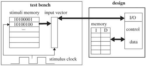
Many ways exist to apply input vectors to the design under verification. Let’s start with the most basic method: Assign vectors to the primary inputs of the design synchronously. A block diagram illustrating this method is shown in Figure 4.9. Vectors are stored in stimuli memory. Triggered by a stimulus clock, memory is read one vector at a time and is assigned to an array. The array is then applied to the design’s primary inputs. A sample RTL test bench implementing this method is as follows:
reg [M:0] input_vectors [N:0] // stimulus memory
reg [M:0] vector; // input vector

initial
begin
  $load_memory (input_vectors, "stimuli_file");
  i = 0;
end

always @(posedge stimulus_clock)
begin
  if(apply_input == TRUE) begin
    vector = input_vectors[i];
    design.address <= vector[31:0];
    ...
    design.data <= vector [M:M-31];

    i = i + 1;
  end
end
The initial block loads memory input_vectors from file stimuli_file, which holds all stimulus values, and resets counter i. Variable apply_input is controlled elsewhere in the test bench and is TRUE when the design is ready to accept stimuli.
Clock stimulus_clock, not part of the design, models the external clock that the design is seeing, and should be synchronized to the design’s clock. Furthermore, the assignments to the design’s primary inputs should be nonblocking; otherwise, race problems may result, as demonstrated in the following simple example. The design is a DFF and the stimulus clock is the same as the FF clock:
// design under verification, a D-flip-flop
always @(posedge clock)
  Q <= D;

// test bench that applies stimuli to design's primary inputs
always @(posedge clock)
begin
  D = vector[0]; // creates race
  i = i + 1;
end
On the positive transition of the clock, the following two events are scheduled: the sampling of value D to be applied to Q, and the assignment to D from vector[0]. The execution order of these two events is not specified in the Verilog IEEE standard and hence is at the mercy of the simulator. This order of execution affects the value D sampled. If sampling of D is executed first, Q will be assigned the value of D from the previous cycle. If assignment to D is first, Q will have D’s current value; hence, a race problem has occurred. Note that the use of a nonblocking assignment in the design does not prevent this race problem. However, using a nonblocking assignment in the test bench eliminates it.
The always block in the previous example explicitly ties the stimulus memory to the design’s primary inputs. This is not very flexible or portable, because the always block cannot be used to apply stimuli from other memory or to apply the same memory to another design. To remedy this, the code can be encapsulated as a task that has an input to accept a vector so that whenever a stimulus needs to be applied, the task is called with the stimulus as the input. Furthermore, one such task is associated with each design so that to stimulate the design, the design’s task is invoked. In this way, stimulus application is separate from particular memory or design, and it is self-contained, reusable, and portable. The following example demonstrates this technique in applying a reset sequence:
// task applying an input to cpu's PIs
task cpu_apply_input;
input [N:0] vector;
begin
  cpu.address = vector[0];
  ...
  cpu.data = vector[j];
  ...
  cpu.interrupt = vector[k];
  ...
end
endtask

initial // use the cpu task to apply inputs
begin
  #10;
  cpu_apply_input(64'b0); // reset
  ...
  #50;
  cpu_apply_input(v1); // now start input vector sequence
  #60;
  cpu_apply_input(v2);
  ...
end
Besides loading stimulus vectors from a file to memory and iterating the memory to apply input vectors, stimuli can be generated on the fly via a task, a function, a PLI user task, or a random generator. Code using these methods is similar and can be encapsulated in a task such as cpu_apply_vector, as in the previous example. Let’s look at some sample implementations.
In the first implementation, the task accepts an index indicating the vector is to be applied to the input and assigns the vector to it. The indexed vector is obtained through another task generate_vector:
task apply_vector_task; //apply vectors from a task
input index;
output [N:0] primary_input;
reg [N:0] vector;
 begin
   generate_vector(index, vector); // generate indexed vector
   primary_input <= vector; // apply vector
 end
 endtask

always @(start) // on start, call apply_vector_task
begin
  #10;
  apply_vector_task(i, top.cpu.inputs);
  i = i + 1; // next vector
end
In the second implementation, the vector-generating task is replaced by a PLI user task, which computes the indexed vector in C/C++. The user task, when encountered in RTL, calls the C/C++ routine and returns with the vector:
task apply_vector_PLI; //apply vectors from a PLI
input index;
output [N:0] primary_input;
reg [N:0] vector;
begin
  $gen_vector_PLI (index, vector); // generate indexed vector
  primary_input <= vector; // apply to
end
endtask
In the third implementation, random vectors are generated using Verilog’s system task $random:
task apply_vector_random; // apply random vectors
input [32:0] seed;
output [N:0] primary_input;
begin
  primary_input <= $random(seed); // gen. random vector
end
endtask
All the previous examples clock input vectors into the design’s primary inputs. There are situations when no clock is available and input stimuli are applied based on other events. An example is CPU data and instruction memory that sends bytes only when the CPU requests them. Another example is an asynchronous I/O specification, which often exists during the early stage of design, such as the one shown in Figure 4.10. When the sender is armed, 4 bytes of data are sent to two receivers. When the sender finishes transmitting, a done event is sent to the receivers, which in turn disable the ready signals and proceed to process the data.
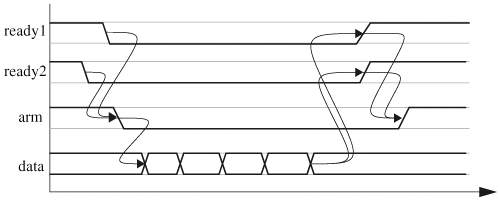
Let us write a stimulus generator to model the specification in Figure 4.10. There are two components in the test bench. The first one decides whether both receivers are ready and, if so, activates an arming signal. The other component sends out blocks of data when armed and notifies the receivers when done. Lowering or raising signals ready1 and ready2 is the receivers’ responsibility. When the receivers are ready to get data, they enable, lower the ready lines, and snoop on the bus for data. In addition, the receivers also monitor signal done. When signal done is activated, the receivers wrap up data retrieval and disable the ready signals by raising them:
always // detects whether receivers are ready
begin
  @(ready1 or ready2)
  arm = ready1 | ready2; // arm when both are ready
end

always @(negedge arm)
begin
  transmit_data();
  -> done; // notify receivers after data are transmitted
end
In large designs, working at the bit level is difficult to manage. Vectors at the bit level are not intuitive to the functions they represent. Therefore, functional coverage (that is, how much the design is tested) is hard to determine. In addition, generating random bit-level vectors is prone to generating illegal operations. An alternative is to elevate stimuli to the instruction code level. This method is especially attractive for designs that operate from instructions, such as processors.
Using the programmed stimuli method, the memory holding the stimulus vectors is a part of the design—instruction and data memory. A test, described by a programming language such as C/C++ or Assembly, is compiled into the design’s machine code and is then loaded into instruction and data memory. After the memory is loaded, the design is started to run off the memory. This process is depicted in Figure 4.11.
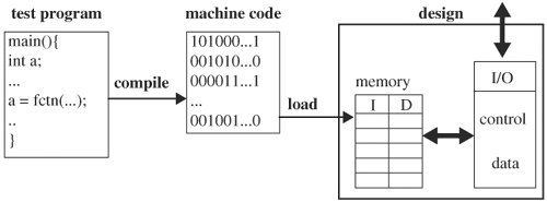
A major advantage for programmed code verification is its convenience of generating large tests. These tests can be as close as possible to real applications intended to run on the design. The main drawback is that a tool chain is required. The tool chain consists of a compiler, an assembler, a loader, and possibly a disassembler and a debugger.
To determine whether a simulation ends correctly, a high-level software simulator of the design is constructed to run the same instruction code. The results from the high-level simulator are then compared with the RTL ending states. If a high-level simulator is not available or is difficult to design, checking the RTL simulation results can be difficult with this method. This strategy of running a high-level design simulator along with the design’s RTL model is sometimes called cosimulation.
Simulations based on programmed code usually run for many cycles, because the programs or test cases are often large. Therefore, debugging is a challenge.
The general principle in assessing simulation results consists of two parts. The first part monitors the design’s nodes during simulation, and the second part compares the node values with expected values. A discrepancy warrants an in-depth investigation, and the cause could be a real design bug or a bug in the specification. Absence of discrepancies could have many meanings. It could mean that the erroneous nodes were not monitored, bugs were not exercised by the input stimuli, there are bugs in the expected values that mask the real problems, or the design is indeed free of bugs.
Comparing simulation results with expected values can be done on the fly or off-line. With the on-the-fly method, node values are gathered during the simulation and are compared with the expected values. With the off-line method, called postprocessing, node values are dumped out to a file during simulation, and the file is processed to find discrepancies after the simulation is finished. In this section, we start with postprocessing method, followed by self-checking routines, and conclude with techniques for checking temporal specifications.
State dumping prints node values to a file during simulation. With dumping on, simulation speed is drastically decreased, from 2 to 20 times. Thus, in practice, simulation performance requirements prohibit dumping out all nodes in the design. With access only to a part of design, it is necessary to use other measures to locate bugs effectively. Some such measures are to restrict dumping to certain areas where bugs are more likely to occur, turn on dumping only within a time window, dump out signals only at a specified depth from the top module, and sample signals only when they change. These features—scope, interval, depth, and sampling, should be configured in a well-designed dumping routine.
Scope refers to the range of signals to be printed out. A scope can be the Verilog scopes (such as module, task, function, and named block) or a user-defined scope, which can be a group of functionally similar modules. To say that a scope is to be “dumped out” is to print out all signal values within the scope. For example, if the scope is a module, then dumping out that scope prints out all node values inside that module. In a user-defined scope, arbitrary modules can be grouped together as a scope. In practice, these modules usually form a functional unit. The following code is a user-defined scope consisting of modules A and B. Dumping of this scope is activated by defining PRINT_IMAGE:
'ifdef PRINT_IMAGE
  $display("top.A.n1 = %b, ... ", top.A.n1, ...) ;
  ...
  $display("top.B.m1 = %b, ... ", top.B.m1, ...) ;
  ...
'endif
Explicitly indicating the nodes to be printed is a tedious task and is error prone. A better way is to write a user task, $dump_node, that takes in a path to a module and dumps out all the nodes inside the module. For example,
'ifdef PRINT_IMAGE
  $dump_nodes(top.A) ;
  $dump_nodes(top.B) ;
'endif
There are two ways that the scope of dumping can be controlled. The first method uses the ifdef directive, as shown in the previous example. In this case, the decision to dump (or not) is made before compilation time. If it is not defined, the code within the directive is excluded from compilation. Thus, if the ifdef directives are disabled, the compiled image is smaller and thus runs faster; however, the decision to disable dumping cannot be reversed later during simulation runs. The other method uses a runtime argument to turn dumping on or off through the use of plusargs. In this case, the entire design together with the dumping routines is compiled, resulting in a larger image. However, the set of signals to be dumped can be adjusted during simulation, resulting in dumping fewer irrelevant signals and better overall simulation performance. An example of using plusargs is
if($test$plusargs("dump_on"))
begin
  $dump_nodes(top.A) ;
  $dump_nodes(top.B) ;
end
To turn on dumping during simulation, the following command can be used:
simulate +dump_on ...
The plusargs +dump_on is checked by $test$plusargs("dump_on"). In this case, $test$plusargs returns true, and modules A and B are dumped out.
We have been referring to dumping out nodes inside a module. What does this really mean? If a module has instantiations of other modules, are the nodes inside these modules to be dumped out too? This brings up the question of depth. A convention is that depth is one plus the maximum number of module boundary a node has to cross downward from the dumping scope. Using $dump_nodes (top.A) as an example, the dumping scope is module A. Because all nodes inside module A can be reached without going through any module boundary, all these nodes have depth 1. If module A has a module instantiation, such as instance1, all nodes inside module mod1 are one module boundary down from the dumping scope A. Therefore, nodes inside instance1 are of depth 2:
module A; // dumping scope
  ...
  mod1 instance1(...); // one level down
  ...
endmodule

module mod1(...)
begin
  ...
endmodule
If depth N is specified in dumping, it means all signals of depth not greater than N, as opposed to only the signal of depth N. If nodes of all depth are to be dumped, the depth is defined to be 0. With the concept of depth introduced, $dump_nodes can be enhanced to include an argument for depth, and you can only dump out signals of the required depth (for example, $dump_nodes(top.A, depth)).
Oftentimes, signal traces are needed only during a certain time interval. For large designs (for example, an entire CPU), it is rare that signals are dumped out right from the start of the simulation to the end of the simulation. Tracing signals for the entire simulation run, even when it is needed only for a small time interval, slows down simulation drastically and wastes a large amount of disk space. Therefore, dumping tasks or routines should have parameters to turn on and off. For example, $dump_nodes can be modified as shown so that signals are dumped when variable dump_on is 1:
$dump_nodes(top.A, depth, dump_on) ;
With this on/off switch, nodes can be traced contingent on circuit state. For example, if a forbidden state is reached, dump_on can be set to 1 to start tracing problems:
$dump_nodes(top.A, 0, bad_state_reached) ;
When a signal is dumped, how often should it be sampled? A common practice is to sample signals with respect to a clock. For example,
always @(clock)
   $display("signal = %d", signal) ;
There are several problems with this sampling technique. First, if the signal’s transition does not line up with the clock transitions, the signal’s change will show up only at the next clock transition; that is, the dump data will not show the time the signal changes, but will show the time the change is sampled by the clock. Second, if the signal does not change often, many samples would be redundant. Third, in a design with multiple clocks, choosing a reference clock creates confusion. To solve these problems, a signal should be sampled only when it changes. Verilog provides such a facility called $monitor.$monitor takes in a list of signals as arguments and prints out the signals whenever they change. Furthermore, $monitor can be turned on with $monitoron and off with $monitoroff. Dumping changes only also increases simulation performance, because the I/O file is very slow compared with the simulation. An example of using $monitor is as follows:
initial monitor($time, "a=%b,b=%d,...",A,B, ...) ;
// whenever signal A, B, ... changes, time stamp and the
// signal list will be printed
...
if (initialization) $monitoroff;
// turn off display during initialization
...
if (start_design) $monitoron;
// turn on display in running the design
...
$monitor is executed whenever any variable, except $time, changes. $monitor needs to be instantiated just once, and it will be in effect for the entire simulation run, as opposed to $display, which is called whenever something is to be printed. Therefore, monitor should reside in an initial block.
By default, signals are printed to the screen in the format specified (for example, in $display or $monitor). When the amount of data is large, formats more compact than text are used. These formats are usually proprietary and require a software program, called a waveform viewer, to be viewed. Therefore, text format is still used for small-scale signal tracing, mainly for its convenience. A common text format is VCD (or value change dump).
This format records only the times and values of signal changes. A simplified sample VCD file is
...
$var reg 8 *@ busA $end
$var reg 8 *# busB $end
...
#100
$dumpvars
bx*$
bx*#
...
$end
#200
00101111*@
11110000*#
...
#300
10101010*@
00001010*#
...
The first two lines associate buses busA and busB with symbols *@ and *# respectively. The reason for this abbreviation is to use shorter names for the original names so that file size can be reduced. The first time stamp is at time #100. The keyword $dumpvars lists all the variables and their initial values. Note that the short names are used instead of the original names. The future time stamps start with # (for example, #200 and #300). The lines following #200 are the values for *@ and *#. For example, at time 200, busA has value 00101111 and busB has value 11110000.
IEEE Verilog standard 1364-1995 provides a suite of VCD dumping system tasks. These tasks are $dumpfile, $dumpvars, $dumpon, $dumpoff, $dumpall, $dumplimit, and $dumpflush. $dumpfile (“file”) specifies the name of the dump file. $dumpon and $dumpoff turn on and off dumping. $dumpvars (depth, scope) dumps out variables in the scope at the specified depth. If it is used without arguments, all variables are dumped. $dumplimit(size) limits the size of the dump file. $dumpall creates a check point or a snapshot of all selected variables. $dumpflush empties the VCD file buffer to the dump file. Sample code using the dump system tasks is as follows:
initial
begin
  $dumpvars(0,top.design); // dump everything in design
  $dumplimit(100,000,000); // limit file size to 100MB
end

always @(start_dump)
begin
  $dumpon;
  repeat (1000) @(posedge clock)// dump 1000 cycles
  $dumpoff;
end
Signals are dumped out for either detecting bugs or debugging bugs. To detect bugs, the signal traces are visually inspected, viewed with a waveform viewer, or compared with a known, good output. Visual inspection is suitable only for dealing with a small number of signals. Viewing with a waveform viewer is the main route for debugging a problem when the user knows where to look for clues and causes, and thus the scope of interest is narrow enough to handle manually. In detecting bugs, especially in large designs, the entire set of dumped traces needs to be examined, and thus manual inspection is not feasible. A common method to detect bugs is to compare signal traces with a set of known, good reference traces. These reference traces are also called the golden response. Comparing a set of traces and the golden response can be done using the UNIX diff command if the format is text; otherwise, a waveform comparator must be used. The comparison is fully automatic and can easily handle large numbers of traces.
A golden response can be generated directly from the specification or can be generated by a different model of the design (for example, a nonsynthesizable higher level model or a C/C++ model). If there are differences between a set of traces and the golden response, the causes can be design bugs or bugs in the golden response, that is, bug in specification.
The following design demonstrates how a golden response is generated. This design has two 32-bit inputs and one 32-bit output. If we suppose this design is a reference model, then the values of its variables can be used as a golden response. If we deem it sufficient to compare only the inputs and the output, then the $fdisplay statement creates a golden response. To create a golden response, the design is simulated on a number of tests and each run prints out the I/O values, which constitute a golden response. In this example, the file named gold_file contains a golden response.
module reference_model (in1, in2, out1);
input [31:0] in1;
input [31:0] in2;
output [31:0] out1;
integer fp;
  ...
'ifdef GEN_GOLDEN_FILE
  initial fp = $fopen ("gold_file");
'endif

...
'ifdef GEN_GOLDEN_FILE
always @(posedge clock)
  $fdisplay(fp, $time, "in1 = %d, in2 = %d, out1 = %d", in1,
in2, out1);
'endif

  ...
endmodule
A sample output produced by simulating above is
...
1012 in1 = 121, in2 = 92, out1 = 213
1032 in1 = 32, in2 = 98, out1 = 124
...
What variables should be printed in a golden file? Are I/O ports sufficient? The answer depends on the design. I/O ports are the minimum. Printing every node is overkill and often is not feasible because the reference model and the design usually do not have the same internal nodes. If state variables are well defined in the reference model, they should be included in the golden response. Besides variable selection, the time stamp should be included in most cases. Furthermore, the time window in which traces should be considered valid is another judgment the user needs to make. The wider the window, the more coverage it provides, and the more time and disk space it consumes.
Golden responses do not usually remain invariant throughout the design cycle. Specifications can change and, more often than not, the dumping formats or variables change. In either case, the golden responses need to be regenerated. Moreover, golden responses very often need to be augmented to record new stimuli and responses, and there are practically infinitely many stimulus-and-response pairs. Even if a design’s responses match the golden responses, they may not meet other design requirements not dictated by golden responses (examples of which include power, area, and testability constraints). This means that the design will change and may alter its responses, even the reference model’s responses. In summary, in practice, golden files need to be updated constantly as the project progresses.
An advantage of using golden files is its simplicity for comparison. There are several drawbacks. The first one is maintenance. If a bug is found in the supposedly correct design, the design is changed to meet other constraints, the specifications are changed, or the printing formats or variables are changed, all golden files must be updated. In a large design, thousands of golden files are typical. Furthermore, golden files can be very large, especially in long simulation runs with many signals dumped out; gigabytes of golden files are commonplace. Their large size costs disk space and presents problems for maintenance.
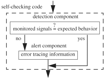
Dumping out signals and comparing with golden files have costly performance hits; file I/O can easily slow down a simulation by a factor of 10x or more. Even when there are no bugs in the design, large amounts of data are still dumped out. To avoid dumping signals, checking is moved to the test bench so that signals are monitored and compared constantly against expected behavior. This technique is called self-checking. The general structure of self-checking codes consists of two components: detection and alert. The detection component compares monitored signals with expected values. This component can be further divided into two parts: The first part collects the monitored signals at specified intervals, and the second component provides the expected behavior.
Collecting signals in most cases is simply accessing the signals by using hierarchical paths. If comparison is written as a task that takes in monitored signals as arguments, the signals need to be packed as an array before calling the comparison task. As an example,
// pack monitored signals into an array
signal_array[0] = top.design.fpu.mm1.q;
signal_array[1] = top.design.mmu.tb1.q;
...
signal_array[N] = top.design.xmt.regf.q;

check_signals (signal_array); // comparison task
Checking a memory’s contents often requires preprocessing: Search and package the desired entries into an array before calling the checking routine. In the following example, memory I_mem contains instructions, and the instructions retired at the end of the simulation have the MSB set. Before checking, the retired instructions are searched for in I_mem and are copied to an array that is later passed to a checker routine that can check for the correct number of retired instructions, the correct sequence of retired instructions, and other properties:
for(i = 0; i <= N; i = i + 1)
begin
  ri = I_mem[i];
  if(ri[63] == 1'b1)
  begin
    retired_instr [j] = ri;
    j = j + 1;
  end // end of if
end // end of for loop
end

$check_retired_instruction(retired_instr);
Generating the expected behavior can be done off-line or on the fly. In off-line mode, the generator runs the stimuli to be applied to the design and creates the expected behavior in a file. During a simulation, the file is read and searched for the expected values of the monitored variables. In on-the-fly mode, a model of the design runs with the simulation in lock step. At the end of each step, the model generates and sends the expected behavior to the comparison routine. This model can be in RTL or C/C++, and can communicate via PLIs. More details about on-the-fly mode are provided later in the chapter.
If the monitored signals do not match the expected behavior, errors are detected and are classified into various levels of severity. Depending on the severity of the error, a self-checking test bench may continue simulation after issuing error messages or may exit the simulation all together. Furthermore, signals traces may be dumped. The self-checking test bench structure is illustrated in Figure 4.12.
An example of a self-checking test bench for a multiplier is shown next. The first part of the code is a gate-level implementation of a multiplier; the second part compares the product with the result from an algorithmic behavior of the multiplier. If the results are not equal, the simulation stops immediately, and the values of the multiplicands and the product from the design are printed:
// the design: a multiplier
// RTL code of a multiplier
multiplier inst(.in1(mult1),.in2(mult2),.prod(product));

// behavior model of a multiplier
expected = mult1 * mult2;

// compare results
if (expected != product)
begin // alert component
  $display("ERROR: incorrect product, result = %d,
multiplicant1 = %d, multiplicant2 = %d", product, mult1,
mult2); // the alert component
  $finish; // exit
end
It is a good practice to separate checking code from design code. For one reason, the checking code will not be part of the final design and the verification engineer should make it straightforward to remove the checking code if needed. One way to accomplish this is to put the checking code inside an ifdef pragma so that the checking code is included only when the pragma is explicitly defined:
// the design: a multiplier
// RTL code of a multiplier
multiplier inst(.in1(mult1),.in2(mult2),.prod(product));

'ifdef VERIFY
// check result against behavior code
// behavior model of a multiplier
expected = mult1 * mult2;

// compare results
if (expected != product)
begin // alert component
  $display("ERROR: incorrect product, result = %d,
multiplicant1 = %d, multiplicant2 = %d", product, mult1,
mult2); // the alert component
  $finish; // exit
end
'else
'endif
A further improvement is to encapsulate the checking code in a task that resides along with other verification utility routines in a separate file, and invoke the task inside the ifdef. In file design.v,
... // design

'ifdef VERIFY
check_multiplication (product, mult1, mult2, status);
'else
'endif
In file verification_utility.v,
task check_multiplication;
input product;
input multiplicant1;
input multiplicant2;
output status;
begin
  ...
end
endtask
Another way to derive expected behavior is to use a C/C++ routine that can be executed on the fly or off-line. Using a C/C++ routine to compute the expected behavior increases the confidence of the correctness of the design, because, in general, the more different the two methods are that give the same result, the higher the confidence with the correctness of the result. Two models of the same design written in the same language are biased toward some aspects imposed by the characteristics of the language.
Using the previous multiplier example, a sample self-checking test bench using a PLI user task to compute the product on the fly is as follows:
'ifdef VERIFY
// check result against behavior code
// behavior model of a multiplier
$multiplication(mult1, mult2, expected);
if (expected != product)
begin
  $display("ERROR: incorrect product, result = %d,
multiplicant1 = %d, multiplicant2 = %d", product, mult1,
mult2);
  $finish;
end
'else
'endif
The C code corresponding to user task $multiplication is as follows:
void multiplication()
{
...
m1 = tf_getp(1); // get the value of the first argument of
                     the user task
m2 = tf_getp(2); // get the value of the second argument
ans = m1 * m2; // multiply
tf_putp(3, ans); // return the answer to the third argument
                     of the user task
}
When user task $multiplication in the RTL is encountered during the simulation, the simulation pauses and the corresponding C routine is executed. The C routine retrieves the two multiplicands using PLI function tf_getp(), computes the product, and returns the product in the third argument of the user task, which is register expected. When the C routine finishes, the simulation resumes and compares with the product from the RTL code.
Using a user task is a very versatile modeling technique because the C/C++ language can easily compute many complex behaviors, such as cosine transformation, Fourier transformation, data compression, encryption, and so on, for which a significantly different Verilog model is difficult to write as a reference. Furthermore, RTL and C/C++ implementations are sufficiently different to have an added degree of confidence. The major disadvantage is the overhead in communication between the languages, and hence a significant performance penalty. Every time a simulation is run, the simulation must pause for PLI user task executions and must wait for a considerable amount of time spent on data transfer from Verilog to C/C++ and vice versa.
In situations when the expected behavior takes a relatively long time to compute, the on-the-fly mode is not suitable. In these cases, the program computing the expected behavior is run off-line to generate and store the expected responses in a table or a database. The table or database, if small enough, can reside in RTL code; otherwise, a PLI user task must be called from the RTL code to access the table or database. Hard coding expected responses in RTL sacrifices portability but gains performance. The opposite is true for external tables and databases.
When there are too many input stimuli and expected responses that access time to the database severely impedes performance, a prerun method can be used. With a prerun method, as opposed to running the stimuli once and storing the response permanently in an accumulative database, the expected behavior program is run each time prior to a simulation run and the response is stored. This way, the database is smaller and offers faster access. The prerun scheme is most appropriate for moderate runtime cost for the expected behavior program. An example of prerun response generation is compiling a C-test program to run on a CPU design. In the prerun stage, the C-test program is compiled into the CPU’s machine codes, then the binary image is loaded into the CPU’s instruction and data memory and the CPU is started to run off the memory. During the run, all registers are saved as expected responses.
Verification using a reference model is a well known self-checking technique. The reference model, usually written in a high level language, captures the design’s specifications and compares its responses with those of the RTL model. The RTL model runs on a simulator which in turn runs on the host, while the reference model runs directly on the host. The reference model can be run along with or independent of the RTL model. If running independently, the reference model takes in the set of stimuli to be simulated on the RTL model and writes the responses to a file. The RTL model is then simulated on the same set of stimuli and its responses are compared with those of the reference model. Running the reference model concurrently with the RTL model is also called cosimulation. Cosimulation with a reference model requires a more sophisticated architecture.
Cosimulation models have two levels of accuracy: instruction and cycle-accurate level. A model of instruction-level accuracy guarantees that the correct state at the end of the instruction cycle but not each end of the cycle. A cycle-accurate model guarantees the exact behavior of the design at the cycle boundaries. Thus, a model of instruction-level accuracy is of a higher level of abstraction than that of a cycle-accurate model, and hence is significantly faster. A cycle-accurate model, in turn, is significantly faster than an RTL model.
Here we examine the major components of a cosimulation verification architecture. A block diagram showing the major components of a cosimulation system is presented in Figure 4.13. The arrows among the blocks also indicate the flow of execution. To make the following discussion more concrete, we need to make several assumptions. Bear in mind that the basic principles remain the same without these assumptions. First, the RTL model is in Verilog and the reference model is in C/C++. So, the communication channel, which (in a general setting) is a set of application programming interfaces, now becomes PLIs. Second, we need to assume that the initializer, synchronizer, and comparator are in the reference model, even though they can very well reside in the RTL model. In practice, they are usually in the reference model because they are easier to implement in C/C++. Finally, we need to assume that the design under verification is a microprocessor, and the reference model is instruction-level accurate. In the context of processor verification, the reference model simulates instructions and thus is often called an instruction set simulator (ISS).

At the beginning of a simulation, the initializer takes in a stimulus from the stimulus database and initializes both the RTL model and the reference model. An example of a stimulus is a binary image of a program that runs on the processor. The initializer copies this image to the data and instruction memory of both models and registers. Loading an image to the RTL model is done by first getting hold of the RTL memory using tf_nodeinfo and writing the image to the array. Refer to “Memory Loading and Dumping Mechanism” on page 186 for more details. Initializing registers in the RTL model is done with the tf_put routine.
After both models are initialized, the RTL model is started by toggling a reset signal. At the same time, the reference model starts simulating off its memory. The two models can be resynchronized after each instruction or after the entire image in memory has been simulated. Let’s say that they resynchronize after each instruction. The synchronization mechanism uses tokens to indicate both models have completed simulating instructions. In the RTL model, the token can be a signal (say, instruction_retired) that goes high after an instruction has been retired. In the reference model, the token can be the program counter. When instruction_retired rises, the RTL model blocks and passes the registers’ values and memory to the reference model for comparison. Sample RTL code is as follows:
always @(instruction_retired)
// check result at each instruction completion
begin
  if (instruction_retired == 1'b1)
  begin
    halt_simulation; // task to pause RTL model
    $pass_states_for_compare(instruction_retired,
         registers, ..., memory, ...);
    resume_simulation; // task to resume RTL model
  end
end
Task halt_simulation can stop the simulation by disabling the system clock. If user task $pass_states_for_compare is blocking, then halt_simulation and resume_simulation are not required. In the reference model, after the current instruction has been simulated and before the program counter is incremented, the registers’ contents are compared with those from the RTL model.
An implementation creates three threads. The reference model thread executes the instruction pointed to by the current program counter and waits for the comparison of the states of the two models before continuing to the next instruction. The RTL model thread executes the C/C++ routine of $pass_states_for_compare which retrieves the states from the RTL model and waits for state comparison. The comparator thread waits for the previous two threads to reach the comparison state and then compare their states. After the comparison is done, the first two threads are signaled to continue. This process continues until an error exit condition is encountered or the end of the simulation is reached.
A sample implementation using semaphores for this part of the reference model is illustrated next. A semaphore is a device used to synchronize threads. A thread can increment or decrement a semaphore, using sem_wait or sem_post respectively. A thread uses sem_wait to wait for a semaphore. If the semaphore’s value is positive, the thread continues and the semaphore’s value is decremented by one. If the value is zero, the thread continues to wait until the value is incremented by other threads.
All semaphores are initialized to zero. The reference model thread increments semaphore reference_compare when it is ready to compare state, and then waits on semaphore reference_resume to continue. This is similar for the RTL model thread. The comparator thread waits for both reference_compare and RTL_compare. When both are ready, it compares the states. If the result warrants simulation continuation, it increments both reference_resume and RTL_resume:
sem_t reference_compare;
sem_t RTL_compare;
sem_t reference_resume;
sem_t RTL_resume;

// reference model thread
void execute_instructions()
{
done = 0;
while (!done) {
  next_pc (&pc) ;
  execute_instruction (pc) ;
  sem_post(&reference_compare) ; // ready to compare
  sem_wait(&reference_resume) ; // wait for continue signal
  } // end of while(!done)
}
// RTL model thread
void pass_states_for_compare()
{
   ...
   // get states from RTL model
   instruction_retired = tf_get(1) ;
   gr1 = tf_get(2) ;
   ...
   sem_post(&RTL_compare); // ready to compare
   sem_wait(&RTL_resume); // for for continue signal for RTL
}

// comparator thread: compare states and resume both models
void compare_state()
{
   ...
   sem_wait(&RTL_compare) ;
   sem_wait(&reference_compare) ;
   // now both models are ready to compare
   // compare states
   ...
   if (!errors) {
   // continue simulation
      sem_post(&RTL_resume) ;
      sem_post(&reference_resume) ;
   }
   else // error handler here
}
Finally, if errors occur, the simulation may exit with error messages or continue after issuing error messages. The decision here is a function of error severity and user requirements.
So far, we have dealt with functional correctness. After functional correctness is checked, timing correctness emerges. Timing specifications can be of synchronous or asynchronous type. With the synchronous type, transitions are synchronized to a reference clock, and timing requirements are expressed in terms of clock cycles. With the asynchronous type, there is not a reference clock among the involved signals; hence, timing requirements are imposed as absolute time intervals among transitions of the signals. Asynchronous timing requirements can arise from a system with asynchronously interacting components or as a result of a design in its early stage. Timing specifications in a system can have both synchronous and asynchronous types.
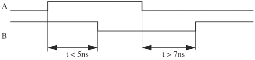
An example of a timing requirement is that a transition, triggered by other transitions, must occur within a time interval. In Figure 4.14, in_a, in_b, and out are the inputs and output of a design that requires that signal out, triggered by both in_a and in_b, which are synchronized to clock, rise when both inputs fall. A timing specification for this rising transition is that the transition must occur between the second and the third clock rising edge. This is synchronous specification, because the timing requirement references a clock. An example of an asynchronous timing specification is that signal out falls when both inputs have risen, and must do so within the interval [2ns, 6ns].

The timing specifications among in_a, in_b, and out can be verified in the test bench. These timing requirements are examples of the generic specification form that mandates that a transition occur within an interval [t1, t2]. Checking transitions occurring in an interval can be done in two steps. The first step checks the lower limit, and the second step checks the upper limit—t1 ≤ t and t ≤ t2. If the transition is caused by a condition on a set of inputs (for example, both inputs are high), time is measured from when the condition is met to the time the transition occurs. The measured time is compared with t1 or t2. A condition bit is used to denote that a triggering condition is met. Let’s use the previous timing specifications for illustration and assume the time unit is 1ns. The first specification is that signal out rises in [2T, 3T], when both in_a and in_b become low. The second specification is that out falls in [2ns, 6ns], after both in_a and in_b become high.
The first specification is a synchronous specification and it is broken into two specifications: 2T ≤ t and t ≤ 3T. Because it is a synchronous timing specification, the clock is used to strobe the checking code. For example, the following code checks for early arrival of signal out, making sure that signal out will arrive at least two cycles after both inputs are low (2T ≤ t):
assign condition = in_a | in_b;

@(negedge condition)
begin
   if ( out == 1'b0 )
   begin // now start measuring time
      repeat (1)
        @ (posedge clock)
        if (out == 1'b1) $error ("violate lower time limit.");
   end
   else // out == 1'b1
      $error("violate lower time limit.");
end
Because signal condition is triggered by clock, the clock transition seen by the block is the second transition after the one that changes condition—in other words, repeat (1) instead of repeat (2).
Now, check the upper time limit, t ≤ 3 T:
@(negedge condition)
begin
   arrived = 1'b0;
   if ( out == 1'b0 )
   begin // start measuring time
      repeat (3)
        @ (posedge clock)
        if (out == 1'b1) arrived = 1'b1;
   end
   else
      // anomaly, out did not start with 0, error.

   if (arrived == 1'b0) error ("violate upper time limit");
end
This code checks for the arrival of signal out for every clock transition up to three. If it arrives, flag arrived is set. Here we assume that in_a and in_b cannot cause condition to have another rising transition before three cycles have passed. If this is violated, the block checking the upper limit would miss the second rising transition of condition.
For asynchronous timing specifications, there is no reference clock; therefore, real time is used. Checking the lower limit can be done by creating two processes when the condition bit rises: One watches for time and the other watches for the out transition. When the lower limit expires, it checks output for the required transition. If it has already arrived, the lower limit is violated. Sample Verilog code is as follows.
condition = in_a & in_b; // both inputs high => trigger
...
@ (posedge condition)
begin // start checking
  arrived = 1'b0;
  fork: check_lower_limit
     // delay T1 (2ns), the lower time limit

    #2 disable check_lower_limit;
    // record arrival of signal out
    @ (negedge out) arrived = 1b'1;
  join

  // error if out comes before lower time limit expires.
  if(arrived == 1b'1) error ("lower time limit is violated");
end
Checking the upper time limit is done similarly, as shown here:
condition = in_a & in_b; // both inputs low => trigger
...
@ (posedge condition) begin // start checking
  arrived = 1'b0;
  fork: check_upper_limit
     // delay T1 (6ns), the upper time limit

    #6 disable check_upper_limit;

    // record arrival of result signal
    @ (negedge out)
    begin
      arrived = 1b'1;
      disable check_upper_limit;
    end
  join

  // error if result is late.
  if (arrived != 1b'1) error ("upper time limit is violated");
end
Note that the fork process should be disabled on the arrival of signal out or when the upper time limit expires. In the check lower limit case, the fork process is disabled only when the lower time limit expires.
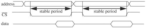
The previous discussion focuses on verifying timely transitions. The other side of the coin is to verify the absence of transitions in a time interval (in other words, stability of signals). An example of such a specification is that the address line of memory be stable until the ongoing write is completed. The idea is to use the event operator @ to detect transitions on the signals required to be stable until the enforcement period is over. This can be done by forking two processes, one detecting transitions and the other disabling the first process when the enforcement period expires. Using the memory example, assume that CS (chip select) is lowered when memory is accessed. Therefore, the enforcement period is the interval when CS is low (see Figure 4.15). Sample code verifying that the address is stable during an access cycle is as follows:
@(negedge CS) // CS is active low
begin
  fork: stable_address
    @(address[0] or address[1] or ... address[31])
      $error("address changes while accessing.");
    @(posedge CS) disable stable_address;
  join
end
Note that to detect changes in address bits, the bits must be spliced in the event operator, because @ (address) will only detect changes in the LSB of the address, per IEEE standard 1364-1995.
Every test bench uses utility routines common to other test benches. Therefore, for productivity, it is best to create a library of common facilities shared by most, if not all, test benches. This utility library can be included as a header file in a test bench. These utilities can take on the form of a module, a task, or a function. If it is designed as a module, it has to be instantiated when it is used. If it is designed as a task or a function, it must reside inside a generic module and must be accessed through a hierarchical path. The following code illustrates this idea. File utility.v is a library of utility routines and should be included when the utility routines are used. In this example, the test bench file uses two utility routines. The first is a module, util_dump_reg, and the second is a task, util_check_cache. To use the module routine, it instantiates the module. To use the utility task, the generic module containing it is instantiated. The task is then accessed through a hierarchical path:
// this file, utility.v, contains utility routines

// this routine takes the form of a module
module util_dump_reg (register, clock);
input register;
input clock;

always @(clock) $display("...", register);
...
endmodule

// this routine contains all utility tasks and functions
module util_generic_routines;
...
task util_check_cache(...);
begin
...
endtask
...
endmodule
// test bench file
'include utility.v

module top;
...
util_dump_reg util_mod (...); // call utility module by
  instantiation
...
util_generic_routines util_gen (...); // instantiate generic
  routines
...
top.util_gen.util_check_cache (...); // access utility task
  via hierarchical path
...
endmodule
Some commonly used verification utility routines are a random error generator and an injector, error and warning display routines, memory loading and dumping mechanisms, assertions of various kinds, routines that search patterns in memory, and other miscellaneous types. The list varies from project to project. Here we will study only a subset in detail.
An error injector generates pseudorandom errors and forces specified signals to take on the erroneous values. An error injector can be turned on or off. When it is off, it has no effect on the design. The purpose of an error injector is to verify that the design can gracefully detect errors, handle errors, recover from errors, or accomplish a combination thereof.
A block depicting a general-purpose error injector is shown in Figure 4.16. The error injector has a switch to turn error injection on or off. If turned off, its output is directly connected to the input without any error injected. If turned on, it modulates the incoming signal with a random or a hard-coded error. The resulting output can have a varying degree of impairment. One extreme is an output that is independent of the original signal and is simply the output of a random number generator. This models the situation when the original signal is totally disconnected and the receiver picks up noise. The other side of the impairment spectrum consists of modulation of the original signal by an error of varying degree of severity. Error modulation can be implemented in many ways. One way is to add a random number to the input signal; another is to invert certain bits of the input.
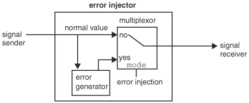
The following module is an implementation of an error injector of additive noise:
module error_injector (in, mode, out);
input [31:0] in;
input mode;
output [31:0] out;

reg [31:0] error;

  always @(in[31] or ... or in[0])
    error = $random;

  assign out = (mode == 1'b1) ? out = in + error : out = in ;

endmodule
When an error or a warning is encountered, two decisions need to be made. The first one decides the amount of information to be displayed (or dumped) about the error or warning. The second decision determines the course of the simulation: continue, stop, or pause for user direction. Both decisions are a function of the severity or priority of the error or warning. Therefore, a well-developed error and warning alert mechanism shows the type of error or warning it encounters, the scope in which it occurs, and has the capability to ignore certain types of errors or warnings and to halt the simulation if a serious error is encountered. Such a mechanism can be implemented as a user PLI task or a Verilog task. A sample user PLI task interface is
$alert (type, severity, action, message);
where type indicates whether it is an ERROR or a WARNING; severity classifies the type of error or warning as HIGH, MEDIAN, or LOW; action can be HALT the simulation or IGNORE the error or warning; and message is any user-specified text output. A sample use is as follows:
if ( toggle == 32'hDEAD )
  $alert (ERROR, HIGH, HALT, "unexpected dead signal. Inputs
are: sig_1=%h, sig_2=%h,...", sig_1, sig_2, ...);
And the result is halting the simulation with an output message like
At time 23292: ERROR (high priority, simulation stopped):
  In module top.design...arb, unexpected dead signal.
  Inputs are: sig_1=32'h024ad, ...
The time stamp and the scope are built into the task and show the time the error or warning was encountered and the scope in which the erroneous signal resides. Other arguments in an error and warning task are possible, such as arguments to specify dump filename and dump format if the error or warning warrants signal tracing.
Loading memory involves opening a file, reading the data, and writing the data to memory. A memory loader is used frequently during verification. For example, during initialization, a compiled image is loaded into the design’s instruction memory, or at the end of a simulation, data memory is dumped out for examination. Thus, a memory loading and dumping mechanism should be included in a verification utility library.
Such a memory mechanism can be implemented using Verilog constructs or C/C++ construction. The former is simpler and its basic operation is the Verilog system task $readmemh and $readmemb, which take a filename and memory, and store the data in the file to memory. For example, the following statement transfers data in file image to memory mem:
// declaration of a 1K 32-bit wide memory
reg [31:0] mem [1023:0];

// transfer data in file image to memory mem
$readmemh ("image", mem, START_ADDR, END_ADDR);
The first argument is the filename, the second is memory, the third is the starting address, and the fourth is the last address to be written. System task $readmemh assumes the data are in hex, and $readmemb assumes the data are binary.
A better equipped memory loading and dumping mechanism issues warnings when anomalies are encountered, such as cannot open a file, memory argument not declared as memory, amount of data overflows the specified address range, or starting and ending addresses fall out of the range declared. To have this feature, the memory loader is usually implemented as a user PLI task instead of a Verilog task, because memory cannot be passed to a Verilog task. However, memory can be passed to a user PLI task, with the PLI task argument being a “word select” of the memory. However, the entire memory can be retrieved using PLI function tf_nodeinfo(), regardless of the word select. Once the memory is on hand inside the C/C++ code, it can be read or modified. The following call to a user PLI task illustrates passing memory mem to user PLI task $util_memory_loader, where word select 0, mem[0], is arbitrary as long as it is within the declared range:
// passing memory to user PLI task
$util_memory_loader ("file_name", mem[0],...);
Even though only the first word of mem was passed to $util_memory_loader, all memory can be accessed in the C/C++ code through the PLI function tf_nodeinfo(). As an example, suppose the following C code implements $util_memory_loader():
void util_memory_loader()
{
  s_tfnodeinfo nodeInfo;
  char *first_address;

  tf_nodeinfo(2, &nodeInfo);
  first_address = nodeInfo.node_value.memoryval_p;
  ...
}
The Verilog memory mem is accessed using tf_nodeinfo(2, &nodeInfo), the first argument of which is the argument number in the user PLI task call. In this case, it is 2 and it points to mem[0]. Data in memory mem are then stored in nodeInfo, which points to a data structure:
struct t_tfnodeinfo
{
  ...
  union {
    ...
    char *memoryval_p;
    ...
    } node_value;
  int node_ngroups;
  int node_vec_size;
  int node_mem_size;
} s_tfnodeinfo;
where node_value.memoryval_p points to the start of the memory array, node_mem_size contains the number of words in the Verilog memory, node_vec_size is the width of a word, and node_ngroups is the number of groups in a word. A group is an 8-bit byte of a Verilog memory word; thus, a 32-bit word has four groups. The concept of a group becomes clearer when the mapping from Verilog memory array to C array is illustrated.
A Verilog memory array is mapped to a C array in PLI. Each word is represented by a C array of characters. A word, which can be of any length, is partitioned into groups of 8 bits. Each group is represented by a C character. For example, a word of 32 bits is represented by four groups. The groups for a word form an element in the C array. Therefore, the number of words in Verilog memory is equal to the number of elements in the C array.
In Verilog, a bit range can be declared in decreasing or increasing order, such as reg [31:0] mem [...] or reg [0:31] mem [...] respectively. In decreasing order, bites 7, 6, ...,0 form the LSB, whereas in increasing order bytes 24, 25, ..., 31 form the LSB. Bytes in a Verilog word are represented by groups in a C element. The mapping between the bytes and the groups is that the LSB is always mapped to group 0. Figure 4.17 shows the mapping. Note that the bit order within a byte and a group is preserved.

Similarly, Verilog memory’s word range can be declared in decreasing or increasing order, such as reg [...] mem [1023:0] and reg [...] mem [0:1023] respectively. However, address 0 is always mapped to C_array[0], and so on, as shown in Figure 4.17.
In four-state representation, two bits (a,b), are used to represent the four possible values 0,1,X, and Z. The 2-bit patterns are (0,0) for 0, (1,0) for 1, (0,1) for Z, and (1,1) for X. The two bits are called aval and bval. So, for every byte in Verilog, two groups are required in C. A 32-bit word thus requires eight groups in C to be represented. The mapping of the bytes and the groups is shown in Figure 4.18.
With mapping understood, a location at address N in Verilog memory can be accessed in C using the following indices. aval and bval are obtained separately, and their bits are combined to get the four-state value:
char *avalp; // pointer to aval
char *bvalp; // pointer to bval
char *base_addr; // the starting address of the memory
int word_size; // word size in C
int ngroups; // number of groups
base_addr = nodeInfo.node_value.memoryval_p;
ngroups = nodeInfo.node_ngroups;
word_size = ngroups * 2; // 2 comes from aval and bval
avalp = base_addr + N * word_size;
bvalp = avalp + ngroups;
For example, if the first bytes of aval and bval are 10100000 and 11000000 respectively, then the four-state value of the first byte is XZ100000. Using the previous indices, Verilog memory can be read or written to any value.
A memory dumping mechanism can be similarly constructed. The basic Verilog system tasks are $dumpmemh and $dumpmemb. A user system task can provide checks for valid address range, file permission, and a format conversion facility. Again, passing in memory can be achieved through a PLI argument using tf_nodeinfo(). An example memory dumping facility interface is as follows:
if(dump_flag) // a typical usage
  $util_memory_dump("file_name", memory[0], start_address,
end_address, format);
When a design has a lot of on-chip memory or is simulated with large off-chip memory, this memory is called design memory and often it is not fully used during verification. For instance, a CPU may have hundreds of megabytes of memory, but data and instructions in a simulation occupy only a small portion. To save memory, a simulator needs to allocate only simulation memory space equal to the amount actually used, and to use a dynamic table to map the occupied design memory locations to the simulation memory. This technique is called sparse memory modeling. The dynamic table mapping from design memory address space to simulator memory address space can be implemented with CAM, with an address that is a simulation address and with data in a design address (see Figure 4.19).
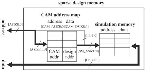
When a location in design memory is accessed, the upper bits of the address, [ASIZE:LB], are sent to the CAM address map to look up the corresponding CAM address. That part of the design memory address is compared with the contents of CAM. If it is found, the CAM address is returned and concatenated with the remaining lower bits of the design address, [LB-1:0], to access simulation memory. If it is not found, an entry is added to the CAM address map if it is not yet full. The new entry in the map contains the upper bits of the design memory address as the data and the corresponding CAM address as the address. If the CAM address map is full, it can be augmented or fewer upper bits of the design address are used in the map or the simulation memory is expanded. Using this sparse memory technique, the size of the simulation memory shadows the amount of design memory actually used, which is often a small percentage of the entire design memory. The following code illustrates a sparse memory implementation:
// ASIZE := design address size
// DSIZE := design data width
// SM_ASIZE := address of simulation memory
// LB := lower bits for CAM
// CAM_ASIZE := CAM address size, CAM_ASIZE = SM_ASIZE - LB
// CAM_DSIZE := CAM data size, CAM_DSIZE = ASIZE - LB

module sparse_memory (address, data, mode, cs);
input ['ASIZE:0] address;
inout ['DSIZE:0] data;
input mode;
input cs;

reg ['DSIZE:0] simulation_memory ['SM_ASIZE:0];
reg ['SM_ASIZE:0] sim_address;
reg ['DSIZE:0] mem_out; // simulation memory output

reg ['CAM_DSIZE:0] CA_memory ['CAM_ASIZE:0];
reg ['CAM_ASIZE:0] cam_address;
reg ['CAM_ASIZE:0] last_CAM_address; // pointer to last CAM
                                  // address
reg  found; // 1 = found entry in look-up table
reg add_ok; // 1 = successfully added an entry to look-up table

initial
begin
  last_CAM_address = ('CAM_ASIZE+1) 'b0;
end

always @(negedge cs)
begin
  // get simulation address for design address
  CAM_lookup (address ['ASIZE: 'LB], cam_address, found);
  // task modeling a CAM
  if( found != 1'b1)
  begin // add entry to look-up table
    CAM_add (address ['ASIZE: 'LB], cam_address, add_ok);
    if (add_ok != 1'b1) $error ("CAM full");
  end

  // form address to access sparse memory address
  sim_address = {cam_address, address ['LB-1:0]};
  if (mode == 'WRITE)
    simulation_memory[sim_address] = data;
  else if (mode == 'READ)
    mem_out = simulation_memory[sim_address];
  else
    $error("unknown mode");

  end // end of always

assign data = (mode == 'READ) ? mem_out : {('DSIZE+1) {1'bz}};

// task modeling CAM
task CAM_lookup;
input ['CAM_DSIZE:0] address_s; // shortened design address
output ['CAM_ASIZE:0] cam_address;
output found;

begin: cam_block
reg ['CAM_ASIZE:0] i;

found = 1'b0;
for (i=0; i≤=last_CAM_address; i=i+1)
begin
  if(address_s == CA_memory[i])
  begin
    found = 1'b1;
    cam_address = i;
    disable cam_block;
  end
end // end of for
end // end of named block
endtask

// add an entry to the look-up table
task CAM_add;
input ['CAM_DSIZE:0] address_s;
output ['CAM_ASIZE:0] cam_address;
output status; // 1 = ok

begin: cam_add_block
  // check whether CAM is full
  if(last_CAM_address == {('CAM_ASIZE+1) {1'b1}}) // CAM full
  begin
      status = 1'b0;
      disable cam_add_block;
  end
  else // CAM not full
      // add the address to the look-up table
      // return the next available simulation address
      status = 1'b1;
      cam_address = last_CAM_address;
      last_CAM_address = last_CAM_address + 'CAM_ASIZE'b1;
      CA_memory[cam_address] = address_s; // add entry
end
endtask

endmodule
Task CAM_lookup takes in an address and compares it with every stored entry in CAM—from 0 to last_CAM_address. If found, the corresponding CAM address is returned and the task is disabled. Task CAM_add checks whether the CAM address map is full by comparing the size of CAM with last_CAM_address. If it is not full, last_CAM_address becomes the CAM address of the incoming address, which is then stored as data in the new entry.
The value of LB has the following effects on the CAM address map and simulation memory. If it is too small, the address map becomes large. In the extreme when LB equals zero, every design memory address is stored in the address map; hence, the size of the address map is the same as the simulation memory. If it is too big, the simulation memory becomes large, approaching the size of design memory, and thus has many unused locations. In the extreme when LB equals the design memory address, all design address bits become the simulation memory address bits; meaning, the simulation memory is identical to the design memory. An example of storing data in sparse memory is shown in Figure 4.20, in which the value of LB was chosen to be 2. The upper 3 bits of address 101001, 101, are mapped to 0, which combines with the lower 2 bits 01 to form an address for the simulation memory: 001. The data, 11010, are then stored at 001 in simulation memory. Design memory uses a 5-bit address, but simulation memory uses only a 3-bit address.
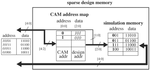
Verification utility can also include assertions. Assertions compare signals with their expected values on the fly and issue warnings or errors when they do not match. There are some common assertions that should be standardized within a project and should be grouped in a verification utility library. The set of such assertions varies from project to project. These assertions can be implemented either as Verilog tasks or user PLI tasks. For an in-depth study on assertion, please refer to “Assertions” on page 232.
The interface mechanism between the test bench and the design under verification is responsible for exchanging data between them and can be a combination of the following methods: design I/O ports, hierarchical access, file I/O, and PLI. Using the design’s I/O ports to pass data between the design and the test bench is usually reserved for signals to which the design would physically connect in an application—for example, data and address lines of a microprocessor. Observation signals for verification purposes (such as internal registers or nodes) are accessed through hierarchical paths, because to read an internal register through the design’s I/O ports could require an elaborate and long control sequence. In contrast, hierarchical accesses can read or write to the nodes or registers immediately. However, hierarchical accesses must not be used among nodes inside the design, because a hierarchical access cannot be implemented physically.
The design and its test bench can also exchange data through file I/O. The design prints signal values to a file, which is then read by the test bench for analysis, or the test bench writes stimuli to a file to be read by the design. File I/O is slow and is usually used for one-time I/O (for example, loading stimuli at the start of a simulation or dumping out node values at the end of a simulation). An advantage of file I/O is that analysis can be done after the simulation is finished, so it is used when simulator time is scarce (such as with a hardware simulator) or when the analysis time is long.
The design can also have an interface with a test bench through PLI. In this case, the interface on the Verilog side is a user-defined system task. Whenever the user task is encountered during simulation, the control is transferred to the C program implementing the task. Using PLI can be slow, especially for a hardware simulator, in which the simulator stops and transfers control to the host machine to execute the C program. On the other hand, when test bench computation is extensive and difficult to implement in Verilog, PLI is the preferred interface. Examples of a test bench using PLI are reference model verification and memory initialization. With reference model verification, a model of the design is implemented in C and is run in lock step with the Verilog code of the design. At the end of each cycle, registers in Verilog are compared with the corresponding ones in the C model. Memory initialization loads the object codes for the design into the Verilog model of the data and instruction memory of the design. The loader is implemented using PLI. Figure 4.21 illustrates and summarizes various interfaces.

Making a test bench or a verification environment work for a design is the first step toward the ultimate goal: building on the working environment and creating a verification infrastructure that is easily adaptable for future designs. In this section, we look at several common techniques and methodologies that further this goal. The general principle is to hide implementation details and raise the verification infrastructure to a level where people can operate and maintain it with simple and meaningful procedures. Some such practices include centralizing configuration parameters and encapsulating low-level operations with high-level procedures.
A configuration is a particular combination of certain representations and/or components in the design and test bench. For example, a design can have a gate-level as well as an RTL representation, a design can have a representation in which all scan chains are connected or disconnected, or a verification setup can have all assertions turned on or off. An example of a configuration, a combination of these representations, is a circuit in RTL with all scan chains disconnected and all assertions turned on. A configuration can be regarded as a view of the design. An RTL configuration is a view of the design at the RTL, whereas a gate-level configuration is another view of the same design. Similarly, the same design can also have a synthesis view and a verification view, among many other possibilities. Multiple configurations, or views, can be embedded in a single set of design files using ifdef directives. A pictorial illustration of embedding multiple views in a single set of files is shown in Figure 4.22. In the figure, there are three views: a gate-level view, an RTL view, and a verification view. The gate-level and the RTL views describe the same functionality—an adder. The verification view has the verification codes for the adder. All these views can be embedded in the same file.

Directives 'ifdef, 'else and 'endif form the delimiters to include or exclude code to be compiled. An example use is
'ifdef X
  code_A
'else
  code_B
'endif
If variable X is defined, using define X in Verilog or +define+X on the command line, code_A is included and compiled, and code_B is omitted. If variable X is not defined, code_B is included instead. Directive 'else is optional. Therefore, a configuration is just a collection of variable definitions. For instance, to include the RTL and the verification views of the adder in Figure 4.22, simply do the following in Verilog:
'define RTL
'define VERIFY
or, on a command line of a Verilog compiler, do this:
verilogCompile -f filelist +define+RTL+define+VERIFY ...
The following example shows two ifdef's embedding four possible configurations:
SYNTHESIS and VERIFY, NOT SYNTHESIS and VERIFY, SYNTHESIS and NOT VERIFY, and NOT SYNTHESIS and NOT VERIFY:
'ifdef SYNTHESIS
  RTL codes A ...
'else
  RTL codes B ...
  'ifdef VERIFY
    RTL codes C ...
  'else
    RTL codes D ...
  'endif // VERIFY
  RTL codes E
'endif // SYNTHESIS
A configuration can also change component settings by using macro-defined directives. For example, in the following code, macro PERIOD takes on any value in the range 1, ..., 8, and thus PERIOD alone generates eight possible configurations:
// define macro PERIOD to have value 7
'define PERIOD 7
$Generate_clock(PERIOD, ...);
To select a particular configuration, the corresponding variables or macros are defined (for example, 'define PERIOD 7).
To make the design and test bench easy to maintain, all defines and definitions should be centralized to the configuration file. Outside the configuration file, there should not be any variable defines or macro definitions. The configuration file is included as a header whenever necessary. A sample configuration file, config.v, may look like
// system configurations
// defines
'define VERIFY
'define SCAN
...
// macro definitions
'define SEED 7
'define ITER 100
...
Besides defining variables and macros in a header file, they can also be defined on the command line. For example,
compile filelist +define+VERIFY + define+SCAN + define+SEED=7
+define+ITER=100 ...
In this case, the configuration file can be an input to a make utility, which generates the compile command with the correct configuration. Again, the purpose of having a centralized configuration file is to eliminate passing to a verification environment multiple conflicting configurations or missing configurations.
As the name implies, a bus functional model encapsulates detailed operations among the test bench and devices under verification as high-level procedures that resemble commands a device receives from or sends to the bus. To exercise a device, high-level bus instructions, instead of bit patterns, are issued. The instructions are translated into low-level bits and are applied to the device by predefined procedures. So, interactions among the test bench and the devices are done at the transaction level. To have a bus functional model for a device is to create a wrapper that enables the device to receive and send bus commands, and the wrapper disassembles and assembles the commands into bits. The wrapper is sometimes called an interpreter or a transactor. The main advantage of using a bus functional model or a transaction-based model is that people only deal with high-level meaningful instructions, making the verification environment easy to maintain and adapt, and less prone to errors. Figure 4.23 shows the components and structure of a bus functional model in a verification environment. The figure has two devices under verification: a CPU and memory. Each device has its own command set. In this example, for simplicity, each device is assumed to have three commands: read, write, and status. For each command, there is a corresponding transactor that translates the command into bit vectors required for the device to perform the command. For example, a READ command calls the read transactor, which generates bit patterns for read and passes to the device. The set of transactors for a device is the device’s interpreter or bus functional model wrapper. The test program consists of high-level commands, also called transactions, and sends them to the bus functional model of the devices.
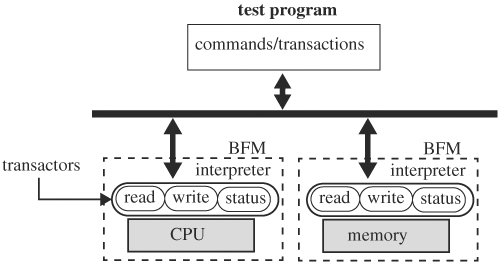
To make the concept more concrete, let’s construct a bus functional model for memory. Let memory have the simplified read and write timing diagrams shown in Figure 4.24.
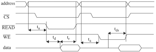
To read, signal READ must be ta after the address is stable, and READ must persists for tr so that the output data are stable. Data will be available for reading after td. To write, signal WE must wait for ta after the address is stable, and WE must hold for tds after the data are stable.
The following code illustrates a test bench that instantiates memory, defines two tasks (one for read and the other for write), and uses the tasks to test the memory. Let’s use parameters to represent the timing constraints. This code structure is a standard verification setup but is not a bus functional model:
module testbench;
//memory instance
memory mem (.CS(CS), .read(READ), .WE(WE), .address(address),
.data(data));

// read from memory
task read_memory;
input [31:0] in_address;
output [63:0] out_data;
begin
  address <= in_address;
  CS <=1'b0;
  #'ta READ <= 1'b0;
  #'td out_data <= data;
  # 'tr READ <= 1'b1;
  CS <= 1'b1;
end
endtask

// write to memory
task write_memory;
input [31:0] in_address;
input [63:0] in_data;
begin
  address <= in_address;
  CS <=1'b0;
  #'ta WE <= 1'b0;
  data <= in_data;
  #'tds WE <= 1'b1;
  CS <= 1'b1;
end
endtask
// test bench code testing the memory
always @(posedge clock)
begin
  write_memory(addr1, data1);
  @(posedge clock)
  write_memory(addr2, data2);
  ...
  @(posedge clock)
  read_memory(addr1, result1);
  ...
end

endmodule // test bench
A bus functional model groups the design and its associated tasks as a module so that operations on the resulting module, BFM, are performed by calling the module’s tasks. Translating this code into memory BFM, we have
module memory_BFM (address, data);
input [31:0] address;
inout [31:0] data;

  memory mem (.CS(CS),.read(READ),.WE(WE),
.address(address),.data(data)); // memory instance

  task read_memory;
    ...
  endtask

  task write_memory;
    ...
  endtask
endmodule // memory_BFM

module testbench;
  memory_BFM mem(.address(addr),.data(data));

  always @(posedge clock)
  begin
    mem.write_memory(addr, data);
    @(posedge clock)
    mem.write_memory(addr, data);
    ...
    @(posedge clock)
    mem.read(addr, data);
  end
endmodule // test bench
Note that the bus functional model now has only two arguments: address and data. Signals CS and WE are no longer visible. This is reasonable because address and data are transaction-level entities whereas CS and WE are signaling entities that the user should not be concerned with. Of course, if the user intends to verify the signaling correctness of all interface signals, CS and WE need to be specified in the model.
At first glance, the difference between this bus functional model and the standard test bench seems to be quite trivial. This difference becomes significant when there is more than one component under verification. In this case, if the bus functional model is used, each component has its own encapsulated operational tasks. All operations in the test bench are done at the transaction level by simply calling the device’s task. An example test bench with multiple devices may look like
module testbench;
// device instances
device1 dev1 (...);
device2 dev2 (...);
device3 dev3 (...);

// transactions among devices
@(posedge clock)
dev1.op1 (...);
dev2.op1 (...);
dev3.op1 (...);
...
@(posedge clock)
dev1.op3 (...);
dev2.op5 (...);
dev3.op2 (..);
...
endmodule // test bench
Try to use the standard test bench structure to set up the previous multiple-device environment. You will notice the confusion among the operations for the devices. If two devices have the same operation (for example, READ), you will have to use different names for the tasks. Furthermore, the tasks are not grouped with their design and hence are more difficult to maintain.
In this chapter we studied the major components of a test bench: initialization, clock generation and synchronization, stimulus generation, response assessment, test bench-to-design interface, and verification utility. For initialization we looked at initialization using RTL code and PLI routines, with predetermined and random values. For clock generation and synchronization we presented several methods to produce clock waveforms. We also discussed the effect of time scale and resolution. We then examined the synchronization of different clock domains. For stimulus generation we presented synchronous vector application, asynchronous stimulus application, and instruction code stimuli. For response assessment we considered assessment methods using waveform tracing, monitors, golden files, and self-checking routines. Besides functional assessment, we presented methods to monitor timing constraints. We examined four types of test bench and design interface mechanisms: I/O ports, hierarchical paths, PLIs, and file I/O. As noted, verification utility routines are often-used routines and are created to increase productivity. The set of such routines varies from project to project. In this chapter we discussed methods for error injection, memory loading and dumping, sparse memory modeling, and some widely used assertions.
We examined some common methodologies and practices. In particular, we discussed test bench configuration and the bus functional model. Test bench configuration embeds several views of the same RTL code in the same file. A view can be invoked by defining a particular variable. The bus functional model encapsulates detailed operations into high-level transactions. We discussed how a design and its operational commands are packaged to form a bus functional model, and how the bus functional model can be used in a test bench.
1. | Write a test bench that initializes the following FF output to value module flip=flop (Q, D, clock); output Q; input D; input clock; always @(posedge clock) Q <= D; endmodule // end flip-flop module testbench; // initialization codes here ... flip_flop ff(.Q(q), .D(d), .clock(clk)); endmodule // test bench |
2. | Initialize the following latch, driven by the clock, to module latch (Q, D, clock);
...
always @(clock or D)
if(clock == 1'b1)
Q <= D;
endmodule // end of latch
module testbench;
initial
clock = 1'b1;
always #1 clock = ~clock;
latch gate(.Q(q), .D(d), .clock(clk)); //
endmodule // end of test bench
|
3. | Initialize memory
|
4. | Initialize the memory in the previous problem to random values. |
5. | Write a PLI routine to initialize memory with data from a file. (This problem is for those who know how to write PLI functions.) |
6. | Write Verilog code to generate the waveforms presented in Figure 4.25. |
7. | The following clock starts at high. The transition to high at time zero may be considered a legitimate transition for some simulators but may be ignored by others. Write Verilog code to determine whether your simulator ignores time zero transition. |
8. | What clock periods do you expect to see when the following code is simulated?
|
9. | Write Verilog code to generate the clock waveform shown in Figure 4.26, where the falling and rising transitions have 300ps and 200ps jitter respectively. In other words, the edges transit randomly with an uncertainty of 300ps on rising and 200ps on falling. |
10. | Compile the following C code. Call the resulting binary file main () {
int x, y, z;
x = 12;
y = 21;
z = x + y;
}
|
11. | Write RTL code to dump out variables within a module of your choice using
|
12. | In this problem, calculate the cost in maintaining golden files. Assume that 10% of RTL changes require updating the golden files and there are ten RTL changes per day. For each golden file update, the design is simulated over 100 diagnostics, each of which takes ten minutes.
|
13. | Self-checking code can be executed through RTL or a PLI. For the following design, write a self checking test bench. You need to decide whether it should be in RTL or PLI.
|
14. | Write tasks to detect the timing violations in the waveforms shown in Figure 4.27. |
15. | A communication device receives an incoming clock up to M Hz. Write a task to enforce this maximum frequency requirement. It should issue an error if the input frequency exceeds M Hz. |
16. | Write an error injector for the following memory model. The injector selects a random address and writes a random data to the address at rising transition of a global signal module memory (ReadWrite, CS, address, data); input ReadWrite; // 1=read, 0=write input CS; // 0 = select input [31:0] address; inout [31:0] data; ... endmodule |