Once a design is free of statically detectable errors, it is ready to be verified by simulation. To use a simulator effectively, it is imperative first to understand its architecture. Following this philosophy, this chapter is organized in two parts: The first part is devoted to architectures of simulators, and the second discusses simulator operations. In studying simulator architecture, we will examine in depth two typical simulators on the extremes of the simulator spectrum. We then discuss how simulator types in the middle portion of the spectrum can be constructed, followed by a comparative study of the various types. In the second part of the chapter, common and advanced features of simulators are presented along with their applications.
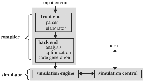
Generally, a simulator consists of three major components: a front end, a back end, and a simulation engine/control, as shown in Figure 3.1. The front end is very much standard for most simulators and is a function only of the input language. The back end performs analysis, optimization, and generation of code to simulate the input circuit, and is the main contributor to a simulator’s speed. The front end and the back end form the compiler portion of a simulation system. The simulation engine takes in the generated code and computes the behavior accordingly. In this stage, the generated code has no direct knowledge of the circuit and can be in any language. If the generated code is C/C++, it first needs to be compiled using a C/C++ compiler before it is run. If the generated code is the native code of the target machine, it can be run immediately. Simulation control allows the user to interact with the operation of the simulator. An example of user control is to run a simulation in interactive mode, as in debugging a design, in which the user can set break points to pause a simulation after a number of time steps, examine variable values, and continue simulation.
The front-end portion of a compiler, consisting of a parser and an elaborator, processes the input circuit and builds an internal representation of the circuit. Specifically, a parser interprets the input according to the language’s grammar and creates corresponding internal components to be used by the elaborator. For example, a module is parsed into an internal programming object that has fields for the module name, port name, port type, and a link list of all entities inside the module. The elaborator constructs a representation of the input circuit by connecting the internal components, substituting parameters, inlining or setting up parameter passing for functions and tasks, and others. For instance, the elaborator substitutes a module instantiation with the module’s definition and connects the internal objects consistent with the circuit connectivity. Sometimes the elaborator applies optimization to the internal representation. The end result from an elaborator is a complete description of the input circuit sufficient to sustain all later processing and operations.
The back end, the soul of a simulator, determines the type of the simulator. The actual operations of the analysis stage vary from one type of simulator to another. For a cycle-based simulator, it performs clock domain analysis and levelization, whereas for an FPGA-based hardware simulator, in addition to the previous analysis it also partitions, places, and routes the circuit into FPGA chips. For this reason, an in-depth discussion of analytical stage is relegated to the sections on specific simulators.
The type of simulator also dictates the construction of code generation. There are four classes of generated code: interpreted code, high-level code, native code, and emulation code. The last three are sometimes referred to as compiled code.
In an interpreted simulator, the input circuit is compiled into an intermediate language for the interpreted simulator. The interpreted simulator can be regarded as a virtual machine that reads in instructions in the intermediate language, one instruction at a time. The effect of executing the interpreted object code creates the behavior of the circuit. The diagram in Figure 3.2 depicts this interpreted simulation process. The interpreted simulator is a virtual machine with the interpreted code as its instructions. The instructions are fetched, one by one, then are decoded and executed. The interpreted simulator has a user interface to allow data examination and execution control. An example of interpreted code and the circuit it simulates is as follows:
      // circuit being simulated
      initial
      begin
      clk = 1'b0;
      #1 clk = ~clk;
      #1 clk = ~clk;
      #1 finish;
      end

      always @(clk)
      begin
         a = b & c;
         if (a == 1'b0)
            p = q << 3;
      end

      // generated interpreted code
      assign(clk, 0);
      invert(clk);
      evaluate(b1);
      invert(clk);
      evaluate(b1);
      exit();

      b1: //definition of routine b1
      {
         and(a,b,c);
         if(a,0) left_shift(p,q,3);
      }

The functions in the interpreted code—assign(), invert(), evaluate() —are instructions for the interpreted simulator. Note that the stimulus or test bench is compiled with the circuit.
Interpreted code is very portable. Compiled once, the code can run on any machine that has an interpreted simulator. However, its simulation is the slowest compared with the other three kinds, because of the extra layer of execution on top of the native machine.
A compiler can also compile a circuit into a high-level language such as C/C++. To simulate, the generated C/C++ description of the circuit is compiled with a C/C++ compiler and is run just like any other C/C++ program. A sample generated C program simulating the previous circuit is shown here. By analyzing the Verilog code, it is determined that the clock toggling statement can be combined with the always block. In general, such a simplification may not exist. In that case, the C code of the always block will have to be run on a separate thread that constantly monitors changes in the clock variable. A change on clk will trigger an evaluation of the C code representing the always block:
      main()
      {
         int clk;
         int i;
         int a, b, c, p, q;
         clk = 0;
         for (i=0; i<2; i++) {
            clk = (clk == 0) ? 1 : 0 ; // clk = ~clk;
            a = b & c; // always block
            if (a==0)
               p = q << 3;
      }
High-level code is not as portable as interpreted code because high-level code needs to be recompiled to the native language of the platform (for example, SUN workstations) every time it is simulated. This compile time can be long because the high-level code is usually very large. High-level code is portable to a certain degree, because the generated high-level code compiled from the circuit can be reused.
Native code compilation, skipping the intermediate language generation step (for example, C/C++ or interpreted code), directly produces the machine executable code for the platform. At the expense of portability, native code runs slightly faster than high-level code because of the more direct machine code optimizations. Both native code and high-level code are typically about 5 to 20 times faster than interpreted code. The major shortcoming for native code compilation is portability.
Finally, in hardware simulators/emulators/accelerators, the compiler generates the machine code for the hardware simulators/emulators. During simulation, a hardware simulator sometimes requires interaction with the host machine. An example of such an interaction is running C code in the host simultaneously with the circuit simulation in the hardware simulator (for example, PLI C code running on the host in lock step to compare result with that from the hardware simulator at the end of each cycle). (This is discussed further, later in the chapter.) This type of interaction is a major bottleneck in simulation performance. If the host-hardware interaction can be minimized, simulations on hardware are orders of magnitude faster than those in software simulators, typically in the range from 100 to 10,000 times. The disadvantages are long compilation time and capacity limitation (the maximum size of the circuit that can fit into the simulator). Figure 3.3 summarizes the four types of simulators and their simulation processes.

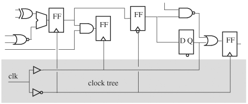
An interpreted simulation system has a clear separation between code of the compiled circuit and code of the simulator, with the circuit code feeding the simulator, as indicated in Figure 3.2. However, a compiled simulation system is composed of a single piece of compiled code that combines the circuit, the simulator, and a user interface program. The structure and execution flow of a compiled simulator is shown in Figure 3.4. The compiled code, the output of the compiler, has instruction memory that represents the circuit connectivity and its components’ functionality, data memory that stores simulation values of nodes and variables in the circuit, and a simulation engine, sometimes called a simulation kernel, that manages scheduling, controls component evaluation, stores and retrieves simulation values, advances time, handles exceptions and interrupts, distributes tasks to processors in the case of a simulation using multiple processors, and other duties. To illustrate the simulation structure, consider a transition occurring at the primary input of a gate-level circuit. The simulation engine determines the fanin gates affected by the transition by following the connections of the primary input in the instruction memory, and places fanout gates in an evaluation queue. For each component in the queue, the evaluation starts by looking up its functionality in instruction memory and ends by storing the output values in data memory. When all events have been evaluated, the simulation engine advances the time.

The simulation engine and the simulation control unit form the simulator, but the engine resides inside the compiled code, and the simulation control unit lies in a separate program. If high-level code is generated, the object code of the simulation engine is linked with the object code of the compiled circuit to produce a combined object code. If native code is generated, the final result is the executable. In running a simulation, the control unit is invoked first, then the compiled code is loaded. Through the control unit, the user directs the simulation—for example, specify the time steps a simulation is to be run, setting break points, inspecting node values, dumping out signal traces, and check-point. An example of a compiled simulator is presented in “Cycle-Based Simulators” on page 88.
Many architectures of simulators exist. In this section we first study two contrasting architectures: event driven and cycle based. Through this discussion, we introduce various concepts, terminologies, and techniques, and their benefits and shortcomings. Then we move on to an investigation of hybrid and hardware simulators.
An event-driven simulator, as the name implies, evaluates a component, whether it is a gate or a block of code, only when there is an event at an input or sensitivity list of the component. An event is a change of value in a variable or a signal. If an event at a gate input causes one of its outputs to change, all the fanouts of the gate will have to be evaluated. This event ripples throughout the circuit until it causes no more events, at which time evaluation stops.
When multiple events occur simultaneously, each of which causes further events, the simulator, being able to evaluate only one at a time, must schedule an evaluation order of the events. Events are stored in an event manager, which sorts them according to event occurrence time. Events occurring at the same time are assumed to have an arbitrary order of occurrence. Evaluations are then executed on the stored events starting from the earliest time. When the simulator is at time T, all events that occurred before time T must have been evaluated.

In practice, the event queue is often implemented as a circular queue or a timing wheel, where the time queue wraps around itself, as shown in Figure 3.6. A timing wheel has time slots, and each time slot points to a queue that stores all events occurring at that time. Simulation progresses along the time slots. At each time slot, the events of the queue are evaluated one at a time until it is empty. During an event evaluation, if events are generated, they are inserted into the queue in the time slots at which they will occur. When all the events in the queue are examined, simulation advances to the next time slot.

Figure 3.6. A timing wheel: a two-dimensional queue made of a circular time queue and a linear event queue
The number of time slots in a timing wheel reflects an estimate of the maximum number of occurrences of future events, which is equal to the number of distinct delays from a primary input to a node. In practice, the size of the timing wheel is not equal to the maximum theoretical bound, but is equal to an empirical average. Therefore, it is possible that the timing wheel experiences overflow. When this happens, an overflow two-dimensional queue is created to hold the new entries. As simulation time advances, time slots on the timing wheel are freed so that new events can be placed there instead of in the overflow queue. An overflow queue is less efficient to manipulate than a timing wheel. Thus, choosing the right-size timing wheel has a palpable impact on simulation performance.
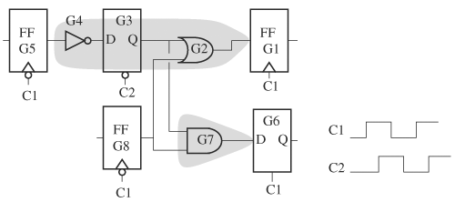
So far, we have assumed that all events in the same time slot are processed in an arbitrary order. However, events at the same time have to be prioritized according to IEEE Verilog standards. In Verilog, events at a simulation time are stratified into five layers of events in the following order of processing:
Active
Inactive
Nonblocking assign update
Monitor
Future events.
Active events at the same simulation time are processed in an arbitrary order. The processing of all the active events is called a simulation cycle. Inactive events are processed only after all active events have been processed. An example of an inactive event is an explicit zero-delay assignment (#0 x = y), which occurs at the current simulation time but is processed after all active events at the current simulation time have been processed. A nonblocking assignment executes in two steps. First it samples the values of the right-side variables. Then it updates the values to the left-side variables. A nonblocking assign update event is the updating step of a nonblocking assignment and it is executed only after both active and inactive events at the current simulation time have been processed. Note that the sampling step is an active event and thus is executed at the moment the nonblocking statement is encountered. Monitor events are generated by system tasks $monitor and $strobe, which are executed as the last events at the current simulation time to capture steady values of variables at the current simulation time. Finally, events that are to occur in the future are future events. Each time slot, in reality, points to four subqueues corresponding to the four groups of events. Within each subqueue, the order of events is arbitrary.
When an event is placed in a queue, it only means that the event may happen. Whether it actually will happen has to be evaluated. In the context of simulator design, events are further conceptually categorized into update events and evaluation events. An update event occurs when a variable or a node changes its value. When an update event has occurred, all processes sensitive to the variable or node are triggered and must be evaluated. This evaluation process is called an evaluation event. If an evaluation event of a process changes the values of some variables, then update events are generated for the affected variables. Therefore, an update event causes evaluations of the processes sensitive to it, which in turn may produce update events for their output variables.
The update event simply replaces the existing value of a variable or node with the new value. The evaluation event essentially simulates the gates or blocks sensitive to the update event. If the affected gates or blocks have no delays, the variables and nodes in the gates or blocks are computed at the current simulation time. If there are changes, update events are scheduled. If a gate or block has delays, then the result of the evaluation will be known only at a future time. When this happens, the evaluation schedules future events. These future events need to be validated at future times. It is possible that some of these scheduled future events may be canceled, as the following example demonstrates.
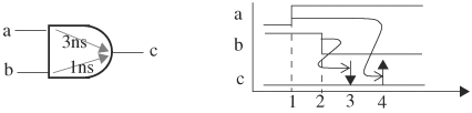
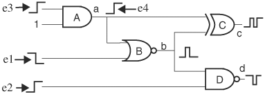
Figure 3.7. A predicated event is canceled because of a later event in a gate with asymmetric delays
Suppose that a future event is scheduled at time T. We now examine how the event is validated. At time T, the event is taken off the timing wheel. From the event’s content, we get the gate that was predicted to produce this event. Because all events up to the current time at all the inputs of the gate have already happened, all input waveforms are known up to the current simulation time. So we can compute the output transition at T, using the gate’s logic functionality and internal delay information. If a gate has internal delays, then only the portions of the input waveforms that are still “in flight” inside the gate need to be used. For instance, to compute the transition at the output of the AND gate in Figure 3.7, we only need to know the value at input a at time T - 3ns, and the value at input b at time T - 1ns. Input values at these times have just propagated to the output. In other words, only the portions of input waveforms determined by the gate delays, not the entire history, are required for validation. The computed output transition occurs if it is validated.
Let us illustrate this using the example in Figure 3.7. At time 1, the rising transition at input a schedules an event at time 4; and at time 2, the falling transition at input b schedules another event at time 3. Let us validate these two events. When the simulation advances to time 3, we first determine the values at the output that came from inputs a and b respectively. The value from input a is the value at input a at time 3 − 3 = 0. In other words, T minus the delay from input a to output c. The value at input a at time -1 is 0. The value propagating from input b is the value at input b at time 3 − 1 = 2, which is 0. (We compute a transition at the moment just after time T.) Therefore, the output is 0 at time 3. When the simulation advances to time 4, we validate the event predicted by the rising transition at input a back in time 1. The output value propagating from input a is the value at input a at time 4 − 3 = 1, which is 1. On the other hand, the output value from input b is the value at input b at time 4 − 1 = 3, which is 0. Therefore, the resulting output value at time 4 is 0. That is, the scheduled event at time 4 is canceled and the output remains 0.
This event validation algorithm is summarized in the following list. If the gate has multiple outputs, the outputs are validated one at a time:
When an event has been confirmed to happen, all fanout gates or blocks sensitive to the event must be examined for event propagation. At this stage, all fanouts should be assumed to propagate this event to their outputs and should be confirmed later at the event validation stage. It is dangerous to delete a future event at the current simulation time when it appears not to happen in the future. For example, an input of a 2-input AND gate goes high while the other one stays at 0 does not necessarily mean that the rising transition will not cause a rising transition at the output. A case in point is the AND gate in Figure 3.7 with input a rising, followed by b rising 1ns later. The b transition, although it arrives later, allows the transition from input a to propagate to the output.
A complicated component, with multiple paths from an input to an output, may produce more than one event at the output when it is triggered by a single input update event. In this case, all potential events must be scheduled. The time of occurrence of these potential events is then computed, and the events are inserted into the respective slots in the timing wheel.
Event propagation requires a knowledge of fanouts. It is interesting to note that fanouts can change during simulation. It is true that fanouts of a node never change during the simulation of a gate-level circuit. However, this is not true in an RTL simulation, and such code does occur in test benches. An example is the following block with two event operators @, assuming x is an output of gate A and y is an output of gate B:
gate A(.out(x) ,...);
gate B(.out(y) ,...);
always
begin
   @x
   a = b;
   @y
   b = c;
end
The block waits at @x for any event on x. So gate A has this block as a fanout. After an event from x has occurred, the block proceeds until it hits @y, where it waits for an event on y. Now gate A no longer has the block as a fanout. Instead, gate B has it as a fanout (the fanouts of gates A and B change during simulation). Therefore, fanout lists must be updated as a simulation progresses.
Events are deleted from the event queues after they are evaluated. When no event for the current simulation time remains, the simulation time is advanced. Time advancement can also be controlled by users through simulation control, during which users can pause the simulation at a specified time or when a condition is met.
Event-driven simulators accept circuits with combinational loops. If a combinational loop is stable, meaning after a number of iterations it settles down to a steady-state value, eventually all events for the current time will be exhausted. Then, time advances. If an oscillation occurs, event queues will never be empty. To detect oscillation, the simulator keeps track of the number of iterations processed before time is advanced. If a maximum number of iterations is exceeded without time advancement, the simulator declares that an oscillation has occurred.
FFs and latches are treated as black-box components, as opposed to logic with combinational loops. In so doing, no oscillation detection mechanism is necessary for these components. This idea can be extended to larger logic blocks with combinational loops: These loops are “black boxed” as individual components, with evaluation and oscillation detection a part of the components’ function. In this way, the centralized event scheduler is relieved of its burden, and simulation performance benefits.
Let’s summarize the previous discussion on simulation processes based on update and evaluation events as follows:
This event-driven algorithm follows events in the timing wheel to evaluate gates. For zero-delay simulation, performance can be enhanced if the evaluation follows the gates instead of the events. During zero-delay simulation, all gates have zero delays. If only steady-state values matter, the simulation can be executed based on the gates instead of the events. To illustrate this, consider the circuit with zero delays in Figure 3.8. If the evaluation follows the events, then the evaluating gate A with event e1 produces event e2. Event e2 in turn causes gate B to be evaluated to give event e3. Event e2 also causes gate C to be evaluated to produce event e6. Event e3 causes gate C to give event e7. Event e3 causes gate D to be evaluated; so does e4. Both events produce event e5. There is a total of six evaluations. However, if the evaluation follows the gates, in the order A, B, C, and D, then each gate is evaluated only once, because all inputs to a gate are ready by the time it is being evaluated. There is a total of four evaluations—a savings of 33%. Therefore, for zero-delay simulation, gate-oriented evaluation (if following the correct order) enhances performance over event-oriented evaluation. An algorithm to prune unnecessary evaluations is relegated to a later session on leveled event processing. See “Leveled event processing for zero delay simulation” on page 101.

The other extreme in the simulator spectrum is cycle-based simulators. To motivate the need for cycle-based simulators, consider the combinational logic that computes the next-state function for a finite-state machine. Every time the FFs change, many events are generated in the combinational logic, but only the steady state is latched at the next clock edge; evaluations of all intermediate events are wasted. To avoid evaluating transient events, cycle-based simulators take in the steady-state values of the FFs at the current cycle, regardless of whether a state bit has changed, and apply the next-state function combinational logic to compute the inputs to the FFs for the next cycle. In other words, the combinational logic is evaluated at each clock boundary and a gate is evaluated once, regardless of whether its inputs see events. Therefore, for a circuit to be simulated by a cycle-based simulator, the circuit must have clearly defined clocks and their associated boundaries. Consequently, asynchronous circuits and circuits with combinational loops cannot be simulated by cycle-based simulators. Furthermore, because only steady states are computed, all delays in the circuit are ignored in cycle-based simulation. All components are assumed to have zero delays.
To compute steady-state values, gates must be evaluated in a proper order. In the circuit in Figure 3.9, the FFs and the inputs change at a clock transition, and we want to simulate the steady state after the clock transition. If we evaluate gates in the order A, D, B, and C, as an event-driven simulator would schedule it, gate D would use the old value at output B because B has not yet been evaluated, which produces an incorrect value. A correct evaluation order for cycle-based simulation must guarantee that a gate is evaluated only after all its inputs have already been evaluated. One way to visualize the ordering is to arrange components into levels. The first level consists of components with inputs that are directly connected to primary inputs or FF outputs. The nth level contains components connected directly to primary inputs, FF outputs, or outputs of components from level N – 1 and lower. Such order can be obtained using the so-called topological sort.

A circuit can be modeled as a directed graph, where the vertices are circuit components and the directed edges are connections. A connection from an output of gate A to an input of gate B is represented as an arrowed edge from A to B. FFs are conceptually removed, leaving their outputs as primary inputs.
Topological sort, based on depth-first search (DFS), starts on primary inputs and FF outputs and returns an ordered list of nodes. DFS arriving at a node first visits all nodes that can be reached from an outgoing edge of the node before visiting other nodes that can be reached from another outgoing edge of the node. When representing a graph as G(V, E), V is the set of vertices and E is the set of edges. A topological sort algorithm is shown on page 91. The resulting list is the order for cycle-based evaluation. N records when a node is visited. When a node is visited, N is stored in the node’s entry time attribute. When a node is done visiting, N is stored in the node’s exit time attribute. N is included for the sole purpose of showing how nodes are visited, and hence is not necessarily a part of the algorithm. DFS is the algorithm minus the list insertion step (last statement).
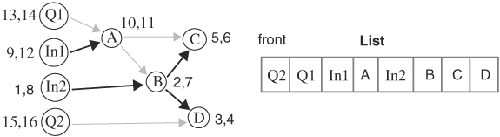
We need to understand why the algorithm guarantees that a gate be placed after all its fanin gates. When a gate’s fanin is reached, either the gate has been visited or not. If the gate has already been visited, the gate must have been already inserted in List. Because insertion to List is always in the front of List, the fanin will be inserted before the gate when the fanin is inserted. If the gate has not yet been visited, the gate will be finished visiting first before the fanin can be inserted into List. This is because all fanouts of the fanin must return from VISIT, as indicated in the for_each loop of the VISIT part of the algorithm. Hence, the fanin is again before the gate in List. This argument applies to any fanin. Therefore, the order in List guarantees that a gate be after all its fanins.
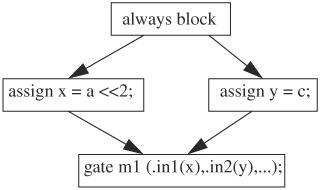
So far, we have discussed levelization in the context of a gate model. The algorithm applies to RTL models as well. First, the RTL model must be leveled by constructing a graph representing the model. The key in constructing such a graph lies in identifying the fanins and fanouts of the RTL constructs. The RTL constructs include gates, blocking and nonblocking assignments, system and user tasks, and monitors. The order produced by the topological sort only mandates that fanins be evaluated before the gate itself. The stratified event queue in the IEEE 1364 standard further imposes an ordering constraint on RTL constructs, such as nonblocking assignments, system and user tasks, and monitors. Let us call this group of constructs end-time group. This constraint requires that the end-time group of constructs be evaluated last and, within the group, nonblocking assignments are executed first, followed by system and user tasks, and finally monitors. Therefore, gates, continuous assigns, and blocking statements are scheduled according to the order in which the gates are leveled. After they have been evaluated, the end-time group is evaluated. User/system tasks with outputs that are used by other parts of the circuit before the end of the cycle must be executed at the time they are called, instead of moved to the end of the cycle.
As a side product, topological sort detects loops. (More precisely, DFS detects loops.) In the case of circuit simulation, a combinational loop exists if the topological sort detects a loop in the circuit graph with FFs and latches removed. Before discussing loop detection, let us first define some terms. Vertex A is called a descendant of vertex B if A can be reached, following directed edges, from B in a DFS tree. Vertex B is called an ancestor of A. A back edge is an edge that goes from a descendant to an ancestor. A loop exists if and only if there is a back edge.

Although applying a topological sort to a circuit with combinational loops will produce a list of ordered nodes, the order can no longer guarantee that all fanins of any gate be placed before the gate itself. This is because any two gates in a loop have each other as a transitive fanin. So no matter how they position in the list, one gate will be evaluated before the other, which, as a transitive fanin, must have been evaluated first. An impossible situation results. Therefore, cycle-based simulators cannot simulate correctly circuits with combinational loops. (By grouping loops into strongly connected components (SCCs), a circuit with combinational loops can be transformed into one without loops and hence can be addressed by a cycle-based simulator if the SCCs are simulated separately. A later section on levelized compiled simulators discusses this in more detail.)
So far we have assumed that the entire circuit has only one clock and that all logic between FFs and latches is evaluated once every cycle. When a circuit has multiple clocks, not all logic has to be evaluated at every clock transition—only the part that is triggered by the clock transition. That is, we have to determine the part of the circuit that requires evaluation at each clock’s transition. This task is called clock domain analysis, and the set of components that are evaluated at a clock’s transition is the domain of the clock.
To find a clock’s domain, we first identify all FFs and latches triggered by it. For these FFs and latches to store the correct values at the triggering transition of the clock, all logic converging at their inputs must be evaluated just before the clock transition. A clock triggering transition is the one that locks a value into an FF or a latch (for example, a rising transition for a positive-trigger FF and a falling transition for a high-sensitive latch). Therefore, a clock can potentially have two clock domains, one for a rising transition and another for a falling transition. We see later that these two domains are not necessarily identical. To find the logic cone for a given FF or latch, we back trace from its input until we arrive at either a primary input, an FF, or an opaque latch. The reason why we stop at an opaque latch but not a transparent latch is that only an opaque latch’s output value is a steady-state value of the latch. If back tracing eventually stops, which is guaranteed if no combinational or latch loops were encountered, then all the logic traversed forms a clock domain. This procedure is then applied to both transitions of every clock. After all the clock domains are determined, they are leveled and evaluated at their associated clock transitions. The following summarizes this domain partitioning algorithm:
After all clock domains have been identified and leveled, evaluation of the clock domains is triggered by clock transitions. When a clock transition occurs, its corresponding clock domain is executed according to its levelized order. When it finishes, it returns and waits on the next clock transition or a user interrupt. Before calculating clock transitions, the clock logic or clock tree that supplies the clock waveforms has to be identified first. A clock tree is the part of the circuit that is bounded by clock pins and primary inputs, and is usually made up of only simple combinational gates. A sample clock tree is shown in Figure 3.14.
The functional procedures discussed earlier are executed in the following sequence. After the input circuit is parsed and elaborated, its clock tree is traced out and the clock waveforms are computed. Then, for each clock transition polarity (falling and rising), its domain is carved out and levelized. At the various stages, optimization may be applied to increase code performance. An example is to prune logic that is not driving any output, and to collapse buffers. At this point, the result is ready for code generation.
Code generation produces code that executes to simulate the circuit with cycle-to-cycle accuracy. As mentioned earlier in the chapter, there are four types of generated code: interpreted, high level, native, and emulator. Here we look at code generation by creating high-level code. Generated code performs all the operations of a simulator and thus has all the components described in Figure 3.4, such as clock waveforms, circuit connectivity, component functionality, storage space for circuit node values, a time advancement mechanism, and a facility to read and write node values.
For the user interface, embedded in generated code are communication channels to simulation control, through which the user can specify the length of the circuit simulation, pause the simulation when a condition is met, and inspect node values. The communication channels can be memory locations of variables that simulation control can deposit values (for example, number of cycles to simulate), or wait statements where the simulation waits on commands from the user.
Furthermore, system/user tasks can be implemented as either part of the compiled code or as a dynamically loadable library. With the former, the generated code contains the object code of the tasks. A call to a task is a jump to the task’s entry point. With the latter, the generated code simply has in the place of a system/user task, a call to simulation control with the name of the task. The simulation control, when called, dynamically loads the code segment of the task from the library and executes the task. In this implementation, system/user tasks are compiled independently of the circuit. Figure 3.15 shows the flow of generated cycle-based code.

To start the simulation, the user invokes the simulation control to load the generated code, specifies a number of conditions and parameters (for example, the number of cycles to simulate, or a break point condition such as stop if Node1.value == 1’b1, and starts the execution. The generated code runs until one of the specified conditions or parameters fires, or the end of the simulation is reached. During the simulation, communication between the simulation job and the simulation control may take place—for instance, displaying error messages from the simulation to the console or handling system/user task calls using a dynamically loaded library. When the simulation is paused, the user may inquire about node values, may step cycle by cycle, or may save the simulation state to be restored in a later session.
So far, we have discussed two simulators at the extremes: event-driven and cycle-based simulators. The former is versatile but slow; the latter is fast but restrictive. It is possible to construct a simulator tailored for specific requirements that lays in the middle of the simulator spectrum. Simulator characteristics (such as event driven, levelized, compiled, interpreted, and centralized or distributed event schedule) are independent of each other and hence can be chosen individually to concoct a hybrid simulator. A simulator can be designed to be levelized, event driven in nature, but with some components compiled, and can have a centralized event scheduler. On the other hand, a simulator can be constructed so that each of its clock domains is levelized and it runs like a cycle-based simulator, but the interaction among the domains is event driven. In the following sections we will look at several typical hybrid simulator designs.
With this combination, components of the circuit are compiled code. However, triggering the evaluation of a component and thus execution of its compiled code is dictated by the events among the components. The granularity of components in this case is not necessarily a single gate or RTL construct. It can be a group of gates or RTL constructs. The finer the granularity of the component, the closer the simulator is to being a true event-driven simulator.
Levelization is not a technique used solely for cycle-based simulation. It can also be applied to event-driven simulation. In the previous discussion of event-driven simulation, we assumed an arbitrary order of execution of events occurring at the same time, except for nonblocking assignments and monitors, which are executed at the end of the current simulation time, as specified in the IEEE Verilog standard. Now we will see how event prioritization can improve event-driven simulator performance.
Consider simulating the zero-delay circuit and input events in Figure 3.16. If we follow the usual event-driven scheduling algorithm, the event evaluation order would be e1, e2, e3, and e4, followed by the output events on gates A, B, D, and C. The widths of the pulses are exaggerated to illustrate the number of evaluations induced by them. They are zero in actual simulation. A gate is evaluated once for every input event; therefore, there is a total of nine evaluations. Because all glitches have zero widths, oftentimes the user is only interested in the steady-state values. Therefore, only steady-state values are of concern, and levelization can prune away transient evaluations. For example, gate D can compute its steady-state output by delaying its evaluation until gate B is done evaluating. In general, a gate should be evaluated only after all its input gates have finished, which is exactly what a levelized order guarantees. If a leveled order is imposed on event scheduling, gate A is evaluated first, followed by B, then D, and finally C, giving a total of only four evaluations.
To incorporate levelization into event scheduling in a zero-delay simulation, the circuit is first leveled and then the event queues are sorted by level. At simulation time T, events from the level 1 queue are evaluated first. If events are generated at a component’s output, the events are inserted in the queues corresponding to the level of the fanout gates. Events are evaluated one level at a time. When queues at all levels are finished, time advances. In a timing wheel, each time slot is modified to hold queues, one for each level. A levelized event driven for a zero-delay simulating scheduling algorithm is as follows:
This levelized event-scheduling technique resembles cycle-based simulation, but the main difference is that cycle-based simulation evaluates all circuit components whereas this levelized event-driven algorithm evaluates only the ones with input events. For instance, if events e1 and e3 in the previous example are absent, a levelized event-driven simulator will only evaluate gate D, whereas a cycle-based simulator will evaluate all four gates. The similarity between these two types of simulator is that, if a gate is evaluated, it is evaluated just once in both types of simulators.
In a previous discussion, we noted that a cycle-based simulator cannot accept a circuit with combinational loops. This restriction can be relaxed if a hybrid method is used. If we think a little deeper about cycle-based simulation, we would notice that FFs and latches are essentially combinational loops, but they are simulated in cycle-based simulators. Thus, we can conclude that combinational loops can be simulated by a cycle-based simulator if they can be encapsulated into macro models. To extend the scope of cycle-based simulation, all combinational loops should be encapsulated in macro models, and the macro models should be simulated using an event-driven simulator, so that the circuit with the macro models can be simulated with a cycle-based simulator. The next question is how to find and isolate all combinational loops. The following algorithm isolates all loops and guarantees that the resulting circuit with the loops encapsulated is loop free.
An SCC of a directed graph is a maximal subgraph such that every node can be reached from any other node. The SCC is an expanded notion of a loop. A directed acyclic graph (DAC) is a tree or forest, and hence is free of SCCs. It is known that any directed graph can be decomposed into a DAC and SCCs. In other words, this decomposition breaks any directed graph into looping components and straight components. Once a graph is decomposed in such a way and the SCCs are encapsulated, the resulting graph is a DAC, and is loop free. SCCs can be determined by applying DFS, as follows:
In step 2, “reversing an edge” means making the head of the edge the tail, and vice versa. When applying DFS to this graph, in the while loop of the DFS algorithm (see page 91), select unvisited nodes in the order of decreasing exit numbers, which were derived in step 1.

Figure 3.17. Finding SCCs. (A) Result of a DFS. The underlined numbers are exit times. (B) DFS on the graph derived by reversing the edges. (C) Resulting DAC by treating SCCs as composite nodes.
When the SCCs are found, they are compiled individually and are treated as macro models. The resulting circuit is free of combinational loops and can be simulated with a cycle-based simulator. During simulation, if an SCC macro model is encountered, its compiled code is called to perform its own evaluation, very much like FFs and latches are simulated.

A major cause of slow simulation performance in event-driven simulators is the centralized event manager: the timing wheel and its maintenance. To mitigate this problem, the centralized event manager is replaced by multiple distributed local event managers embedded in partitioned domains, each of which is in charge of its own domain. Cross-domain events are handled by a global event manager. An event domain can be a clock domain in circuits with multiple clocks, or an instance at the unit granularity level. A key indicator for an effective event domain partition is minimal cross-domain events. Such a simulator gains performance when run on a multiple-processor machine.
Hardware simulators and emulators are computers that are specially designed for running simulations. An emulator is just a simulator with an interface connected to a hardware system as a substitute for the circuit being simulated. When the system operates in real time, the emulator takes in input signals, computes the outputs, and responds with the results, all in real time. Hence, emulators have more stringent response time requirements than simulators. Besides, there are no major differences between the two. For this reason, we only discuss hardware simulators in this section.
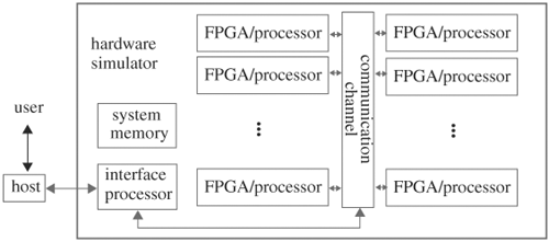
There are two types of hardware simulators, classified by their underlying hardware computing components: one is FPGA based and the other is processor array based. The FPGAs or processors can be connected in any network configuration, but the common ones are two- or three-dimensional mesh or torus, where processors are placed on grids and connected along the grid lines. A torus is a mesh with the ends wrapped around (see Figure 3.19). Another common configuration is through a central switch, such as a crossbar or butterfly switch, or a simple bus. The user interface is often through a host machine that in turn is connected to the simulator. A block diagram of a generic hardware simulator using a central switch is shown in Figure 3.20.

In an FPGA-based architecture, each FPGA chip has a network of prewired blocks of look-up tables and a bank of FFs. A look-up table can be programmed to be a Boolean function, and the look-up tables can be programmed to connect or bypass the FFs. If connected, the FPGA chip operates as a finite-state machine. If bypassed, the FPGA chip operates as a combinational circuit. The look-up tables can be programmed to mimic any combinational logic of a predetermined number of inputs and outputs. To run a circuit on an FPGA-based simulator, the circuit must first be compiled. A compiler partitions the circuit into pieces, each fitting into an FPGA chip. The partitioned subcircuits are then synthesized into the look-up tables (that is, generating the contents in the look-up tables such that the look-up tables together produce the function of the partitioned subcircuits). Then the partitioned netlist is placed and routed on the FPGA chips. In other words, we assign the subcircuits to the chips and connect the chips in a way that preserves the connectivity in the original circuit.
Similarly for a processor array-based architecture, the input circuit is partitioned into subcircuits so that each piece fits the instruction memory of a processor. Besides instruction memory, each processor also has data memory. The code running on a processor can be either event-driven or cycle-based code. After the code is loaded into the processors, the processors simulate their respective portions of the circuit. At predefined times, the processors propagate and synchronize their results, in effect simulating the input and output flow of signals among the partitioned subcircuits. In cycle-based simulation, synchronization occurs at the end of the cycle, whereas in event-driven simulation, it occurs when cross-domain events happen.
In summary, a hardware simulator compiler follows very much the same flow as a software simulator compiler. The major difference is that it has a partitioner to break down a large circuit and a scheduler to set up communication among the computing resources. Hardware compilation can generate event-driven code or compiled code. In the event-driven case, event management can be centralized to a processor or it can be distributed among processors. Furthermore, hardware simulators can only verify logical functionality but not timing properties, because delays from a network of FPGAs or processors do not correlate with those in the design.
After compilation is done, the compiled image is downloaded via the interface processor to the hardware. Besides downloading compiled images, the interface processor also uploads simulation results, controls the simulator in interactive mode, calls the host to execute system functions or tasks, and passes the results back to the simulator. Each processor has its own instruction and data memory. In addition, there may be system memory that can be used to model the memory arrays in the circuit.
Although a new type of simulator results with each combination of the simulator architectural features, there are only a few in use. Let’s study their relative strengths and limitations, and survey their application arenas.
In a two-state simulator, a node can have the value 0 or 1, whereas in a four-state simulator it can have 0, 1, x, and z, where x denotes an unknown value and z denotes high impedance. An x value results when a node is uninitialized or two sources are driving the node to opposite values at the same time. A z value results when all drivers on a bus are brought to high inpedance. If an x or z value is encountered in a two-state simulation, it is mapped to either 1 or 0. For the following discussion, let’s assume that the x and z values are mapped to 0.
The algebra of x and z can be summarized as follows: If an input is either x or z and other inputs do not have a controlling value, the output is x. If an input has a controlling value, the output is then determined by the controlling value. A controlling input value determines the output of the gate independent of other input values. For example, 1 is the controlling value of the OR gate, and 0 is that of the AND gate. The complement of x is x. The complement of z is x.
The algebra of x and z can produce pessimism in simulation results. A well-known example is that of a multiplexor. The following RTL code is a multiplexor. When s = 0, output y = j. When s = 1, y = i.
assign n = i & s;
assign m = j & (~s);
assign y = n | m;
If s takes on an unknown value x, and inputs i and j are both 1, then one might reason that, because output y is either i or j, and i = j = 1, y should be 1 regardless of the value of s. However, if output y is computed according to the algebra of x and z, a different value results. Because both s and ~s are of value x—the complement of x is x—and both i and j are 1,n and m have x value, giving an x value to y. The cause of this pessimistic result is the result of the rule that the complement of x is x. Making the complement of x to be ![]() only complicates matters.
only complicates matters.
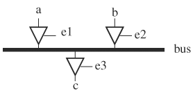
In two-state simulation, high impedance, bus contention, and a zero value on a bus are all mapped to 0. Sometimes, the simulator needs to distinguish these situations, such as when detecting errors on a bus and determining whether a true zero or high impedance is read from a bus. Knowing the value of all bus drivers’ enable pin and the input values distinguishes these situations. Bus contention occurs if more than one driver is enabled, and inputs to the drivers are opposite. The bus is in high impedance if no bus driver is being enabled and there is neither a pull-up nor a pull-down. The bus has a true zero value if only one driver is enabled.
A two-state simulator is faster, because evaluations are shorter and storage is smaller with two values. A four-state simulator is normally used to simulate the power-up period, when many states are uninitialized. After a while, a well-designed system will be free of unknown states. Then, a two-state simulator can switch to replace the four-state simulator and can continue the simulation at a faster speed.
A zero-delay simulator ignores all delays in the circuit and is used mainly for functional verification. A unit-delay simulator assumes that all gates have a delay of one. Unit-delay simulation generates orders of magnitude more events than zero-delay simulation, because all glitches that are collapsed into a single transition in a zero-delay model may now occur at different times (see “Leveled event processing for zero-delay simulation” on page 101). Therefore, zero-delay simulators run much faster. Unit-delay simulation aims at hazard and race detection. The unit delay is introduced to “spread” out transitions so that glitches and race problems are revealed. A design with realistic delays, back annotated from layout information, provides more accurate timing information but runs even slower because more events may surface as the delays spread out the glitches further. Note the separations between transitions arising from three delay models—zero, unit, and real delay—as shown in Figure 3.21. Unit-delay simulation is very useful for detecting reset problems and logic where the RTL and gates do not match, because it is much faster to simulate than a full-delay model.
The main cause of slow performance in event-driven simulators is centralized event management, whereas the potential performance drawback in cycle-based simulators is the indiscriminate simulation of all components, regardless of input excitation. Empirical data have shown that unless switching activity inside a circuit is less than 1% (the percentage of nodes switching), cycle-based simulators are faster. In practice, the average switching activity is around 10 to 20%, which translates to 5 to 20 times acceleration. However, cycle-based simulators have a more stringent coding style. They cannot simulate asynchronous circuits, timing behavior of circuits with delays, and some test bench constructs, just to name a few. Moreover, it takes longer to compile a circuit for cycle-based simulation. Therefore, cycle-based simulators are ideal for functional verification, whereas event-driven simulators are more suitable for timing verification and prototyping.
Compiled simulators have better simulation performance but take longer to compile, are less interactive, and are less portable. Interpreted simulators find usage in prototyping, where speedy compilation and accessibility to internal nodes are a premium. Compiled simulation optimizes much for performance and destroys more user-entered structure. Interpreted simulation also finds its strength in intellectual property (IP) procurement. An IP design can have various levels of implementation—from an RTL netlist to a simulatable binary model to a layout of the design. If an IP only offers simulation functionality but not its implementation details (for example, a functional model of a hardware core), the seller can ship the IP in a precompiled format compatible with a standard interface (such as SWIFT), so that the content is protected yet the user can execute the precompiled code using any interpreted simulator accepting the standard interface.
Hardware simulators are often a few hundred to a few thousand times faster than software simulators. However, improper design of a test bench (for example, extensive interaction between the host and the simulator) or improper use (for example, heavy dumping of signals) can drastically decrease the performance to that of software simulation. Therefore, a major bottleneck for which to watch when using a hardware simulator is the interaction between the hardware simulator and the host. To minimize interaction, data exchange is often cached and flushed all at once, when it is full. Aside from performance, hardware simulators fall short of their software counterparts in the scope of design constructs that can be simulated, inability to verify timing properties, and ease of debugging.
The critical characteristics of a hardware simulator are capacity, speed, compilation time, and debugability. With today’s technology, processor-based simulators have a higher capacity than FPGA-based simulators, but they are more complex to design. Performance-wise, they are comparable. For hardware simulators, compilation time is a major factor for application consideration, because it can be 5 to 50 times longer than software compilation. The bottleneck comes from partitioning the design, placing components, and routing signals among the components. Oftentimes, large designs require intervention from the user to complete compilation. Consequently, hardware compilers should be able to compile incrementally. Between FPGA and processor array accelerators, FPGA accelerators have much slower compile time, and processor array accelerators have compile times approaching to those of software simulators. Designs run on a hardware simulator should be optimized to have a minimum amount of output data. Finally, because hardware simulators are a rare resource shared by many, in addition to their limited circuit node visibility, debugging directly on a hardware simulator is counterproductive. A solution to this is to save the state of the simulation, when errors are detected, and load the saved image to a software simulator, where debugging can conveniently proceed.
Table 3.1 summarizes the relative effects of several simulator architectures on performance, capacity, compile time, debugability, and portability. If a feature has no directly significant impact, it is labeled as NDI. Four grades are used: best, better, NDI, and worse.
Table 3.1. Relative Effects of Simulator Architectural Features on Five Qualities of Simulator
Feature | Event driven | Interpreted | High level | Native | Levelized | Hardware |
|---|---|---|---|---|---|---|
Performance | Worse | Worse | Better | Better | Better | Best |
Capacity | Better | Better | Best | Better | NDI | Worse |
Compile time | Best | Best | Better | Better | Better | Worse |
Debugability | Best | Best | Worse | Better | NDI | Worse |
Portability | Better | Best | Better | Worse | NDI | Worse |
This section studies typical features in a simulator and where these features are applicable. This section is not meant to be a substitute for simulator manuals, but rather it serves to introduce the concepts and commands that are available in a simulator. It is not feasible to cover all simulator commands, because of their enormous number and variation over simulators and time. However, simulator commands are just an embodiment of more fundamental concepts. It is these concepts that are precisely the focus of our study in this section. Therefore, the commands in this section are pseudocommands. Besides explaining functions in command categories, we will also discuss how commands are applied.
Every simulator has a directory structure for input, output, and command files. The input directory, which usually has subdirectories, holds HDL design files, include files, library files, Makefiles, compiled images, and sometimes C/C++ files for PLIs. The HDL design directory often has subdirectories corresponding to the functional units of the design. Within a functional unit subdirectory are design files that contain RTL code, along with macros, parameters, and constant definitions, which reside in include files. The library file contains cell definitions, such as FFs and encoders. A cell is defined to be the module lowest in the design hierarchy and there is no module instantiation inside it. Makefiles perform various tasks such as compiling C/C++ code and linking object code to produce executables, expanding macros to generate HDL files, and compiling the design for simulation. Compiled images are files produced by the simulator’s compiler and are input to the simulator. The output directory, possibly having a couple layers of subdirectories, contains log files generated from simulation runs, signal tracing files, error logs, and others. The command directory has script files for simulation compilation, simulation run, debugging options, and others. An example simulation directory organization is shown in Figure 3.22.

To guide a simulator or compiler to search for a file or a directory, the information is passed through runtime options. For example, to specify an input file or to designate an output file, a full path to the file is specified on the command line, or the directory holding the files is passed as option arguments and the simulator or compiler searches the files. If directories are passed, the compiler searches files in the current working directory and then the specified directories. A typical command line for compilation may look like
compile −f filelist −y srcDirectory +option1 +define+MyVar=1
−output=logFile −o sim
where filelist contains paths to the HDL design files and include directories. The following is an example:
+incdir+/home/design/include/
+incdir+/home/design/macro/
/home/design/adder.v
/home/design/multiplier.v
...
The first two lines specify the include directories to be /home/design/include and /home/design/macro/ so that when an include file is encountered during compilation, these two directories will be searched. The remaining files are HDL design files. The argument after −y is the directory for library cells. The next item, +option1, can be any option known to the compiler. The next item, +define+MyVar=1, sets the value of the compile time variable MyVar to 1, so that whenever MyVar is encountered in the source files during compilation, it is replaced by 1. The next item designates logFile to be the output file. Finally, the last item specifies the name of the compiled image to be sim. After compilation, the simulator can be invoked using a command such as
simulate −image sim +option2
where the simulator loads the compiled image file sim and takes in runtime option option2.
In this section we discuss simulator options for enhancing performance and debugability of the circuit. Options for performance and for debugability have opposite effects on simulation: High performance means less debugability and vice versa. This is because to increase simulation speed, the circuit representation often needs to be restructured. For instance, buffers and inverters are combined with other gates and are eliminated, bus bits are aggregated, redundant logic is pruned, and blocks with the same sensitivity are merged. Consequently, the eliminated nodes are not observable, and the resulting structure is not easily recognizable to the user, making the circuit more difficult to debug.
Most simulators have several levels of performance optimization. We assume the highest level means the highest performance and hence the lowest degree of debugability. Debugability usually refers to how the user may inquire or manipulate circuit nodes or variables during simulation runtime or through user PLI tasks. Different modules in a design can be tailored to have different levels of optimization so that the well-tested modules can be optimized to the greatest extent. At different levels of optimization, the corresponding debugging restrictions imposed at each level vary. An example guideline follows. At the highest level, nodes or variables can only be read. At the next level, values of nodes and variables can be modified, and delays of gates can be altered. Changing a node value can be done, for example, by using Verilog’s force construct, or PLI’s tf_put, or by assigning to a new value during an interactive simulation session. At the lowest level, all performance optimizations are disabled, and everything is readable, writable, and traceable. Traceable means that the circuit structure can be traversed through PLI routines (for example, inquiring about fanouts or fanins of a node through PLI’s acc_next_driver or VPI’s vpi_iterate). Obviously, to enable traceability, the simulator must maintain a mechanism to support the PLI or the VPI routines, which slows down performance. If a node or a variable is accessed at a level not permissible by the optimization option (for example, if it is assigned a new value while the highest performance option is specified), an error will result. An example compile command with tailored optimization options is as follows:
compile −f filelist +optimize+level2+file=ALU.v +optimize+level1
where the first optimization option specifies that file ALU.v be optimized at level 2 and the rest optimized at level 1.
To debug a circuit, viewing signal waveforms is a necessity. A common practice is to dump out signal traces during a simulation run and view them later with a waveform viewer. Using this method, the user can debug off-line and free up the simulator for others. Unless all resources have been exhausted, it is inefficient to dump out all signal traces in the design, especially when the design is large. Instead, only a portion of the design is selected for dumping, and this selection can be made by the user during compilation or simulation. To implement selective dumping at compilation, Verilog’s ifdef guards a dumping code segment that can be activated to dump signals in a functional unit. When the variable of ifdef is defined, the dumping code is activated. If the code is not activated, signals from the unit are not dumped. For example, to create selective dumping for functional unit ALU, the following code is used:
'ifdef DEBUG_ALU
   $dumpvar(0, alu);
'endif
System task $dumpvar dumps out all node values inside module alu in value change dump (VCD) format. The first argument, 0, means that all levels of hierarchy inside alu are dumped. To activate this task at compile time, the following command is used, which defines variable DEBUG_ALU:
compile −f filelist +define+DEBUG_ALU ...
Because variable DEBUG_ALU is defined, the code $dumpvar(alu) is compiled with the rest of the circuit, and dumping is activated. Dumping can also be activated during simulation runtime and it is done via plusarg (short for +argument). Change the previous ifdef to the following if statement:
if($test$plusargs(debug_alu == 1))
   $dumpvar(0, alu);
where task $test$plusargs checks the value of argument debug_alu. If it is equal to 1, the following line will be executed. To invoke this dumping at runtime, the simulator is invoked with the plus argument +debug_alu+1:
simulate −image sim +debug_alu+1
plusarg +debug_alu+1 defines the value of the argument to be 1, and hence turns on dumping of alu.
The differences between compilation time and simulation time selection are the size of the compiled image and the ability to select dumping based on actual simulation results. If a dumping code is implemented as a compilation time option, the decision to dump (or not) must be made at compilation time. Once compiled, it cannot be changed without recompilation. The advantage is that, if selected not to dump, the resulting compiled image is smaller. On the hand, if it is implemented as a simulation time option, what to dump can be decided when a bug shows up, without recompiling. The disadvantage is that the code has already been compiled, even though it is selected not to dump.
Table 3.2 summarizes the effects of simulator options on compilation and simulation speed, as well as debugging capability.
Table 3.2. Effects of Simulator Options on Compilation and Simulation Speed and Debugability
Option Type | Effects |
|---|---|
Enable read, write, and connectivity trace | Slow down compilation and simulation but increase debugging capability |
Enable two-state simulation | Speed up both compilation and simulation but decrease debugability |
Disable timing checks | Speed up simulation but decrease debugability |
Use a zero-delay or a unit-delay model | Speed up both compilation and simulation but decrease debugability |
Perform structural optimization (combine bits, eliminate buffers) | Slow down compilation, speed up simulation, and decrease debugability |
Enable interactive simulation | Slow down compilation and simulation but increase debugability |
To verify timing properties, a delay model for the circuit must first be chosen. One delay model is a zero-delay model, in which all gates and blocks, specified explicitly or not, are assumed to have zero delays. This delay model does not reveal much timing property about the circuit and thus is used mainly for functional verification. A zero-delay model produces the fastest simulation speed compared with other delay models. Another model is a unit-delay model for which all gates and blocks have a delay of one, and all specified delays are converted to unit delays. This delay model is not realistic, but it is a reasonable compromise between a realistic but slow delay model and the zero-delay model. Its main application is in detecting hazards. Finally, a full-delay model allows each gate, block, and interconnect to have its own delay. The delay values are usually extracted from the layout of the design and are back annotated to the design for timing simulation. This full model has the most accurate timing information, but it runs the slowest. It is used for timing closure verification after functional verification is completed.
To build a full-delay model, delay information on gates and interconnects is computed based on the cell library and RC extractions from the design’s layout. The delay numbers used in timing simulation are interconnect delays and gate propagation delays.
Interconnect delays are calculated from the interconnect’s physical dimension and the resistive and capacitive parameters of the IC fabrication process. Gate delay is determined by three variables: input transition speed, delay equation of the gate, and output capacitive load. A steeper input transition produces a smaller gate delay. A larger capacitive load causes a larger gate delay. A delay equation of a gate takes in an input transition speed and an output load, and produces the gate’s delay and the output transition speed. A gate’s delay equation is obtained by characterizing the gate using a transistor-level simulator, such as SPICE. The characterization process simulates and measures the gate’s propagation delays and output transition speeds for a range of input transition speeds and output capacitive loads. The measures are then fit into a set of equations.
To calculate a gate’s delay in a layout, the gate’s input and output capacitance are first extracted from the layout. Next, the input transition speed is calculated by computing the output transition speed of the driver on the gate’s input capacitance using the driver’s delay equation. With this input speed and the gate’s output capacitance, the gate’s propagation delay is calculated using the gate’s delay equation. This iterative process is captured in Figure 3.23.

The calculated delays numbers, gate and interconnect, are then stored in standard delay file (SDF) format. The exact format can be found in the OVL Standard Delay File (SDF) Format Manual. These delays are then written and annotated to the gate or block models using Verilog’s #delay construct or specify/endspecify construct.
A delay model can be selected as an option in the command line or as a compiler directive. When both are present, the former takes precedence over the latter. The exact syntax for delay model selection is not an IEEE standard, and thus is simulator specific. An example of delay model selection is as follows:
compile -f filelist -unit_delay_model // command-line option
selecting unit delay model
or as compiler directive ’use_unit_delay_model inside the HLD code. Both keywords unit_delay_model and use_unit_delay_model are understood by the compiler to choose the unit-delay model.
So far, we have assumed a single number of gate delays. As a part of the IEEE standard, a delay can have three possible values: minimum, typical, and maximum. A gate with a delay triplet is declared as follows, in which its minimum is 1; typical, 1.2; and maximum, 1.5:
buffer #(1:1.2:1.5) gate1(...);
Which delay value is to be used in simulation can be selected by passing a simulator-specific option to the compiler, such as
compile -f filelist -typical_delay
// command option selecting typical delay among maximum,
typical, and minimum delays
Once a delay model is selected, a simulator can be configured to verify various timing properties. Some common properties are timing checks, race check, and narrow pulse check. There are eight IEEE standard built-in timing checks in Verilog: $setup, $hold, $setuphold, $width, $period, $skew, $nochange, and $recovery (based on IEEE 1364–1995). These timing checks perform three tasks: (1) determine the elapsed time between two events, (2) compare the elapsed time with a specified limit, and (3) report a timing error if the limit is violated. For example, $setup(data_in, psedge clock, 1) compares the time elapsed between a transition of signal data_in and a rising edge of clock. If the elapsed time is less than one unit of time, a violation will be reported. The same applies to $hold and $setuphold.$width checks for pulses with a width narrower than a specified limit—glitch detection. $period flags an error if the period of the signal is smaller than a specified limit. $skew issues an error if the time interval between two transitions (the skew) is greater than a specified limit. Finally, $recover checks for the recovery time of a changed signal, whereas $nochange checks for a steady-state value of a signal within a time interval. For instance, $nochange (posedge clock, data, 0, 0) issues an error if data changes while clock is rising. For a more detailed description of these checks, please refer to IEEE 1364-1995 or later version. A simulator can be configured to perform timing checks on selected modules. For example, the following command passes in a file, timing_file, that specifies which modules should be skipped for timing checks or which block delays should be replaced with zero delays:
compile -f filelist -timing timing_file
A typical format for timing_file is
<module path> <timing specification>
an example of which is
top_module.* no_timing_checks,
meaning all submodules under top_module should be skipped for timing checks.
In a real circuit, every transition has either a nonzero rise time or a nonzero fall time, and consequently it is possible that the finite rise and fall times shape a narrow pulse so that it does not have enough energy to propagate through a gate, as seen in Figure 3.24. This phenomenon is called narrow pulse filtering.

Figure 3.24. Effect of nonzero rise and fall times on narrow pulses. (A) A narrow pulse is filtered out. (B) Two closely spaced transitions fail to propagate the glitch.
RTL simulators combine rise and fall times with gate propagation delay, and use the combined delay as the overall gate delay. Effectively, all transitions have zero rise and fall times. Most simulators have a mechanism to detect narrow pulses. First, let us define some terms. The gate delay measured from an input transition to an output transition is called the transport delay. The minimum width a pulse must have to propagate to an output is called the inertial delay. The narrow pulse filtering effect is modeled by inertial delay. A common practice is to filter out automatically pulses of a width less than or equal to the delay of the gate (transport delay = inertial delay). To override this, the user can pass, in compile time, options specifying a limit on the minimum pulse width, in terms of a percentage of gate delay. Furthermore, this option can be applied to selected modules or paths. An example command follows:
compile -f filelist -pulse_width_limit=50 -pathpulse ...
where -pulse_width_limit=50 sets the minimum pulse width to be 50% of the gate delay, and -pathpulse enables module path-specific pulse control rules. Module path-specific pulse control rules specify pulse widths for paths inside a module. The rules are embedded in RTL code within specparam with a keyword such as PATHPULSE$ = 5, meaning the minimum pulse width for the module is five units of time.
When a pulse violates a pulse control restriction (for example, a pulse width is narrower than the inertial delay) the output of the gate becomes unknown. When this situation occurs, the time that the output becomes unknown can be determined using two methods. The first method, called alert on output transition, sets the time of unknown output to be the time when the first edge of the input pulse appears at the output. The rationale is that this is the time the output recognizes the input pulse. The second method, called alert on detection, sets the time of unknown output to be at the moment the input pulse is determined to be in violation. The rationale here is that this is the time the violation occurs. Most simulators allow the user to choose either method of reporting. Figure 3.25 illustrates the two reporting methods. The pulse at input in of the invertor has a width of 2, whereas the gate has an inertial delay of 3. Therefore, this pulse will flag an error. The transport delay of the gate is 3. View A in Figure 3.25 illustrates the rule of method 1. It produces an unknown output (shaded region) when the first transition of the input pulse has propagated to the output, which happens at time 5. The unknown value lasts until the second transition gets to the output, which occurs at time 7. View B illustrates the rule of method 2. It sends the output to unknown once the pulse is detected to be narrow. The detection time is when the second edge of the pulse arrives at the input, which is at time 3. This unknown value persists until the second edge of the pulse has reached the output at time 7.

Design profiling gathers information on how simulation time is distributed throughout the design and underlying supporting operating system (OS). The main purpose of using design profiling is to find simulation bottlenecks and optimize them for performance improvement. Activating profiling slows down simulation speed.
Profiling results can be collected at various levels of the design hierarchy. A profiling result in a design scope is sometimes called a view. One view is the overall summary of computing times spent on the design, the OS kernel, PLI calls, and signal dumping. An example of an overall view is shown in Table 3.3, where the design took 313.2 seconds, about 36% of the total simulation time. OS kernel time is the time spent on calling OS system tasks such as those for file I/O. PLI task time is that used by PLI tasks. Signal trace dumping is a major consumption of simulation time (for example, dumping VCD files).
Table 3.3. Example Simulation Profiling Summary
Scope | Total Time, sec | Time, % |
|---|---|---|
Design | 313.2 | 36 |
OS kernel | 72.4 | 8 |
PLI tasks | 155.7 | 17 |
Signal trace dumping | 322.9 | 39 |
Inside a design view, there can be more scope. Examples include the module view, where runtime distribution statistics on modules are collected, and the construct view, where statistics on always blocks, continuous assignments, functions/tasks, timing checks, UDPs, and other constructs are gathered. In the construct view, each construct is identified by filename and line number. An example of a construct view is shown in Table 3.4. For example, 2.9% of time is spent on an always block in file chip.v on lines 122 to 244.
Table 3.4. Profiling Statistics of Constructs of a Design
Construct | Instance | Time, % |
|---|---|---|
| chip.v: 122-244 chip.v: 332-456 | 2.9 3.3 |
| reset.v: 100-144 | 2.5 |
Function | ecc.v 320-544 m ask.v: 124-235 | 2.0 1.3 |
Task | cache.v: 212-326 | 1.9 |
Timing check | pipeline.v: 32 | 0.4 |
To activate design profiling, an argument is passed to the compiler so that the mechanism to collect the statistics can be constructed and compiled during compilation, such as
compile -f filelist +profiling ...
Two-state simulation is faster but four-state simulation detects unknown and high-impedance states better. Some simulators allow users to specify at compilation time with an option such as +two_state whether two-state or four-state simulation is to be executed. When simulating in two state, some simulators convert the entire design to a two-state version by replacing x and z with 0, and ignoring the unconvertible constructs. Therefore, for these simulators, the result from the unconvertible constructs may be wrong. Some simulators, on the other hand, preserve certain constructs that are inherently four state. For these simulators, the acceleration is less. Therefore, when coding for simulation performance, it is important to know what constructs are inherently four state. The following is a list of four-state constructs.
Strength data types. Verilog data types
tri1andtri0model nets with implicit resistive pull-up and pull-down. If no driver is drivingtri1, the value oftri1is1with strength of pull. Similarly,tri0is0if it is not driven. Data typetriregmodels a net with charge storage with three storage strengths. These three data types should be preserved in two-state simulation; otherwise, the wrong result will occur. This is because in two-state simulation, there is no concept of strength. All strengths are the same. Therefore, when converting to two state, the implicit pull-up intri1is mapped to1and hence causes bus contention whentri1is driven to0. Consequently, all strength-related constructs should be preserved. Some such constructs are pull-ups, pull-downs, and primitives such astran,rtran, and their relatives, which propagate signals with strength. Also parameters with Xs and Zs should be preserved.Four-state expressions. Verilog operators such as
===, !===, casex, andcasezoperate on four-state expressions and hence should be preserved.User-defined four-state data type. Some simulators allow users to define the four-state date type. An example is shown here, where wire w is defined through the stylized comment to be a four-state wire and hence should be preserved:
wire /* four_state */ w;
Any constructs connected to the previous four-state constructs or variables that propagate four-state data should be considered secondary four-state constructs and hence preserved. Consider the following:
wire /* four_state */ a;
assign b = a;
buffer gate1(.in(b), .out(c));
where wire a is declared as a four-state variable using a simulator
pragma. Wires b and c should be preserved as four state because they form a conductive path for wire a. Any four-state value coming from wire a will be propagated to wires b and c.
To preserve four-state constructs, simulators allow the user to select modules to be simulated in four state or two state, and the selections are made through a configuration file. A configuration file contains module identifications and designation of four state or two state. For example, the following line specifies that module mod1 and mod2 be simulated in four-state mode:
module {mod1, mod2} {four-state}.
The configuration file 4state.config is then passed to the compiler on the command line:
compiler -f filelist +2_state +issue_2_state_warning
+4_state_config+4state.config
which invokes a two-state simulation compilation, issues warnings on constructs that may cause simulation differences arising from conversion of four-state constructs to two-state constructs (as indicated by +issue_2_state_warning), and simulates some modules in four-state mode as specified in configuration file 4state.config.
Encapsulated models, arising mainly from IPs, and reused and shared libraries, are precompiled object models that offer simulation capability while concealing their functionality. An encapsulated model has an HDL wrapper that defines the model’s interface and design parameters. An encapsulated model also provides view ports through which the user can access certain internal nodes for read or write (for example, loading to memory inside the model or reading some control and status registers). To use an encapsulated model, it is first linked with the simulator and is then instantiated in the design through its wrapper interface. A simulator communicates with an encapsulated model through its wrapper interface. Two standard interfaces are open model interface (OMI) and SWIFT. To use an encapsulated model, the following steps are required:
Install the encapsulated model.
Link the simulator with an interface to the encapsulated model. The interface passes and retrieves values through the model ports.
Modify the library path to include the installed directory.
Instantiate the model wrapper in the design, then compile and simulate.
Hardware emulators can also be interfaced as an encapsulated object. Instead of having the wrapper interface talking to precompiled code, the wrapper communicates with the hardware emulator itself.
Figure 3.26 shows simulation with two encapsulated models: One is precompiled object code and the other is a hardware emulator. For the hardware emulator, sometimes an additional interface is needed between the emulator and the standard interface. Whenever the interface wrapper is encountered during simulation, the wrapper simply collects the inputs and passes them to the encapsulated model, which executes and returns the outputs to the interface wrapper, which in turn passes up to the design.

Incremental compilation compiles just the portion of the circuit that has been modified, and it reuses existing compiled code for the remaining circuit. The savings in compilation time can be significant when compiling a large circuit for hardware simulation. The principle behind incremental compilation is that every file has a signature file that compares with the file to detect changes. If no changes are detected, the file is not compiled and its compiled image is linked with other images to generate the final code. Because images of individual files can be shared, it is good practice to create a central repository for images paired with their signature files. When a user compiles, the central repository is searched for signature and image files. The signature files are then compared. If some signature files match, meaning there are no changes in the design files corresponding to these signature files, the associated binary code is retrieved and reused. For the mismatched files, compilation is required. This flow of incremental compilation is shown in Figure 3.27.

Changes in file content certainly causes recompilation. However, it is possible that factors other than changes in file content can trigger recompilation. Such factors include command-line options that have changed, referenced modules that have changed, and the simulator version that has changed. In other words, if file content has not changed, but the options used to compile its image have been changed, then the archived image cannot be reused. Similarly, if the compiled image contains information related to some reference modules or simulator features, then a change in a reference module or the simulator’s version outdates the archived image. An example command line for a compiler with incremental compilation is as follows:
compile -f filelist -shareDirectory=centralLib [other options]
where centralLib contains the archived binary images.
Simulations run in two modes: batch mode and interactive mode. Batch mode starts the execution immediately after the simulator is invoked, whereas the interactive mode creates a session awaiting commands from the user. The software program responsible for interactive mode is called the simulator console.
In batch mode, runtime arguments are passed to the simulator at invocation and they generally belong to the following categories: parameter passing, library path, checking control, command file, output control, and miscellaneous simulator information. Runtime arguments were discussed in detail in the previous sections. To contrast with interactive mode, let’s briefly summarize here. Parameters can be passed using plusarg (for example, +myFlag+1 sets variable myFlag to 1) such that system task $test$plusargs(“myFlag=%d” ,value) inside the code assigns 1 to variable value. A library can be a precompiled PLI user task library or the binary code of an encapsulated model. Its location can be specified through a command-line option. An argument of checking control turns on or off certain checks such as timing checks. A command file contains runtime commands and the commands are executed in the order they are listed in the file. A command file contains simulator control instructions that direct how many cycles to run, when to pause to print out variables, and when to “check point” or exit. An output control argument tells the simulator what and where to log (for example, log type I warnings to file warnings). Finally, miscellaneous simulation information can be the version of the simulator. The following is a sample runtime command:
simulator -command_file list_of_commands +myFlag+1 -log log_file
-PLI_lib /home/design/pli
where file list_of_commands contains runtime commands, argument myFlag is set to 1, log file is log_file, and the path to the PLI library is /home/design/pli.
In interactive mode, the simulator console takes over immediately after the simulator is invoked. The user can enter commands to direct the simulator. Interactive mode is mainly used for debugging. Generally, the interactive commands fall into the following types:
Break point. The user sets a break point, possibly with some condition. The simulator will pause when the break point is hit, at which time the user can examine variables. Related commands can delete and display break points.
Variable inquiry. The user reads from or writes to variables, dumps out signal traces to a file, or displays signal waveforms. In addition, connectivity of the design can be displayed and traversed. As said previously, the extent of visibility can be controlled at the expense of simulation performance.
Simulation drive. The user runs the simulation for a number of time steps or to the end. The user can also restart a simulation from a halted simulation.
Check pointing. The user saves the state of simulation and restores it later in the simulator or in a different one. This is useful when the simulation is first run on a fast simulator—say, a hardware simulator—to detect errors. Once an error is found, the state of the simulation is saved and is restored to a second simulator for debugging. The situation is often that the first simulator is in high demand and hence cannot afford to be in debug mode, and it has limited visibility to circuit nodes.
Simulator information. The user inquires about the current simulation time, the current clock cycle, memory usage, simulator version, and other miscellaneous information.
In this chapter we discussed simulation compilers and various architectures of simulators. While studying simulation compilers, we listed the typical components in the front end and the typical output formats from the back end. In particular, we illustrated interpreted code and high-level code. We also studied a compiled simulation system structure and its interaction during simulation.
We examined different types of simulator architectures with an emphasis on event-driven and cycle-based simulators. For event-driven simulators, we discussed the timing wheel, event queue, event prediction, event propagation, event validation, time advancement, and oscillation detection, and ended the discussion with an event-driven scheduling algorithm. The next topic we emphasized was cycle-based simulation. We introduced leveling and the topological sort algorithm to level. The algorithm was further applied to combinational loop detection. Next, we studied clock domain analysis, clock tree processing, execution order, code generation, and simulation control. We considered event-driven and cycle-based simulators to be the extremes of the simulator spectrum. We then discussed hybrid simulators that employ a combination of key concepts from event-driven and cycle-based simulation—namely, leveled event processing and cycle-based simulation of combinational loops. We also touched on the subject of hardware simulator construction.
We then listed common simulator terms and contrasted them. We covered two-state, four-state, zero-delay, unit-delay, event-driven, cycle-based, interpreted, compiled, FPGA-based, and process array-based hardware simulators. In the final section we studied simulation operation and application. The purpose of this section was to introduce key concepts and to show you the commands and features available in a typical simulator. We covered simulation file structure, command-line arguments, options for selective performance optimization, and signal dumping. We summarized the effects of simulator options on performance and debugability.
We then discussed what a simulator is equipped for timing verification. First we introduced three delay models and three-value delay. Then we enumerated the IEEE standard built-in timing checks and explained their function and how they can be invoked selectively. Next, in studying pulse control, we talked about transport and inertial delay, and described output behavior on pulse width violation. In the next section we illustrated how design profiling reveals simulation bottlenecks. We concluded the chapter by examining some special aspects of simulation: inherent four-state constructs, cosimulation with encapsulated models, incremental compilation, and interactive simulation commands.
1. | During a design project, the team has access to three types of simulators—interpreted, cycle based, and hardware—but can only use one type of simulator during a development phase. Each type of simulator has its own compilation time and simulation speed, as shown in Table 3.5. The design’s revision frequency and the number of diagnostic tests run in each revision are shown in Figure 3.28, in which there are four stages: prototyping, alpha, beta, and product. The relative magnitudes of the numbers reflect industrial reality. During the early stage of design, bugs abound and revisions are often, but test cases are few. During the production stage, the design is stable and lots of tests are run before it is manufactured. During a stage, the design is revised the number of times equal to the revision frequency. And for each revision, the design is compiled once and simulated on diagnostic tests with a total number of cycles that is determined by test size. Determine which simulator should be used for each development phase so that the overall verification time—compilation plus simulation—is minimal. |
2. | Here we compare the number of operations between an event-driven simulator and a cycle-based simulator for an |
3. | In this exercise, you are to generate a C program simulating the circuit shown in Figure 3.30 for the input stimuli. Print values of output |
4. | If the probability is 0.5 that the value of a node is |
5. | In this problem, calculate event counts for the 4-bit ripple carry adder in Figure 3.31 using different delay models, when
|
6. | Use DFS to determine all loops in the following Verilog RTL code: always @(a or b or c) begin if(a) d = ~b; else d = b + c; end always @(d or h) e = d | h; always @(a or e or h) begin if(a) c = e & h; else b = ~e | h; end always @(d or c or b) out = d & c ^ b;
|
7. | Simulate the circuit in Figure 3.32 using the event-driven scheme. Construct timing diagrams, a timing wheel, and show how events get queued and dequeued. Assume that each gate has a unit delay. Ignore zero width glitches. |
8. | Apply a topological sort to the circuit in Figure 3.32. Show an order of the gates so that the evaluation is correct for steady-state evaluation. |
9. | Find all SCCs in the circuit in Figure 3.33 and write C code to simulate the SCCs with an iteration limit equal to five. |
10. | Determine the clock domains of the FFs in the circuit in Figure 3.34. Assume that all FFs and latches are connected to the same clock. |
11. | The basic element in an FPGA-based hardware simulator is a device that can be programmed to any Boolean function. Such a device can be a multiplexor network, as shown in Figure 3.35.
|
12. | Write a C/C++/Java (or your favorite language) program that evaluates the circuit in Figure 3.32. Does your program need to search for fanins or fanouts during simulation? |
13. | We compare an implementation difference between a compiled two-state simulator and compiled four-state simulator. The circuit is a bus with two drivers and one receiver, as shown in Figure 3.36.
|
14. | Dumping signal traces can drastically decrease simulation performance. One strategy is to dump only the minimum necessary signals and compute the rest off-line. This strategy is useful, especially for hardware simulators, whose purpose would be defeated if a large amount of signal traces are dumped. What is the minimum set of signals to dump? |
15. | Compile and simulate a design.
|
16. | Compile a design using an incremental compilation feature and study its triggering behavior.
|
17. | Construct a large design, as simple as a long buffer chain and as complex as a CPU. Measure simulation performance for the following scenarios.
|