
Dissecting OpenCL on a heterogeneous system
In Chapter 2, we discussed trade-offs present in different architectures, many of which support the execution of OpenCL programs. The design of OpenCL is such that the models map capably to a wide range of architectures, allowing for tuning and acceleration of kernel code. In this chapter, we discuss OpenCL’s mapping to a real system in the form of a high-end central processing unit (CPU) combined with a discrete graphics processing unit. Although AMD systems have been chosen to illustrate this mapping and implementation, each respective vendor has implemented a similar mapping for their own CPUs and GPUs.
8.1 OpenCL on an AMD FX-8350 CPU
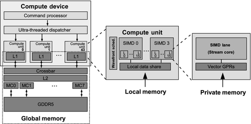
AMD’s OpenCL implementation is designed to run on both x86 CPUs and AMD GPUs in an integrated manner. All host code executes as would be expected on the general-purpose x86 CPUs in a machine, along with operating system and general application code. However, AMD’s OpenCL implementation is also capable of compiling and executing OpenCL C code on x86 devices using the queuing mechanisms provided by the OpenCL runtime. Figure 8.1 shows a diagram of an AMD FX-8350 CPU, which will be used to illustrate the mapping of OpenCL onto an x86 CPU.
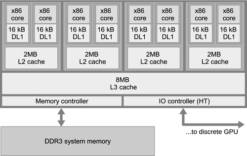
The entire chip in Figure 8.1 is consumed by the OpenCL runtime as a single device that is obtained using clGetDeviceIDs(). The device is then passed to API calls such as clCreateContext(), clCreateCommandQueue(), and clBuildProgram(). The CPU device requires the CL_DEVIce:TYPE_CPU flag (or CL_DEVIce:TYPE_ALL flag) to be passed to the device types parameter of clGetDeviceIDs().
Within the CPU, OpenCL can run on each of the eight cores. If the entire CPU is treated as a single device, parallel workloads can be spread across the CPU cores from a single queue, efficiently using the parallelism present in the system. It is possible to split the CPU into multiple devices using the device fission extension.
8.1.1 Runtime Implementation
The OpenCL CPU runtime creates a thread to execute on each core of the CPU (i.e., a worker pool of threads) to process OpenCL kernels as they are generated. These threads are passed work by a core management thread for each queue that has the role of removing the first entry from the queue and setting up work for the worker threads. Any given OpenCL kernel may comprise thousands of work-groups, for which arguments must be appropriately prepared, and memory must be allocated and possibly initialized.
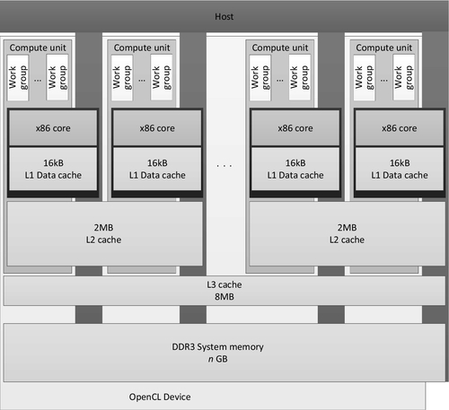
OpenCL utilizes barriers and fences to support fine-grained synchronization. On a typical CPU-based system, in which the operating system is responsible for managing interthread communication, the cost of interacting with the operating system is a barrier to achieving efficient scaling of parallel implementations. In addition, running a single work-group across multiple cores could create cache-sharing issues. To alleviate these issues, the OpenCL CPU runtime executes a work-group within a single operating system thread. The OpenCL thread will run each work-item in the work-group in turn before moving on to the next work-item. After all work-items in the work-group have finished executing, the worker thread will move on to the next work-group in its work queue. As such, there is no parallelism between multiple work-items within a work-group, although between work-groups multiple operating system threads allow parallel execution when possible. Given this approach to scheduling work-groups, a diagram of the mapping of OpenCL to the FX-8350 CPU is shown in Figure 8.2.
In the presence of barrier synchronization, OpenCL work-items within a single work-group execute concurrently. Each work-item in the group must complete the section of the code that precedes the barrier operation, wait for other work-items to reach the barrier, and then continue execution. At the barrier operation, one work-item must terminate and another continue; however, it is impractical for performance reasons to let the operating system handle this with thread preemption (i.e., interrupting one thread to allow another to run). Indeed, as the entire work-group is running within a single thread, preemption would have no effect. In AMD’s OpenCL CPU runtime, barrier operations are supported using setjmp and longjmp. The setjmp call stores the system state and longjmp restores it by returning to the system state at the point where setjmp was called [1]. The runtime provides custom versions of these two functions because they need to work in cooperation with the hardware branch predictor and maintain proper program stack alignment. Figure 8.3 shows the execution flow of work-groups by CPU threads.
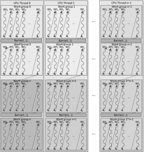
Note that although a CPU thread eventually executes multiple work-groups, it will complete one work-group at a time before moving on to the next. When a barrier is involved, it will execute every work-item of that group up to the barrier, then every work-item after the barrier, hence providing correct barrier semantics and reestablishing concurrency—if not parallelism—between work-items in a single work-group.
Work-item data stored in registers are backed into a work-item stack in main memory during the setjmp call. This memory is carefully laid out to behave well in the cache, reducing cache contention and hence conflict misses and improving the utilization of the cache hierarchy. In particular, the work-item stack data is staggered in memory to reduce the chance of conflicts, and data is maintained in large pages to ensure contiguous mapping to physical memory and to reduce pressure on the CPU’s translation lookaside buffer.
8.1.2 Vectorizing Within a Work-Item
The AMD Piledriver microarchitecture includes 128-bit vector registers and operations from various Streaming SIMD Extensions (SSE) and Advanced Vector Extensions (AVX) versions. OpenCL C includes a set of vector types: float2, float4, int4, and other data formats. Mathematical operations are overloaded on these vector types, enabling the following operations:
These vector types are stored in vector registers, and operations on them compile to SSE and AVX instructions on the AMD Piledriver architecture. This offers an important performance optimization. Vector load and store operations, as we also see in our low-level code discussions, improve the efficiency of memory operations. Currently, access to single instruction, multiple data (SIMD) vectors are entirely explicit within a single work-item: we will see how this model differs on AMD GPU devices when we discuss a GPU in Section 8.2.
8.1.3 Local Memory
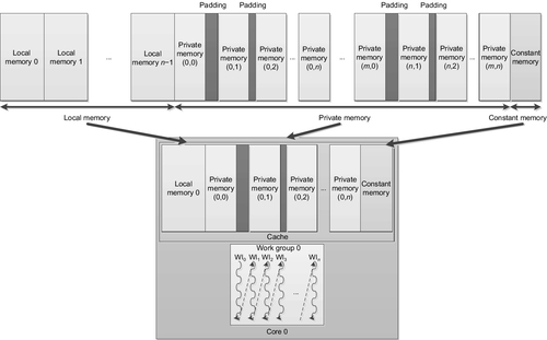
The AMD Piledriver design does not provide dedicated hardware for scratchpad memory buffers. CPUs typically provide multiple levels of memory caching in order to hide main memory access latency. The data localization provided by local memory supports efficient mapping onto the CPU cache hierarchy and allows the kernel developer to improve cache performance even in the absence of a true hardware scratchpad. To improve cache locality, local memory regions are allocated as an array per CPU thread and are reused for each work-group executed by that thread. For a sequence of work-groups, barring any data races or memory conflicts, there is then no need for this local memory to generate further cache misses. As an additional benefit, there is no overhead from repeated calls to memory allocation routines. Figure 8.4 shows how we would map local memory to the AMD CPU cache.
Despite the potential advantages of the use of local memory on the CPU, it can also have a negative impact on performance for some applications. If a kernel is written such that its data accesses have good locality (e.g., a blocked matrix multiplication), then using local memory as storage will effectively perform an unnecessary copying of data while increasing the amount of data that needs to fit in the level 1 (L1) cache. In this scenario, performance can possibly be degraded from smaller effective cache size, unnecessary cache evictions from the added contention, and the data copying overhead.
8.2 OpenCL on the AMD Radeon R9 290X GPU
In this section, we will use the term “wavefront” when referring to hardware threads running on AMD GPUs (also called “warp” by NVIDIA). This helps avoid confusion with software threads—work-items in OpenCL and threads in CUDA. However, sometimes use of the term “thread” is unavoidable (e.g., multithreading) or preferable when describing GPU characteristics in general. In this context, we will always use “threads” when referring to hardware threads. Although this section includes many specifics regarding the Radeon R9 290X GPU, the approach of mapping work-items to hardware threads, scheduling and occupancy considerations, and the layout of the memory system are largely similar across device families and between vendors.
A GPU is a significantly different target for OpenCL code compared with the CPU. The reader must remember that a graphics processor is primarily designed to render three-dimensional graphics efficiently. This goal leads to significantly different prioritization of resources, and thus a significantly different architecture from that of the CPU. On current GPUs, this difference comes down to a few main features, of which the following three were discussed in Chapter 2:
1. Wide SIMD execution: A far larger number of execution units execute the same instruction on different data items.
2. Heavy multithreading: Support for a large number of concurrent thread contexts on a given GPU compute core.
3. Hardware scratchpad memory: Physical memory buffers purely under the programmer’s control.
The following are additional differences that are more subtle, but that nevertheless create opportunities to provide improvements in terms of latency of work dispatch and communication:
• Hardware synchronization support: Supporting fine-grained communication between concurrent threads.
• Hardware managed tasking and dispatch: Work queue management and load balancing in hardware.
Hardware synchronization support reduces the overhead of synchronizing execution of multiple wavefronts on a given compute unit, enabling fine-grained communication at low cost.
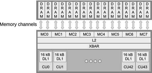
GPUs provide extensive hardware support for task dispatch because of their deep roots in the three-dimensional graphics world. Gaming workloads involve managing complicated task graphs arising from interleaving of work in a graphics pipeline. As shown in the high-level diagram of the AMD Radeon R9 290X in Figure 8.5, the architecture consists of a command processor and work-group generator at the front that passes constructed work-groups to hardware schedulers. These schedulers arrange compute workloads onto the 44 cores spread throughout the device. The details of each compute unit are described in Section 8.2.2.
To obtain the high degree of performance acceleration associated with GPU computing, scheduling must be very efficient. For graphics, wavefront scheduling overhead needs to remain low because the chunks of work may be very small (e.g., a single triangle consisting of a few pixels). Therefore, when writing kernels that we want to achieve high performance on a GPU, we need to
• provide a lot of work for each kernel dispatch;
• batch multiple launches together if kernels are small.
By providing a sufficient amount of work in each kernel, we ensure that the work-group generation pipeline is kept occupied so that it always has more work to give to the schedulers and the schedulers always have more work to push onto the SIMD units. In essence, we wish to create a large number of wavefronts to occupy the GPU since it is a throughput machine.
The second point refers to OpenCL’s queuing mechanism. When the OpenCL runtime chooses to process work in the work queue associated with the device, it scans through the tasks in the queue with the aim of selecting an appropriately large chunk to process. From this set of tasks, it constructs a command buffer of work for the GPU in a language understood by the command processor at the front of the GPU’s pipeline. This process consists in (1) constructing a queue, (2) placing it somewhere in memory, (3) telling the device where it is, and (4) asking the device to process it. Such a sequence of operations takes time, incurring a relatively high latency for a single block of work. In particular, as the GPU runs behind a driver running in kernel space, this process requires a number of context switches into and out of kernel space to allow the GPU to start running. As in the case of the CPU, where context switches between short-running threads becomes a significant overhead, switching into kernel mode and preparing queues for overly small units of work is inefficient. There is a fairly constant overhead for dispatching a work queue and further overhead for processing depending on the amount of work in it. This overhead must be overcome by providing very large kernel launches, or long sequences of kernels. In either case, the goal is to increase the amount of work performed for each instance of queue processing.
8.2.1 Threading and the Memory System
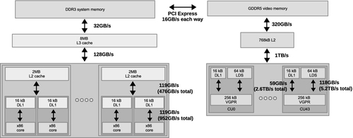
A CPU cache hierarchy is arranged to reduce latency of a single memory access stream: any significant latency will cause that stream to stall and reduce execution efficiency. Alternatively, because the GPU cores use threading and wide SIMD units to maximize throughput at the cost of latency, the memory system is designed to maximize bandwidth to satisfy that throughput, with some latency cost. Figure 8.6 shows an approximation of the memory hierarchy for a system containing an FX-8350 CPU and a Radeon R9 290X GPU.
With relevance to the memory system, GPUs can be characterized by the following:
• A large number of registers.
• Software-managed scratchpad memory called local data shares (LDS) on AMD hardware.
• A high level of on-chip multithreading.
• A single level 2 (L2) cache.
• High-bandwidth memory.
As mentioned previously, graphics workloads fundamentally differ from compute workloads, and have led to the current GPU execution and memory models. Fundamentally, the GPU relies much less heavily on data reuse than does the CPU, and thus has much smaller caches. Even though the size of the L1 data caches are similar between x86 cores and Radeon R9 290X compute units, up to 40 wavefronts execute concurrently on a compute unit, providing a much smaller effective cache size per wavefront. The lack of reliance on caching is based on a number of factors, including less temporal reuse of data in graphics, and owing to the large data sets and amount of multithreading, the inability to realistically cache a working set. When data reuse does occur, multithreading and high-bandwidth memory helps overcome the lack of cache.
Also of note in the memory system is that there is a single, multibanked L2 cache, which must supply data to all compute units. This single-L2-cache design allows the GPU to provide coherence between caches by writing through the L1 caches and invalidating any data that may potentially be modified by another cache. The write-through design makes register spilling undesirable, as every access would require a long-latency operation and would create congestion at the L2 cache.
To avoid spilling, GPUs provide much larger register files than their CPU counterparts. For example, unlike the x86 architecture, which has a limited number of general-purpose registers (16 architectural registers per thread context), the Radeon R9 290X allows a single wavefront to utilize up to 16,384 registers! Wavefronts try to compute using only registers and LDS for as long as possible, and try to avoid generating traffic for the memory system whenever possible.
LDS allows high-bandwidth and low-latency programmer-controlled read/write access. This form of programmable data reuse is less wasteful and also more area/power efficient than hardware-controlled caching. The reduced waste data (data that are loaded into the cache but not used) access means that the LDS can have a smaller capacity than an equivalent cache. In addition, the reduced need for control logic and tag structures results in a smaller area per unit capacity.
Hardware-controlled multithreading in the GPU cores allows the hardware to cover latency to memory. To reach high levels of performance and utilization, a sufficiently large number of wavefronts must be running. Four or more wavefronts per SIMD unit or 16 per compute unit may be necessary in many applications. Each SIMD unit can maintain up to 10 wavefronts, with 40 active across the compute unit. To enable fast switching, wavefront state is maintained in registers, not cache. Each wavefront in flight is consuming resources, and as a result increasing the number of live wavefronts to cover latency must be balanced against register and LDS use.
To reduce the number of requests generated by each wavefront, the caches that are present in the system provide a filtering mechanism to combine complicated gathered read and scattered write access patterns in vector memory operations into the largest possible units—this technique is referred to as coalescing. The large vector reads that result from well-structured memory accesses are far more efficient for a DRAM-based system, requiring less temporal caching than the time-distributed smaller reads arising from the most general CPU code.
Figure 8.6 shows the PCI Express bus as the connection between the CPU and GPU devices. All traffic between the CPU, and hence main memory, and the GPU must go through this pipe. Because PCI Express bandwidth is significantly lower than access to DRAM and even lower than the capabilities of on-chip buffers, this can become a significant bottleneck on a heavily communication-dependent application. In an OpenCL application, we need to minimize the number and size of memory copy operations relative to the kernels we enqueue. It is difficult to achieve good performance in an application that is expected to run on a discrete GPU if that application has a tight feedback loop involving copying data back and forth across the PCI Express bus.
8.2.2 Instruction Set Architecture and Execution Units
A simplified version of a Radeon R9 290X compute unit based on AMD’s Graphics Core Next (GCN) architecture is shown in Figure 8.7. Compute units in the Radeon R9 290X have four SIMD units. When a wavefront is created, it is assigned to a single SIMD unit within the compute unit (owing to register allocation) and is also allotted the amount of memory it requires within the LDS. As wavefronts contain 64 work-items and the SIMD unit contains 16 lanes, vector instructions executed by a wavefront are issued to the SIMD unit over four cycles. Each cycle, wavefronts belonging to one SIMD unit are selected for scheduling. This way, every four cycles, a new instruction can be issued to the SIMD unit, exactly when the previous instruction is fully submitted to the pipeline.
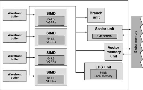
Recall that within a compute unit, the Radeon R9 290X has a number of additional execution units in addition to the SIMD unit. To generate additional instruction-level parallelism (ILP), the Radeon R9 290X compute unit looks at the wavefronts that did not schedule an instruction to the SIMD, and considers them for scheduling instructions to the other hardware units. In total, the scheduler may select up to five instructions on each cycle onto one of the SIMD units, the scalar unit, memory unit, LDS, or other hardware special function devices [2]. These other units have scheduling requirements different from those of the SIMD units. The scalar unit, for example, executes a single instruction for the entire wavefront and is designed to take a new instruction every cycle.
In previous devices, such as the Radeon HD 6970 architecture presented in Chapter 2, control flow was managed automatically by a branch unit. This design led to a very specialized execution engine that looked somewhat different from other vector architectures on the market. The Radeon R9 290X design is more explicit in integrating scalar and vector code instruction-by-instruction, much as an x86 CPU will when integrating SSE or AVX operations. Recall that each wavefront (64 work-items) executes a single instruction stream (i.e., a single program counter is used for all 64 work-items), and that all branching is performed at wavefront granularity. In order to support divergent control flow on the Radeon R9 290X, the architecture provides an execution mask used to enable or disable individual results from being written. Thus, any divergent branching between work-items in a wavefront requires restriction of instruction set architecture (ISA) to a sequence of mask and unmask operations. The result is a very explicit sequence of instruction blocks that execute until all necessary paths have been covered. Such execution divergence creates inefficiency as only part of the vector unit is active at any given time. However, being able to support such control flow improves the programmability by removing the need for the programmer to manually vectorize code. Very similar issues arise when developing code for competing architectures, such as NVIDIA’s GeForce GTX 780, and are inherent in software production for wide-vector architectures, whether manually, compiler, or hardware vectorized, or somewhere in between.
The following is an example of code designed to run on the Radeon R9 290X compute unit (see the Radeon R9 290X family Sea Islands series ISA specification; [3]). Let us take a very simple kernel that will diverge on a wavefront of any width greater than one:
While this is a trivial kernel, it will allow us to see how the compiler maps this to ISA, and indirectly how that ISA will behave on the hardware. When we compile this for the Radeon R9 290X, we get the following:
This code may be viewed, like OpenCL code, as representing a single lane of execution: a single work-item. However, unlike the higher-level language, here we see a combination of scalar operations (prefixed with s_), intended to execute on the scalar unit of the GPU core in Figure 8.7, and vector operations (prefixed with v_) that execute across one of the vector units.
If we look at Line 11 of Listing 8.1, we see a vector comparison operation that tests the work-item ID (stored in v0) against the constant 0 for each work-item in the wavefront. The result of the operation is stored as a 64-bit Boolean bitmask in two consecutive scalar registers (s[4:5]). The resulting bitmask will be used to determine which work-items will execute each conditional path in the OpenCL C kernel.
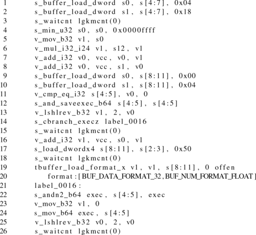
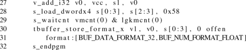
Next, Line 12 implicitly manipulates the execution mask by ANDing the current execution mask with the comparison bitmask. In this case, the resulting execution mask will be used to compute the if clause of the conditional. The previous execution mask is stored in the destination scalar registers (in this example, s[4:5], which previously held the comparison bitmask, now holds the previous execution mask). The previous execution mask will be used when determining which work-items will execute the else clause of the conditional and will also be used again to reset the execution mask after the conditional completes. Additionally, this operation ensures that the scalar condition code (SCC) register is set: this is what will trigger the conditional branch.
Setting the SCC register is an optimization, which allows an entire branch of the conditional to be skipped if it has been determined that no work-items will enter it (in this case, if the bitmask is zero, the s_cbranch_execz instruction on Line 14 could potentially allow the if conditional clause to be skipped). If the conditional branch does not happen, the code will enter the else clause of the conditional. In the current example, work-item 0 will generate a 1 for its entry of the bitmask, so the if conditional will be executed—just by a single SIMD lane (starting on Line 16).
When the if clause is executed, a vector load (a load from the tbuffer or texture buffer, showing the graphics heritage of the ISA) on Line 19 pulls the expected data into a vector register, v1. Line 19 is the last operation for the if clause. Note that while the original OpenCL C code also had a store following the load, the compiler factored out the store to later in the program in the compiled code.
Next, Line 22 takes the original execution mask and ANDs it with the bitwise-negated version of the current execution mask. The result is that the new execution mask represents the set of work-items that should execute the else clause of the conditional. Instead of loading a value from memory, these work-items move the constant value 0 into v1 on Line 23. Notice that the values to be stored to memory from both control flow paths are now stored in the v1 register. This will allow us to execute a single store instruction later in the program.
Attentive readers may have noticed that there is no branch to skip the else clause of the conditional in the program listing. In this case, the compiler has decided that, as there is no load to perform in the else branch, the overhead of simply masking out the operations and treating the entire section as predicated execution is an efficient solution, such that the else branch will always execute and may simply not update v1.
Obviously this is a very simple example. With deeply nested conditionals, the mask code can be complicated with long sequences of storing masks and ANDing with new condition codes, narrowing the set of executing lanes at each stage until finally scalar branches are needed. At each stage of narrowing, efficiency of execution decreases, and as a result, well-structured code that executes the same instruction across the vector is vital for efficient use of the architecture. It is the sophisticated set of mask management routines and other vector operations that differentiates this ISA from a CPU ISA such as SSE, not an abstract notion of having many more cores.
Finally, on Line 24, the execution mask is reset to its state before diverging across the conditional, and the data currently stored in v1 are written out to memory using the tbuffer store instruction on Line 30.
8.2.3 Resource Allocation
Each SIMD unit on the GPU includes a fixed amount of register and LDS storage space. There is 256 kB of registers on each compute unit. These registers are split into four banks such that there are 256 registers per SIMD unit, each 64 lanes wide and 32 bits per lane. These registers are divided on the basis of the number of wavefronts executing on the compute unit. There is 64 kB of LDS on each compute unit, accessible as a random-access 32-bank SRAM. The LDS is divided between the number of work-groups executing on the compute unit, on the basis of the local memory allocation requests made within the kernel and through the OpenCL runtime parameter-passing mechanism.
When executing a single kernel on each compute unit, as is the standard mapping when running an OpenCL program, we might see a resource bottleneck, as seen in Figure 8.8. In this diagram, we see two work-groups each containing two wavefronts, where each work-item (and hence wavefront scaled up) needs 42 vector registers and a share in 50 scalar registers, and the work-group needs 24 kB of LDS. This allocation of four wavefronts per compute unit is limited by the LDS requirements of the work-group and is below the minimum number of wavefronts we need to run on the device to keep the device busy, as with only one wavefront per SIMD unit we have no capacity to switch in a replacement when the wavefront is executing scalar code or memory operations. A general expression for determining the work-group occupancy on a compute unit within the Radeon R9 290X is given in Equation 8.1:

In Equation 8.1, VGPR is vector general purpose register, SGPR is scalar general purpose register, WI is work-item, WG is work-group, and WF is wavefront. The parameters based on the compiled OpenCL kernel are those shown in bold.
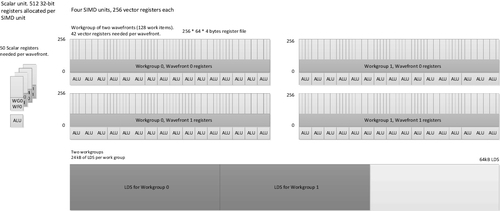
In the example in Figure 8.8, if we can increase the number of wavefronts running on the SIMD unit (empirically four or more wavefronts), we have a better chance of keeping the scalar and vector units busy during control flow and, particularly, memory latency, where the more wavefronts running, the better our latency hiding. Because we are LDS limited in this case, increasing the number of wavefronts per work-group to three would be a good start if this is practical for the algorithm. Alternatively, reducing the LDS allocation would allow us to run a third work-group on each compute unit, which is very useful if one wavefront is waiting for barriers or memory accesses and hence not for the SIMD unit at the time.
Each wavefront runs on a single SIMD unit and stays there until completion. Any set of wavefronts that are part of the same work-group stay together on a single compute unit. The reason for this should be clear when we see the amount of state storage required by each group: in this case, we see 24 kB of LDS and just over 21 kB of registers per work-group. This would be a significant amount of data to have to flush to memory and move to another core. As a result, when the memory controller is performing a high-latency read or write operation, if there is not another wavefront with arithmetic logic unit (ALU) work to perform ready to be scheduled onto the SIMD unit, hardware will lie idle.
8.3 Memory Performance Considerations in OpenCL
8.3.1 Global Memory
Issues related to memory in terms of temporal and spatial locality were discussed in Chapter 2. Obtaining peak performance from an OpenCL program depends heavily on utilizing memory efficiently. Unfortunately, efficient memory access is highly dependent on the particular device on which the OpenCL program is running. Access patterns that may be efficient on the GPU may be inefficient when run on a CPU. Even when we move an OpenCL program to GPUs from different manufacturers, we can see substantial differences. However, there are common practices that will produce code that performs well across multiple devices.
In all cases, a useful way to start analyzing memory performance is to judge what level of throughput a kernel is achieving. A simple way to do this is to calculate the memory bandwidth of the kernel:
where EB is the effective bandwidth, Br is the number of bytes read from global memory, Bw is the number of bytes written to global memory, and t is the time required to run the kernel.
The time, t, can be measured using profiling tools such as the AMD CodeXL Profiler. Br and Bw can often be calculated by multiplying the number of bytes each work-item reads or writes by the global number of work-items. Of course, in some cases, this number must be estimated because we may branch in a data-dependent manner around reads and writes.
Once we know the bandwidth measurement, we can compare it with the peak bandwidth of the execution device and determine how far away we are from peak performance: The closer to the peak, the more efficiently we are using the memory system. If our numbers are far from the peak, then we can consider restructuring the memory access pattern to improve utilization.
Spatial locality is an important consideration for OpenCL memory access. Most architectures on which OpenCL runs are vector based at some level (whether SSE-like vector instructions or automatically vectorized from a lane-oriented input language such as AMD IL or NVIDIA PTX), and their memory systems benefit from issuing accesses together across this vector. In addition, localized accesses offer caching benefits.
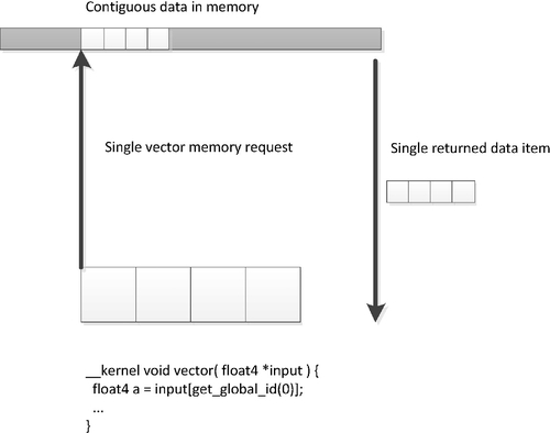
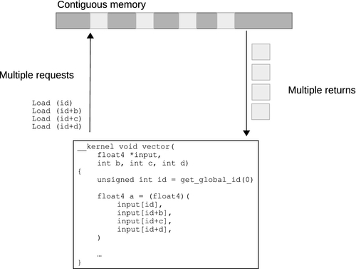
There is a vector instruction set on most modern CPUs; the various versions of SSE and the AVX are good examples. For efficient memory access, we want to design code such that full, aligned, vector reads are possible using these instruction sets. Given the small vector size, the most efficient way to perform such vector reads is to give the compiler as much information as possible by using vector data types such as float4. Such accesses make good use of cache lines, moving data between the cache and registers as efficiently as possible. However, on these CPUs, caching helps cover some of the performance loss from performing smaller, unaligned, or more randomly addressed reads. Figures 8.9 and 8.10 provide a simple example of the difference between a single contiguous read and a set of four random reads. Not only do the narrower reads hit multiple cache lines (creating more cache misses if they do not hit in the cache), but they also cause less efficient transfers to be passed through the memory system.
GPU memory architectures differ significantly from CPU memory architectures, as discussed in Chapter 2 and earlier in this chapter. GPUs use multithreading to cover some level of memory latency, and are biased in favor of ALU capability rather than caching and sophisticated out-of-order logic. Given the large amount of compute resources available on typical GPUs, it becomes increasingly important to provide high bandwidth to the memory system if we do not want to starve the GPU. Many modern GPU architectures, particularly high-performance desktop versions such as the latest AMD Radeon and NVIDIA GeForce designs, utilize a wide SIMD architecture. Imagine the loss of efficiency if Figure 8.10 scaled to a 64-wide hardware vector, as we see in the AMD Radeon R9 architecture.
Efficient access patterns differ even among these architectures. For an x86 CPU with SSE, we would want to use 128-bit float4 accesses, and we would want as many accesses as possible to fall within cache lines to reduce the number of cache misses. For the AMD Radeon R9 290X GPU architecture, consecutive work-items in a wavefront will issue a memory request simultaneously. These requests will be delayed in the memory system if they cannot be efficiently serviced. For peak efficiency, the work-items in a wavefront should issue 32-bit reads such that the reads form a contiguous 256-byte memory region so that the memory system can create a single large memory request. To achieve reasonable portability across different architectures, a good general solution is to compact the memory accesses as effectively as possible, allowing the wide-vector machines (AMD and NVIDIA GPUs) and the narrow vector machines (x86 CPUs) to both use the memory system efficiently. To achieve this, we should access memory across a whole work-group starting with a base address aligned to work-groupSize * loadSize, where loadSize is the size of the load issued by each work-item, and which should be reasonably sized—preferably 32 bits on AMD GCN-based architectures, 128 bits on x86 CPUs and older GPU architectures, and expanding to 256 bits on AVX-supported architectures. The reason that 32-bit accesses are preferable on AMD GCN-based architectures is explained in the following discussion regarding the efficiency of memory requests.
Complications arise when we are dealing with the specifics of different memory systems, such as reducing conflicts on the off-chip links to DRAM. For example, let us consider the way in which the AMD Radeon architecture allocates its addresses. Figure 8.11 shows that the low 8 bits of the address are used to select the byte within the memory bank; this gives us the cache line and subcache line read locality. If we try to read a column of data from a two-dimensional array, we already know that we are inefficiently using the on-chip buses. It also means that we want multiple groups running on the device simultaneously to access different memory channels and banks. Each memory channel is an on-chip memory controller corresponding to a link to an off-chip memory (Figure 8.12). We want accesses across the device to be spread across as many banks and channels in the memory system as possible, maximizing concurrent data access. However, a vector memory access from a single wavefront that hits multiple memory channels (or banks) occupies those channels, blocking access from other wavefronts and reducing overall memory throughput. Optimally, we want a given wavefront to be contained with a given channel and bank, allowing multiple wavefronts to access multiple channels in parallel. This will allow data to stream in and out of memory efficiently.

To avoid using multiple channels, a single wavefront should access addresses from within a 64-word (256-byte) region, which is achievable if all work-items read 32 bits from consecutive addresses. The worst possible situation is if each work-item in multiple wavefronts reads an address with the same value above bit 8: each one hits the same channel and bank, and accesses are serialized, achieving a small fraction of peak bandwidth. More details on this subject for AMD architectures can be found in AMD’s OpenCL programming guide [4]. Similar information is provided to cover the differences in competing architectures from the respective vendors—for example, NVIDIA’s CUDA programming guide [5].
8.3.2 Local Memory as a Software-Managed Cache
Most OpenCL-supporting devices have some form of cache support. Owing to their graphics-oriented designs, many GPUs have read-only data caches that enable some amount of spatial reuse of data.
The easiest way to guarantee the use of caches on a wide range of devices is to use OpenCL image types (discussed in Chapters 6 and 7). On GPUs, images map data sets to the texture read hardware and, assuming that complicated filtering and two-dimensional access modes are not needed, improve memory efficiency on the GPU. However, GPU caches are small compared with the number of active wavefront contexts reading data. Programmer-controlled scratchpad memory in the local address space is an efficient approach for caching data with less overhead from wasted space than hardware-controlled caches, better power efficiency, and higher performance for a given area. It is also useful as a way to exchange data with other work-items in the same work-group with a very low and, barring collisions, guaranteed access latency. Figure 5.5 showed a simple example of this approach.
Of course, there are trade-offs when considering how best to optimize data locality. In some cases, the overhead of the extra copy instructions required to move data into local memory and then back out into the ALU (possibly via registers) will sometimes be less efficient than simply reusing the data out of cache. Moving data into local memory is most useful when there are large numbers of reads and writes reusing the same locations, when the lifetime of a write is very long with a large number of reads using it, or when manual cache blocking offers a way to correct for conflict misses that can often be problematic in two-dimensional data access patterns.
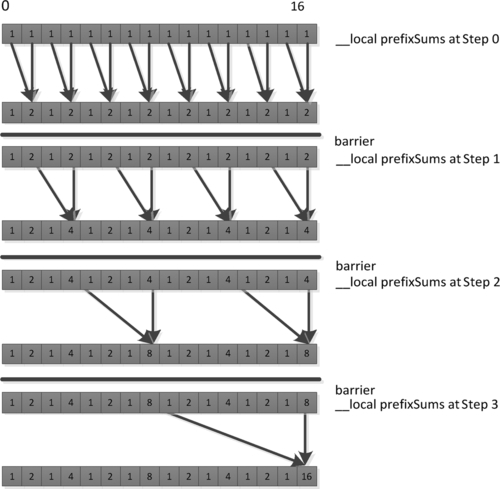
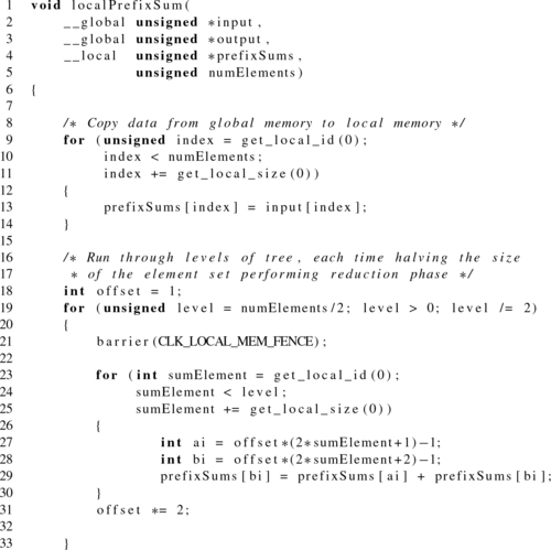
In the case of read/write operations, the benefit of local memory becomes even more obvious, particularly given the wide range of architectures with read-only caches. Consider, for example, the following relatively naive version of a prefix sum code:
Although the previous code is not optimal for many architectures, it does effectively share data between work-items using a local array. The data flow of the first loop (Line 19) is shown in Figure 8.13. Note that each iteration of the loop updates a range of values that a different work-item will need to use on the next iteration. Note also that the number of work-items collaborating on the calculation decreases on each iteration. The inner loop masks excess work-items off to avoid diverging execution across the barrier. To accommodate such behavior, we insert barrier operations to ensure synchronization between the work-items and so that we can guarantee that the data will be ready for the execution of the next iteration.
The prefix sum code in Listing 8.2 uses local memory in a manner that is inefficient on most wide SIMD architectures, such as high-end GPUs. As mentioned in the discussion on global memory, memory systems tend to be banked to allow a large number of access ports without requiring multiple ports at every memory location. As a result, scratchpad memory hardware (and caches, similarly) tends to be built such that each bank can perform multiple reads or concurrent reads and writes (or some other multiaccess configuration), where multiple reads will be spread over multiple banks. This is an important consideration when we are using wide SIMD hardware to access memory. Each cycle, the Radeon R9 290X GPU can process local memory operations from two of the four SIMD units. As each SIMD unit is 16 lanes wide, up to 32 local reads or writes may be issued every cycle to fit with the 32 banks on the LDS. If each bank supports a single access port, then we can achieve this throughput only if all accesses target different memory banks, because each bank can provide only one value. Similar rules arise on competing architectures; NVIDIA’s Fermi architecture, for example, also has a 32-banked local memory.
The problem for local memory is not as acute as that for global memory. In global memory, we saw that widely spread accesses would incur latency because they might cause multiple cache line misses. In local memory, at least on architectures with true scratchpads, the programmer knows when the data is present because he or she put it there manually. The only requirement for optimal performance is that we issue 16 accesses that hit different banks.
Figure 8.14 shows accesses from step 1 of the prefix sum in Figure 8.13 to a simplified eight-bank LDS, where each work-item can perform a single local memory operation per cycle. In this case, our local memory buffer can return up to eight values per cycle from memory. What performance result do we obtain when performing the set of accesses necessary for step 1 of the prefix sum?
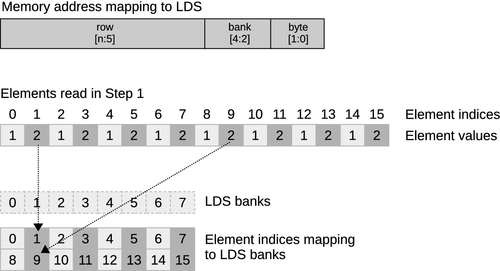
Note that our 16-element local memory (necessary for the prefix sum) is spread over two rows. Each column is a bank, and each row is an address within a bank. Assuming (as is common in many architectures) that each bank is 32 bits wide, and assuming, for simplicity, that the current wavefront is not competing with one from another SIMD unit, our memory address would break down as shown at the top of Figure 8.14. Two consecutive memory words will reside in separate banks. As with global memory, an SIMD vector that accesses consecutive addresses along its length will efficiently access the local memory banks without contention. In Figure 8.13, however, we see a different behavior. Given the second access to local memory, the read from prefixSums[bi] in
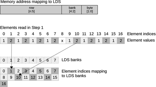
prefixSums[bi] = prefixSums[ai] + prefixSums[bi] on Line 29; tries to read values from locations 3, 7, 11, and 15. As shown in Figure 8.14, 3 and 11 both sit in bank 3, and 7 and 15 both sit in bank 7. There is no possible way to read two rows from the same bank simultaneously, so these accesses will be serialized on GPUs by the hardware, incurring a read delay. For good performance, we might wish to restructure our code to avoid this conflict. One useful technique is to add padding to the addresses, and an example of this is shown in Figure 8.15. By shifting addresses after the first set (aligning to banks), we can change evenly strided accesses to avoid conflicts. Unfortunately, this adds address computation overhead, which can be more severe than the bank conflict overhead; hence, this trade-off is an example of architecture-specific tuning.
Local memory should be carefully rationed. Any device that uses a real scratchpad region that is not hardware managed will have a limited amount of local memory. In the case of the Radeon R9 290X GPU, this space is 64 kB. It is important to note that this 64 kB is shared between all work-groups executing simultaneously on the core. Also, because the GPU is a latency hiding throughput device that utilizes multithreading on each core, the more work-groups that can fit, the better the hardware utilization is likely to be. If each work-group uses 16 kB, then only four can fit on the core. If these work-groups contain a small number of wavefronts (one or two), then there will be barely enough wavefronts to cover latency. Therefore, local memory allocation will need to balance efficiency gains from sharing and efficiency losses from reducing the number of hardware threads to one or two on a multithreaded device.
The OpenCL application programming interface includes calls to query the amount of local memory the device possesses, and this can be used to parameterize kernels before the programmer compiles or dispatches them. The first call in the following code queries the type of the local memory so that it is possible to determine if it is dedicated or in global memory (which may or may not be cached; this can also be queried), and the second call returns the size of each local memory buffer:
8.4 Summary
The aim of this chapter was to show a very specific mapping of OpenCL to an architectural implementation. In this case, it was shown how OpenCL maps slightly differently to a CPU architecture and a GPU architecture. The core principles of this chapter apply to competing CPU and GPU architectures, but significant differences in performance can easily arise from variation in vector width (32 on NVIDIA GPUs, 64 on AMD GPUs, and much smaller on CPUs), variations in thread context management, and instruction scheduling. It is clear that in one book we cannot aim to cover all possible architectures, but by giving one example, we hope that further investigation through vendor documentation will lead to efficient code on whatever OpenCL device is being targeted.