In the previous chapter, you learned about the fundamentals of a drone system and the integral parts of a drone, which are basically hardware, software, and mechanicals. You also learned about the subsystems of the drone and how they map to the features of the drone as a product.
In this chapter, we will primarily discuss the flow of drone system design. The flow will assist you in the deep learning of the system and its applications. Design flow starts with the architecture, which includes all the system elements or blocks, which we will describe in detail in each section on hardware, software, and mechanicals for a quick understanding of the cross-functional engineers and any other team that contributes to the system design.
In this chapter, we’ll focus on the general flow of the system design with annotations relating to the drone system design. We’ll also define, at a high level, what example design we will take for illustration purposes. The details on various stages or steps relating to the specific drone system design will be covered in the upcoming chapters.
System Design
System design, in general, is usually done by a group of experts (or team) involving expertise from hardware, software, and mechanical engineers with different and complementary skill sets. This group of people typically consists of component engineers, CAD engineers, design engineers, test engineers, and program managers. Many times the composition of the team depends upon the nature of the product being designed and developed.
In general, the product design process typically involves three main aspects: specification, architecture, and implementation.
Requirement Specification
Requirement specification is the first step in any system design. The requirement specification step involves gathering the requirements and converting them into detailed document collaterals which act as the starting point for various teams involved in the design. For a complicated electromechanical system like a drone, multiple documents from electrical, mechanical, and software are required to understand the design.
A single source document, which is accountable to generate all of the other architectural documents in sequence or parallel, is the product requirement document (PRD) .
The PRD is the scope of the target system, created with input from the marketing team based on the extensive market research, contributions from the customer, and input from the engineering team. The engineering team works in parallel to gather the requirements and collating the reports and results from feasibility analysis. The PRD can sometimes be interchanged with the system requirement document (SRD) . While different organizations use different terminology, generally PRD is the terminology used by the marketing team, external teams, or non-engineering teams, whereas the term SRD is used by the design team or engineering team.
Architecture
The engineering team generates the engineering specification in response to the PRD, which addresses the possibility of fulfilling the requirements of the PRD or a deviation or alternate way of fulfilling the requirements. There are several other design documents that represent the hardware, software, and mechanicals at a high level to explain the sections to external, cross-functional, and customer teams to keep everybody on the same page before starting the actual design.
Mechanical Design
The mechanical concept is usually done in a CAD (computer-aided design) tool . The output is usually a standard file format that can be opened/imported in any CAD application software or multiple image files showing the sectional view such as top, bottom, and cross-sectional view of the target 3D model concept. Figure 2-1 shows the partially completed or work-in-progress 3D model file developed using CAD tools of an X-frame of a drone. This is not limited to the X-frame; other mechanical parts like enclosures, screws, and propellers need to be designed in the same way to complete the 3D model. The electrical components like the PCB and the interconnects are modeled in a different electrical CAD tool and are imported into a mechanical CAD tool to get the complete 3D concept of the drone. The dimensions and tolerances of the parts need to be more accurate for the 3D model in order to avoid any defect during manufacturing. The mechanical concept is usually a part of the engineering specification and it presents the opportunities and risks of meeting the requirements from the PRD.
Although the perfect balance between hardware, software, and mechanical ingredients is required for an outstanding system design, one of the key selling points for a consumer drone is the aesthetics of the mechanical enclosures. Therefore, a lot of focus is on the mechanical design in the initial phase. Mechanical design, like most other design work, is an iterative process; that means you start with an initial concept and then iterate over it based on feedback. Hardware and software go through the minor changes in the middle or later point of time during the detailed design phase.

A 3D model of the X-frame
The mechanical design process has evolved over last few years with the rise of 3D printing. New consumer-friendly 3D printers can produce dimensional objects. The 3D printers print (create) objects with a plastic-like substance as opposed to traditional printers that spread ink across a page. Building a prototype from the 3D mechanical model is cooler these days, unlike hardware design, which still stay as a longer pole in the system design.
Hardware Design
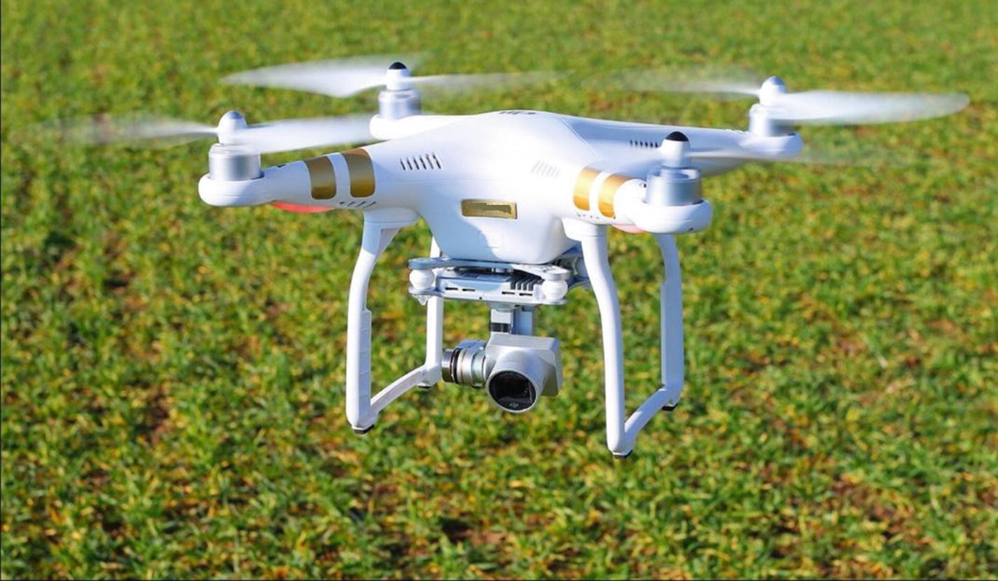
In the past, new product design and development in the field of electronics was by definition hardware design. Today, this isn’t the case; it is only a part of the equation. Hardware design at a concept level or an architectural level is usually explained with an electrical block diagram with all the electrical ingredients interconnected through the compatible electrical interfaces. Generally, all the ingredients are connected to the SOC, which is often considered the brain of the system. A few ingredients can connect to each other directly rather connecting to SOC if the ingredients are independent or the functionality of the specific ingredient demands. The key list of ingredients required for the system also explains the product structure at a high level. Figure 2-2 shows the hardware block diagram, which includes part numbers of the devices used and also completes the key bill of materials of the hardware. These are the minimum required hardware blocks to build a drone; more details in the upcoming chapters.

Drone hardware block diagram and key BOM
Software Design
In a system, the complete functionality is co-provided by hardware (HW) and software (SW). Based on the product PRD, HW and SW partitioning is done. In other words, it shows what part of the functionality is provided by chosen HW blocks and what is covered in SW. After the partition is made, the SW design and development can start straightaway. There are SW design practices and a SW development life cycle that is followed. The focus of this book is not the software design flow since it’s very well established and enough references are available relating to SW product life cycle.
Implementation
This is where the designers narrow their ideas, which can be guaranteed successes, and from there they can outline their plan to make the product. In this phase, the engineers implement the design and build the prototype as per the plan outlined in the previous step. The last stage of this phase is when the product is tested, and from there, improvements are made. The implementation part is explained in detail in upcoming chapters of this book.
Specifications for Our Drone, “Crop Squad”
Drone Hardware Specifications
Subsystems | Features | Specifications |
|---|---|---|
PROCESSING | Quad-core 2.34 GHz | |
MEMORY | RAM | 4 GB |
SD Card 128 GB | ||
uSSD 128 GB | ||
CAMERA | Hyperspectral imaging | Line scan, 600-975nm, >100 bands Interface: USB 3.1 |
AUDIO | Beep, vibration | |
Yes, with stereo speakers(need basis) | ||
COMMS | Wi-Fi 802.11 a/b/g/n/ac, dual-band, | |
4.2, A2DP, LE | ||
Yes, with A-GPS, GLONASS, GALILEO, QZSS | ||
DISPLAY | Yes | |
IO | Type C | Type C USB3.1 for data communication, charging |
SENSORS | Accelerometer, gyro, proximity, compass, barometer | |
OTHERS | FPGA | Flight controllers, embedded controllers, motor PWM controllers |
Mechanical Design
As mentioned in the previous section, defining (creating) or choosing the right mechanical design of the system is the starting point. In the following sections, we will talk about the key aspects of making mechanical design choices.
A drone is not an entirely new concept. The term was used in the early 1900s for UAVs. Different types of drones are already in use for various purposes. Keeping that as a base and the target application in mind, a perfect mechanical design needs to be created that, along with hardware and software, must fulfill all the requirements listed in the PRD.
The simple drone named Crop Squad is designed for agriculture applications and is expected to monitor crops, analyze the local crop health, and upload the reports or upload the raw capture to the datacenter for further analysis. From the mechanical engineering perspective, there are specific things to take care of for this drone.
- 1.
A quadcopter to fly high to cover or get a view of a larger area of the agricultural land
- 2.
A hyperspectral imaging camera to capture the patterns or other observations of the crops (leaves, stems, and pods) periodically
- 3.
A high-speed wireless network to upload the raw image capture back to the datacenter for further processing and analysis or to analyze locally if the drone is equipped with a high computing processor
- 4.
A remote controller to operate the drone from a remote location or equip the drone with artificial intelligence (AI) to do the job independently without any control
At a high level, the requirement looks simple, with four variables: quadcopter, camera, wireless network, and remote. But creating a mechanical design is not as simple as that; numerous variables come into the picture. The mechanical design also depends on the creativity of the individuals. While the form factor or aesthetics of a product (including a drone) are driven by industrial design and marketing, design engineers usually have to apply a lot of creativity and ideas of innovation in meeting the requirements.

Possible mechanical design variants
Definition
The mechanical design is defined as an industrial design (ID) . Mass production can be done only in the factory automation tooling process, because the activity is often a completely repetitive process. This means the design should be predefined as per the manufacturability of factory standards and the factory should be prepared for the manufacturing process for the application-specific ID.
As a part of the ID selection, the choice of materials is important because the factory must be able to handle those materials in the process. For example, the manufacturing process is completely different for metal or plastic, so the factory needs to prepare differently for metal or plastic. An X-frame of the drone can be made from plastic or metal. A plastic part and a metal part need to be designed differently, and the factory process is likely to change based on the material.
With all other things being the same, the ID is one of the key deciding factors since it creates the first impression with the customers, and a favorable impression increases product sales.
Purpose
The PRD lists the high-level applications of the drone. It’s the engineer’s responsibility to learn the next level of details and understand the actual purpose of the drone. For example, Agriculture is the broad area where drones are used for soil and field analysis; to spray the seeds; and to irrigate, monitor, and collect health report of the crops.
If a single drone is designed for all of the above mentioned purpose, the ID and system design will be complex. Even if the system is designed to perform all of these tasks, the design will overload and the system CPU unit may not support multiple parallel activities with the current available technology. Instead, a single drone can be designed to fulfill a combination of two or three applications together. The engineer has to clearly mark the abilities of the drone being built.
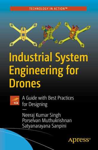
An agriculture drone used to monitor crops
Requirements
Once the purpose is known, the engineer can convert the PRD to next-level detailed mechanical requirements for an ID, including hardware and software.
The PRD and the purpose trigger the engineer’s creativity and give birth to a brand new drone design. The engineer works with a cross-functional team for the materials required, size, and shape of the ID.
The PCBA is considered as a single mechanical part from the hardware team. The dimensions of the PCB are the most important requirements from the hardware engineers to complete an ID. Some other requirements are battery dimension, antenna position, and IO connector placement.

A typical drone system stack-up
- 1.
Propeller: Angled blades attached to the revolving shaft of a motor. These blades gives thrust and are why the drones can fly high.
- 2.
Propeller motor : This is a DC motor attached to the four corners of the X-Frame. Power from the drone’s electrical system rotates the blades to provide thrust to the drone.
- 3.
Enclosure top: A plastic or fiber mechanical enclosure of the drone protects the internal electrical and mechanical subsystems from the external disturbances. Enclosures also provide the aesthetic look for the drone as a product.
- 4.
X-frame: This is the vertebra of the drone. All of the other mechanical parts and subsystems of the drone are attached to the X-frame through different types of fasteners or ties. The X-frame is symmetrical by dimensions and weight on all sides to achieve a balanced flight of the drone. So the cross-sectional view is symmetrical on Y axis.
- 5.
Enclosure bottom: A plastic or fiber mechanical enclosure of the drone protects the internal electrical and mechanical subsystems from the external disturbances. Enclosures also provide the aesthetic look for the drone as a product.
- 6.
Mylar : A form of polyester resin used to make heat-resistant plastic films and sheets. It acts as an insulation layer between the conductive layer of the PCBA and the metallic X-frame.
- 7.
MB ( motherboard ): The PCBA of the system hosts all of the electrical parts of the system soldered on to it. By modifying the PCBA shape, the same layer can accommodate the battery on the sides of the PCBA.
- 8.
CPU: Usually an SOC, it’s the processing unit of the system. All other devices soldered on the PCBA are on the same layer adjacent to the CPU.
- 9.
Shielding and TIM: Digital and RF devices usually need shielding to protect from external disturbances or to protect the external devices through radiation. Radiation from the external world is suppressed by connecting the shield to a system ground.
The TIM, thermal interface materials such as graphite, is pasted as a thin layer on the shield to radiate the excess heat generated from the components of the system.
- 10.
Heat spreader: The heat exchanger that moves heat between a heat source and a secondary heat exchange, whose surface area and geometry are more favorable than the source.
- 11.
Air gap: Provided wherever necessary in a system. This air gap acts an insulator and also accommodates material expansion and contraction due to unavoidable reasons in a system.
- 12.
Camera module : The lower-most part of the drone in this application is the camera module. Attached on the bottom to get a better field of view (FOV) when drone fly high. Most camera modules accommodate ISPs and connect to the SOC through the USB 3.1 interface. If the SOC has integrated ISPs, then the camera sensor can directly connect to the SOC with camera-specific interfaces.
- 13.
DB ( daughterboard ): If all of the ingredients can’t be accommodated in the single PCBA, then there can be several daughterboards on the system to accommodate additional ingredients. Motherboards and daughterboards can be connected through board-to-board interconnections or a flex PCB interconnect. In this drone, the WiFi+BT module cannot be kept below the X-frame. The metal X-frame might obstruct the signal for the module’s embedded antenna. Alternatively, the module can be kept in the same PCBA with the external antenna, which may not be good for an ID.
- 14.
FPC ( flexible PCB ): Generally used to connect one or more rigid PCBs in a complex system.
Dependencies
Although the engineer’s creativity and ideas produce an attractive ID, the discrete components, subsystem location, and other dependencies can limit her ideas from becoming a reality.
Multiple discrete components such as the X-frame, motors, propellers, PCBA, screws, gaskets, enclosures, batteries, FPCs, and cables integrate through various electrical and mechanical interconnects in an ID. Apart from the discrete mechanical components, there are electrical subsystems located on the PCBA, which largely impact the design of the ID.
For example, the position of the power and IO connectors determine the front, back, top, and bottom view of the ID. Usually IO connectors are placed on the back or bottom side of the ID to make them invisible to the user. Also, the presence of wireless components prominently affects the ID design. The antenna is the most vital part of the wireless interface and its placement varies for the mobile network, WiFi, and other RF remote control technologies.
With all of the above mentioned challenges, the mechanical team has to come up with best ID for the product.
Hardware Design
The process of converting the Figure 2-2 block diagram or hardware architecture to a fully functional PCBA is called hardware design. The hardware design fundamentally focuses on getting the desired functionality to the system. PCBA development starts with the hardware requirement capture based on the PRD, followed by ingredients selection and choice of the right PCB to interconnect the ingredients, and finally, the power architecture, design, and implementation for the hardware.
The PCBA is considered as a single discrete mechanical part in an ID. Subsystems and other ingredients of the PCBA are part of the electrical BOM.
Hardware Requirements
The first step in hardware design is the understanding of the hardware requirements. Hardware requirements may vary depending on the operating system and the overall system design, which is usually covered in the PRD.
There are variations possible for a system providing similar functionality. For our case, there could be different variations of drones possible, but still providing the functionality we outlined. The differentiation comes from the parts that are chosen in the system. Generally speaking, there are different modules that can provide certain functionality. However, there may be differences relating to, for example, the power, performance, latency, and durability of those components.
Generally, there are minimum hardware specifications of the devices, which barely meet the requirements. If the system is built with these devices, it’s a low-end product. A low-end product usually lacks speed and quality. So it is the one of the cheapest in the product range or on the market as a whole.
Above minimum requirements, there are recommended specifications for the effective operation of the operating system. Products with these specifications fall in the medium range in terms of cost and quality.
Also, there is a higher end to the hardware specifications of each device, under which the system will operate at high performance. So the product is one of the most expensive or advanced in a product range or on the market as a whole.
Drone Hardware Requirements
Features | Key Component Requirement | Proposals | Dependencies |
|---|---|---|---|
CPU | Quad-core 2.34 GHz | Quad-core 2.34GHz | Required |
Memory | 2GB LPDDR3 | 4GB LPDDR3 | Required |
Storage | 64 GB uSSD | 128GB uSSD | Required |
Camera | 600-975nm, line scan, hyperspectral imaging | 470-900nm, line scan, hyperspectral imaging | Required |
WiFi | 802.11 1x1 ac module | M.2 12*16 802.11 1x1 ac module | Required |
Sensor | Accelerometer, ambient light, gyroscope, temperature, altitude, pressure | Accelerometer, ambient light, gyroscope, temperature, altitude, pressure | Required |
IO ports | 1xUSB Type C 1xuSD4.0 1xuSIM 1xPowerJack | Required | |
Mobile Network | LTE | M.2 LTE Module | Optional |
FPGA | |||
PCB | 12-Layer HDI | 8-Layer HDI | Required |
Power | Integrated | Integrated | Required |
Charger | 7.4V, 5A | 7.4V, 5A | Required |
Battery | 10000mAHr | 10000mAHr | Required |
DC adapter | 12V, 3A | 12V, 3A | Required |
Electrical Ingredients Selection
As explained in Chapter 1, the detailed electrical feature set of the system is directly related to the electrical ingredients of the PCBA. Selection of ingredients is based on the detailed analysis of the current available technologies and anticipated technological developments. Usually, the ingredients supplied by different vendors vary in terms of cost, package, technology, and lead time based on factory production capabilities.
All the ingredients selected should adhere to the technology used in the SOC. The SOC as a central processing unit connects all the ingredients as peripherals of the system. Table 2-1 shows the list of electrical ingredients of the system. The same list will become the key component of the bill of materials, with the addition of the manufacturer and manufacturer part number details.
BOM and Component Procurement
The bill of materials is a list of components required to build a system or product. It includes raw materials, subassemblies, intermediate assemblies, subcomponents, parts, and the quantities of each needed to manufacture an end product. A component may be used for communication between manufacturing partners, or confined to a single manufacturing plant. A bill of materials is often tied to a production order whose issuance may generate reservations for components in the bill of materials that are in stock and requisitions for components that are not in stock.
The list of materials required to build a system or a product is called a system BOM. A system BOM is usually hierarchical in nature with multiple levels. Each component in a BOM or subassembly in the main can be called a child item of the main BOM.
Similarly, the list of components or materials required to build a PCBA is called an electrical BOM (EBOM) . The EBOM is a part of the system BOM in most systems and is one of the child items of the main BOM.
Availability: Availability is usually a development schedule of the part. Design, build date, quantity, and lead time of the part should match the project schedule.
Production status: The production status should be active when the final product is built. Inactive or end-of-life (EOL) samples are recommended for a new design. At the very least, engineering samples should be available during the design phase, if not production samples.
Cost: Cost is a key factor to be negotiated with the manufacturer to get the overall target BOM cost as low as possible.
Operating temperature: Each ingredient falls under different temperature grades like commercial, industrial, and defense. The cost will increase if the operating temperature range increases.
Note
The widely accepted operating temperature range for commercial is – 0 to 60, for industrial is -40 to 85, and for military is -55 to 125.
Storage temperature: The temperature at which devices/products are stored, typically ambient temperature.
All of the parts shown in Figure 2-5 are child items of the system BOM. Reservations should be placed for the parts that need to be procured from the third party-vendors. Custom-built parts like the X-frame, enclosures, head spreader, PCBA, etc. are done at the OEM/ODM factory facility by preparing the factory specific to the drone project.
An OEM (original equipment manufacturer) is a company that manufactures the drone; it is marketed with a different manufacturer’s name.
An ODM (original design manufacturer) is a company that designs and manufactures the product as per the specifications; the product is rebranded by another company for sale.
PCBA Design
The PCBA design is the extended process in the system design. Some degree of pre-work needs to be done during the architecture phase. More details will be explained in the upcoming chapters.
- 1.
PCBA dimensions
- 2.
PCB type
- 3.
PCB layer stack-up
PCBA Dimensions
The target length, width, and thickness of the PCBA are derived from the mechanical design. All of the ingredients need to be accommodated in the given length, width, and height of the PCB. Figure 2-6 illustrates the PCBA dimension.

PCBA dimensions
PCB Type
- 1.
Rigid
- 2.
Flex
- 3.
Hybrid (rigid-flex)
Rigid PCBs are most preferred. Flex PCBs are used in a complex systems where rigid PCBs do not fit.
In the Crop Squad drone, shown in Figure 2-1, the architecture diagram of the SSD and WiFi Bluetooth modules are placed on a separate board and are connected to the main board through a FPC connector. This shows that the electrical part of the drone is split into two rigid PCBAs connected through a flexible PCB. The idea is to keep the WiFi module on a separate PCB to avoid the obstruction of the embedded antenna by the metallic X-frame and to eliminate the need of any external antenna.
In some systems, a rigid PCB breaks into small pieces and is interconnected through the flexible PCBs without any external interconnect, which is also called a hybrid PCB.

Hybrid PCB
Layer Stack-Up
A PCB can be single-sided or double-sided. A single-sided PCB is one that has components placed on one side (top or bottom), whereas a double-sided PCB has components on both the top and bottom side. The advantages of a single-side PCB is low cost manufacturing and easy assembly. No air gap is required for the non-component side inside a mechanical assembly. The manufacturability and assembly cost is high for a double-sided assembly and an air gap is required on both sides in a mechanical assembly, since both sides are mounted with components.
In a complicated system, multiple conductive and dielectric layers are sandwiched and laminated in between. Layer count, copper plane, and dielectric thickness decide the overall thickness of the PCB.
The number of power rails in a system is directly proportional to the power layer count. Signal count, trace width, and density of the high speed and low speed signals determine the signal layer count of the PCB.
The power and signal from different layers are connected through “vias” (drills filled with copper perpendicular to the PCB plane connecting the conductors of the layers). A standard PCB has through hole vias covering the top layer to the bottom layer. An HDI (high-density interconnect) PCB has multiple via structures such as a micro via or a stacked via (connects only two adjacent layers), a buried via (connects internal layers not exposed to any external layers), a blind via (connects the top layer to the next layer under a component) and a through hole via.
PCB stack-up is an important factor in determining the EMC performance of a product. A good stack-up can be very effective in reducing radiation from the loops on the PCB (differential-mode emission), as well as the cables attached to the board (common-mode emission). On the other hand, a poor stack-up can increase the radiation from both of these mechanisms considerably.
Figure 2-8 shows partial layer stack up of 3-6-3+ PCB with buried vias (4-9) connecting 6 internal layers, a through hole via (1-12) connecting all 16 layers, and a micro via or stacked via connecting the adjacent layers for the top 4 and bottom 4 layers. The first column of the table shows the layer name (i.e. signal or power). The signal layer is the layer in which the actual signal with specific impedance is routed. The power layer is made up of one or more copper planes that carry different power supplies for ICs on the PCBA. The second column shows the layer type. The layer type is either a conductive layer with thickness mentioned in ounces along with conductive plating as “1/3oz+plating” or a dielectric layer with material properties mentioned as “PP1067/1078.” The other two columns show the thickness of each layer and tolerance in millimeters. The last column in the stack-up is the dielectric constant of the dielectric materials. In general, the stack-up will have a few more columns, including the trace width of the signal to achieve the target impedances.
A detailed feasibility study needs to be done to select the right PCB layer stack-up. Usually floor planning along with a route study is done with a minimum layer count by the combined effort of electrical design engineers and CAD engineers to arrive the right stack-up.
In Figure 2-2, there are high-speed electrical connections on the PCB such SATA, USB3.1, HDMI, and PCIE. Considering the size of the board and the density of the high-speed signal, the design may require 6 signal layers and 6 power layers based on the initial assessment.
Via arrangements are decided based on the signal and power layer arrangement. In this stack-up, the top 4 and bottom 4 layers can be interconnected though a micro via. The 3-x-3+ mentioned in the stack-up is a micro via on the first and last 3 layers plus an additional layer. Then the center x number of layers are connected though a buried via.

PCB layer stack-up
Floor Plan
SOC, peripheral device, and connector placement
The floor plan also includes the height of the PCB, a major dependency for the mechanical design. Electrical ingredients placed on a PCB vary in height, and the mechanical design needs to account for each and every component. Generally, inductors and capacitors are the tallest electrical components in the PCBA. Also, high-power consumption devices dissipate more heat, and these power dissipating devices need cooling systems. The cooling systems, such as heat sinks and fans, are the non-electrics parts considered part of the PCBA and they add to the overall height of the PCBA.
Power Architecture
The energy consumption and the battery life have become critical system parameters. The early estimation of maximum system power consumption is necessary to design a more efficient power supply.
Battery-operated systems generally have different power states. This power state is more specific to the use cases of drones. Drone system power consumption drastically varies for each power states. Drone system idle is a power state in which all subsystems are on, without any activity. This is a state where the drone is grounded and thus not in the air. Standby is the power state in which the system consumes the lowest possible power. A drone in flight with video recording is the highest power consumption state and it drains the battery at the fastest rate.
Note
System idle, active flight, video recording, sleep, and standby are the different power states a system can support. Not all the power states may be applicable for a system.
The power map is the simple representation of the power architecture. Generally, the power map represents only the maximum power consumption state of the system.
Power Estimation
In any hardware design, the components in the PCBA are broadly classified as active and passive devices. Active devices are the components that consume energy. All ICs are active devices whereas inductors, capacitors, resistors, and diodes are passive devices that do not need any power for operation. ICs such as SOCs and other subsystem devices need more than one power supply (also called a power rail). Generally ICs have a core rail and IO rails, and core rails consume more power than IO rails. More details on the power consumption of the devices are discussed in following chapters.
The power consumption details of each device need to be extracted from the datasheet of the device. The datasheet states the absolute and recommended maximum voltage and current specs of the device for all power states.
In most designs, the number of power rails required for the platform is equal to or more than the required rails of SOC. Considering the SOC and platform requirements are equally complicated and the design demands different power sequencing for the SOC and the platform. Keeping the SOC and platform requirements separate will make the calculation simple.
SOC Power Requirements
Table 2-3 shows the SOC voltage and current requirements. The SOC itself as system on chip with multiple functional unit blocks requires different voltage and current to operate. A typical SOC has functional unit blocks such as core, graphics, memory, clock, PLL, display, camera, high-speed IO, low-speed IO, etc. Each block’s voltage range and current consumption is listed in the table.
Appropriate power devices need to be selected based on the voltage and current requirement. The power supply should meet the voltage tolerance (±5% for 3.3V and ±3% for 1.8V) level mentioned in the datasheet of the each device. The power supply design should accommodate the appropriate filter circuits to eliminate the ripple and noise from the power supply before feeding into the devices. Ripple and noise can be reduced by arranging the power layers in the stack-up as well. Other ways of reducing the ripple are by placing the power components in the right location and implementing the best-known power routing techniques.
SOC Voltage and Current Requirements
SOC Power | 3.3V ±5% | 1.8V ±3% | 1.35V ±3% | 1.2V ±3% | 1.0V ±3% | 0.7−1.1V |
|---|---|---|---|---|---|---|
Core | 3000 | |||||
Graphics | 5000 | |||||
Logic | 1800 | |||||
L2/L3 | 2200 | |||||
Memory | 1200 | |||||
Display IO | 300 | 300 | ||||
CFIO | 500 | 200 | ||||
SDIO | 93 | |||||
USB | 200 | |||||
TOTAL | 593 | 500 | 1200 | 500 | 2200 | 9800 |
Platform Power Requirements
Similar to the SOC, there are multiple other devices on the platform that have different voltage and current requirements. These devices spread across the platform, and the few devices requiring common voltage can be switched on simultaneously without any sequencing. Table 2-4 shows the platform voltage and current requirements.
Multiple subsystems need same the voltage. For example, display, sensors, camera, and modem are different subsystems and require common 3.3V with different current requirements and with no specific sequencing (all the subsystems can be switched on simultaneously).
Platform Voltage and Current Requirements
Subsystem | Ingredients | 5.0V | 3.3V | 1.8V | 1.35V | 1.2V |
|---|---|---|---|---|---|---|
MEMORY | LPDDR3 | 1200 | ||||
STORAGE | uSSD | 300 | ||||
UI | Display, | 100 | ||||
camera, | 900 | |||||
sensors | 10 | 10 | ||||
COMMS | Modem, | 500 | ||||
GPS | 150 | |||||
Wi-Fi/BT, | 400 | |||||
FPGA | FPGA | 500 | ||||
USB | 2.0, 3.0 | 1400 | ||||
TOTAL | 2300 | 1760 | 310 | 0 | 1200 |
Power Devices
The previous section listed the voltage, current, ripple, and noise requirements for the SOC and platform. The total number of voltage rails for the SOC and platform combined and the total calculated current consumption for each rail in the SOC and platform helps the engineer to choose the right power devices for the system. Most power devices fall into two categories: linear and switching regulators.
Linear Regulators
A linear regulator operates by using a voltage-controlled source to force a fixed voltage to appear at the regulator output terminal. The most commonly used linear regulator is the low dropout (LDO) regulator. The difference between the input voltage and the generated output voltage is the dropout voltage. The product of the dropout voltage and the current consumed by the device at the output of the regulator is the power dissipated at the source. Basically, low dropout voltage and less current consumption are the desirable parameters when selecting an LDO.
Switching Regulators
Switching regulators operate by switching on/off a series of devices. A FET will be switched on/off by a pulse width modulation (PWM) controller transferring energy to load. When the switch is on, energy is stored on an inductor and capacitor and is also supplying to load. When the switch is off, the stored energy is discharged to the load until the voltage reaches the minimum required threshold of the load device. The on/off is done in a specific duty cycle to keep the output voltage within the tolerance level of the load device. There are different types of switching regulators: buck, boost, and buck boost regulators.
Choosing the Best Regulator
Comparison of Linear and Switching Reguators
Parameters | Linear | Switching |
|---|---|---|
Function | Only steps down. Input voltage must not be greater than the output voltage. | Step up, step down, and inverts |
Efficiency | Low to medium | High |
Complexity | Low | Medium to high |
Size | Small to medium | Large |
Cost | Low | Medium to high |
Ripple/noise | Low | Medium to high |
Function : Most designs convert high voltage to low voltage. Buck is desirable, and can be either a linear or switching regulator. If any design demands low voltage to high voltage conversion, then the regulator choice is a switching regulator. For example, USB powered systems have 5.0 volts as the main input, but some systems, like displaying black light, need a higher voltage to operate. In this case, a boost regulator is required to up-convert this 5.0 to a higher voltage.
Efficiency: There is no control over the efficiency of the linear regulator. The product of the load current and the difference in the input and output voltage gives the power dissipation of the device. For this reason, linear regulators cannot be used for high load current (the load current limit depends on the dropout voltage and max thermal dissipation of the device). But switching regulators can be used for higher current loads and efficiency can be increased by carefully selecting the external components like low RDS on MOSFETs, low DCR inductors, and low ESR capacitors. For better efficiency, go for switching regulators.
Complexity : A linear regulator is very simple. Less external components are required for stable operation and easy implementation, whereas the switching regulators are complex, due to the external components dependencies. More accurate calculations are required when selecting the components for stable operation.
Size: Linear regulators occupy less space in the board, while switching regulators need more space on the board to accommodate the PWM controller, external MOSFETs, inductors, capacitors, and other analog components.
Cost: The architecture of the linear regulator is simple so the cost is less. The switching regulator cost is high considering its advantages of high current and better efficiency in a complex device architecture. On top of the device cost, the switching regulator needs external components for normal operation, so the overall cost is multiple times higher than that of a linear regulator.
Ripple/noise: Ripple and noise are lower in a linear regulator; this quality makes the linear regulator more suitable for analog designs and clock and PLL blocks in the SOC. Switching regulator outputs are noisier than linear ones even with multistage filters.
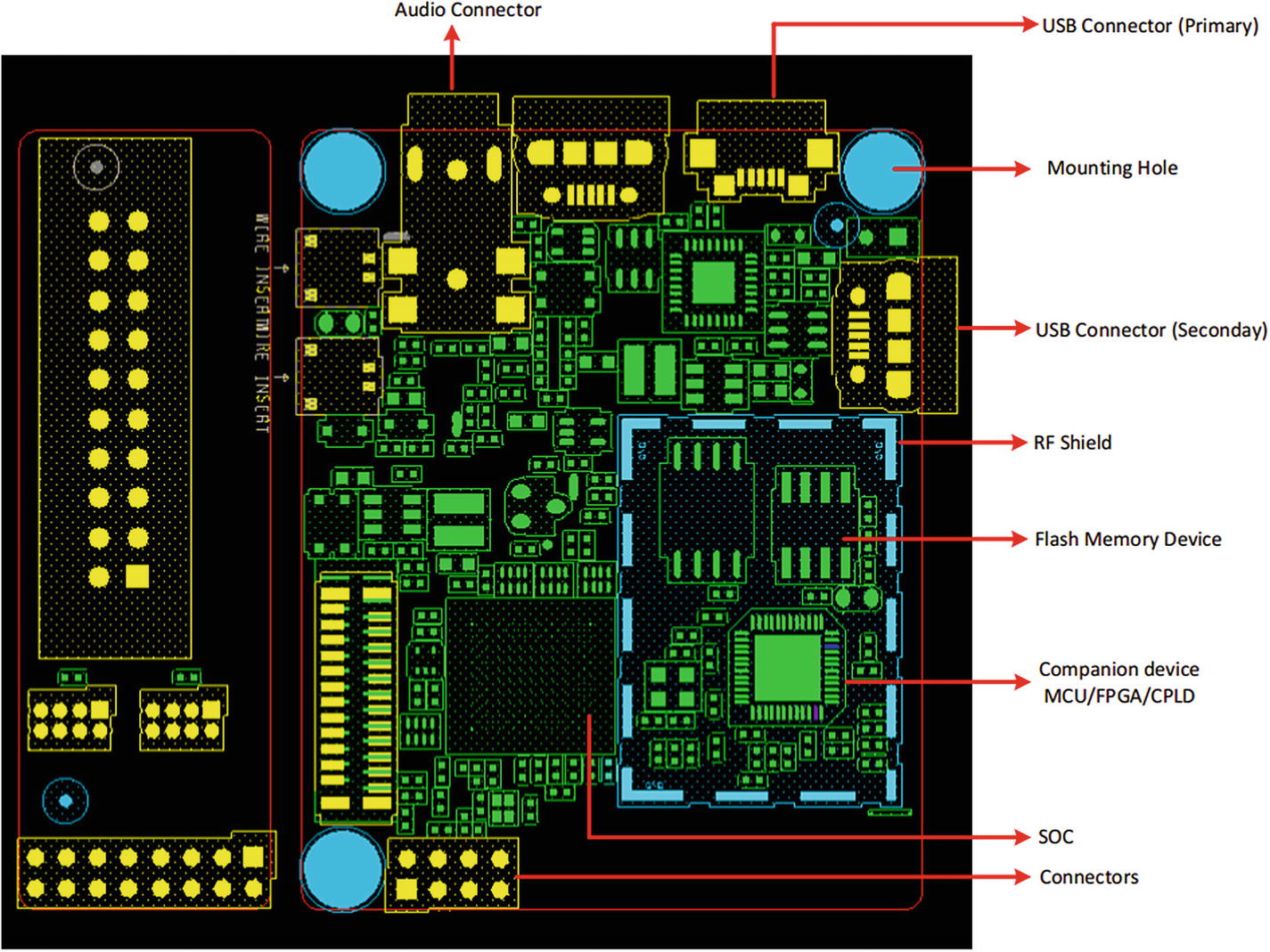
Power Map
The previous section explained the pros and cons of the switching and linear regulators. Linear or switching regulators need to be selected for multiple power rails of the SOC and platform. Among the power rails, some need to be always on and some need to be power-gated whenever the system goes to sleep or the subsystem is inactive for some reason. Also, there are different power sequencing requirements for the SOC, platform, and other devices if specified in the datasheet.
All of the requirements for power consumption, power gating, and sequencing on a power map are drawn for easy understanding and are converted to an actual design of circuits. Figure 2-10 illustrates the power map, which will be converted to power design in schematics and then into a PCBA.
- 1.
Source is the type of regulator used to deliver the power. For example, Buck, Buck1… Buck6 are switching regulators used to deliver higher load currents delivering multiple loads together. ALDO, DLDO, and GPLDO are LDOs delivering lower currents either for single load or multiple loads.
- 2.
Rail Name is the name of the connection used on the board to differentiate from one another. Multiple 3.3V will be delivered from multiple sources to multiple loads. Connections should be used to distinguish names to avoid a short circuit on the PCBA.
- 3.
Voltage is the voltage level or the range the source is delivering.
- 4.
Imax is the maximum load current the device will support or specified by the vendor in the datasheet.
- 5.
Iload is the maximum current the device is actually loaded by the subsystem connected to in the design.
System power map
Power Sequencing
Powering up a circuit on a printed circuit board is too often taken for granted and can cause damage and both destructive and nondestructive latch-up conditions. These problems may not be prominent until volume production begins, when the tolerances of devices and designs are put to the test. This is dangerously late in the process and extremely expensive with respect to time and the delivery of projects and products. Errors found at this stage result in numerous modifications, including PCB layout changes, design alterations, and extra anomalies. With the advent of incorporating many functional blocks into one integrated circuit (IC), this results in supplying these blocks with multiple, sometimes equal, or in many instances, differing voltage supplies. As more and more of these SoC ICs proliferate the marketplace, the need for particular power supply sequencing and power management issues arises. There is usually enough information on device datasheets to guide a designer to a correct power-up sequence for an individual IC. However, some ICs specifically require a well-defined power-up sequence. This is true in the case of many of ICs and is quite common in ones using multiple supplies such as converters (consisting of both analog-to-digital converters (ADCs) and digital-to-analog converters (DACs)), digital signal processors (DSPs), audio/video, radio frequency, and many other mixed signal ICs. Essentially, any IC containing some analog input/output with a digital engine falls into this category, where particular power sequencing may be required. On these ICs, there could be separate analog and digital supplies and some may even have a digital input/output supply, as detailed in specific examples discussed in the following sections. Some of the more common supplies presently are +1.8 V, +2.0 V, +2.5 V, +3.3 V, +5 V, −5 V, +12 V, and −12 V.

SOC power-on sequence
SOC Power Sequencing Numbers
Symbol | Description | Min | Max | Units |
|---|---|---|---|---|
Tvin | +V3P3A stable power after +5PA USB power | 0 | NA | us |
Tvddio | +V1P8A stable power after +3P3A | 100 | NA | us |
Tvdd | +V0P9A stable power after +V1P8A | 100 | 300 | us |
Tclkin | Clock active after +V0P9A stable | 100 | NA | us |
Trst | Host reset assertion after clock | 10 | NA | us |
Trst_Width | Host reset active time | 10 | NA | us |
Tirq | Host interrupt assertion after deassertion of Host rest | 50 | 200 | us |
Battery Estimation
Batteries are energy storage devices that are particularly useful for powering small portable devices like phones, laptops, and entertainment devices as well as mobility devices that travel over the Earth’s surface, through water, and in the air.
Battery Constraints
The batteries used in these applications are engineered to meet the unique design constraints imposed by these different applications. These constraints are covered in the following sections.
Number of Cells or Voltage
The term “battery” refers to a system of one or more cells. A cell represents a particular chemical combination capable of producing a voltage and a current. Different chemical combinations produce different voltages. By combining cells in series, the voltage of a battery pack can be increased as a multiple of the number of cells x the voltage of each cell.
Battery Chemistry
A rechargeable battery is referred to as a storage battery and is usually constructed of one or more secondary cells. Each cell is capable of producing a specific voltage with respect to the electrochemical makeup of the cell. Batteries store energy through changes in their internal chemistry. When a battery is discharged through a load like a circuit or a motor, the internal battery chemistry undergoes a change. When the battery is charged, the chemical change is reversed, and the energy is again stored in the battery. A specific amount of energy can be stored in a battery given the specific battery chemistry, the configuration of the battery, and the battery volume and weight.
Cell Voltage and Battery Packs
For NiCad/NiMH, cell voltage is about 1.2V; for lead acid, it is 2.0V; and for lithium cells, it is on the order of 3.6V. Typically, portable electronic devices are designed to run on 12, 24, 36, or 48 voltages. To create these voltages, a number of cells are connected in series in order to form a battery that has the desired net voltage.
Battery Capacity
Battery capacity is published by the manufacturer as a nominal rating for a given set of discharge conditions. These discharge conditions include rate of discharge (C rate), temperature, and minimum cell voltage. Minimum cell voltage is the lowest voltage to which a cell or battery should be charged. Discharging a cell or a battery below the minimum voltage can reduce or even destroy the battery’s capacity to hold a charge.
Battery performance parameters can include voltage, amp-hour capacity, and C rate (rate of discharge).
The C rate refers to the amount of current the battery can sustain for an hour while remaining within a specified voltage range. For a typical 12 volt battery, this voltage range is between 12 volts and 10.5 volts for the battery to be considered fully charged.
Typical units of battery capacity are expressed as a milliamp-hours or mA*h; for larger batteries, it is amp-hours or A*h. This rating implies the discharge rate in amperes that the battery can be expected to sustain for a period of one hour.
Battery capacity varies with the discharge rate. When you discharge a battery at higher rates, the amp-hour capacity of the battery will be less than the nominal or published capacity.
Battery capacity is measured in amp-hours (Ah). A pack that can deliver 1 amp for 1 hour has a capacity of 1 Ah. The battery capacity is usually given by the manufacturer in amp hours (Ah) or milliamp hours (mAh). Suppose a 15lb drone with four motors draws an average of 4 amps for video recording on the flight. If you fit a 4 Ah battery pack, it can be expected to run for one hour on average.
Watt Hours and Energy Density
There are two different ways of indicating battery capacity: you can use either AHr (ampere hour) or WHr (watt hour) for battery life calculations. And both approaches are used in product designs. The WHr approach is more comprehensible. The watt-hours stored in a battery pack are approximated by multiplying the rated amp-hours by the pack voltage.
Energy density usually refers to the energy in watt hours per unit mass of the battery. The energy available from a given battery can be estimated using the manufacturer’s published data for a given battery pack or cell. The information needed to calculate the energy density can also be obtained through direct battery testing. Battery energy is described in units of watt-hours/kilogram.
Battery Cost
Each battery chemistry requires a specific type of charge and charge regime. Battery chemistries and chargers vary in both initial cost and lifetime costs. Lithium-based batteries present higher initial costs than similar capacity batteries employing other chemistries. However, lithium batteries have high energy densities, long life cycles, and are more readily recyclable than other chemistries. These factors contribute to lower lifetime costs.
There is no answer to the question, “What is the best battery system I can buy?” The answer always depends on the many factors involved in a particular application. Battery systems and chemistries can be cost compared using the relationship cost/watt-hr. Low cost/watt-hr figures can indicate cost-effective energy storage.
This is precisely why designers and engineers need to have skills and knowledge to analyze battery regimes in order to make the best selection for a particular application.
For example, a battery used in a drone must have a high energy-to-weight ratio. This would imply an investigation into lithium battery technology. Battery systems can be expensive. It is therefore necessary to make careful evaluations of the requirements and constraints imposed by a particular application.
Software Architecture
Software is the driver (in a way) of a system. In other words, the hardware provides the capabilities, while the software uses the same, makes it run, and provides the desired functionality. Theoretically speaking, there is always a possibility to design purpose-built hardware(with limited or no software) for a particular usage; however, practically speaking, we need to make design decisions in terms of what functionality should be part of hardware and what should be part of software. These design decisions are made very early in the requirement phase. And, once done, the hardware and software system designs run in parallel. Of course, there is some dependency of SW development (and testing) on HW availability. However, the dependency is mitigated by means of using HW simulators. The simulators are used to provide the functional models of hardware, which can be used to run and validate the software.
- 1.
Firmware components: You know that the firmware components are dependent on and tied to the device they are associated with. The device vendor is responsible for providing production-worthy firmware for the device. In this section, the term “device” also includes the SoC.
- 2.
OS and drivers: The OS component is supplied by the OSV (OS vendors). There are a number of OS flavors and variations that we can choose from. This decision is guided by the OS properties and characteristics. For our example, we’ll use a real-time operating system, since drones are real-time devices. The drivers fall into two categories. The drivers for generic devices based on a certain standard can be part of the OS itself, as an inbox component. However, the drivers for devices with differentiated values and characteristics are provided by the device vendor itself. As the choices relating to hardware devices to be used on the system are made during hardware/software co-design, the driver availability for the OS of our choice is also considered. In certain cases, the device vendor may not have the driver for the OS we want to use. In that case, we might have to either use a different device that provides the same functionality or the device vendor might provide the specification of their device and we might have to write the driver ourselves. It is also possible to influence the device vendor to provide the driver for the OS of our choice; it’s a business decision for the device vendor.
- 3.
Sensing, navigation, and control: This is more custom software that we may have to design and develop on our own. There are drone kits available on the market. If we chose to use a particular drone kit, then this piece is available as part of the kit. However, for a custom solution, we will have write our own sensing, navigation, and control system.
- 4.
Application-specific components: Application-specific components, as the name suggests, are based on the intended usage of the drone. There are plenty of applications we could start with and then customize to meet our purpose.
Logistics and Operations Management
Logistics and operations management is critical to the success of the project, which involves high volume manufacturing. Commercial drones are usually produced in high volumes. Agricultural drones like Crop Squad will be manufactured in lesser volumes, but the process of logistics and operation management will be same when it is built by bigger companies partnering with ODM/OEMs. Logistics and operations management is also referred to as supply chain management, and includes all the operations end to end, from the extraction of raw materials to the manufacturing of the end product. Logistics is the key function in meeting market requirements quickly, flexibly, and without incurring inventory cost. There are representatives from the designers, third-party vendors supplying materials, and the factory to manage the logistics and supply chain.
Operations management tracks the overall project schedule, supply chain, stakeholder management, and coordination of internal teams, third-party vendors, and external customers.
Each party or the company participating in the development of the drone benefits from the success of the product; this is common for all types of products, not just drones.
Board and System Assembly
The supply chain management makes sure that the line items of the system BOM and EBOM will be available on the scheduled date for PCB assembly and system assembly.
Demand BOM
The demand BOM generates reservations for components that are in stock and requisitions for components that are not in stock. Each part has a unique part number. This includes the buy items and make items of the board as well as the system. Buy items are the parts that need to be procured from third-party suppliers; they already have unique manufacturer part numbers. Make items will not have a manufacturer or manufacturer part number because they are custom made in the internal design house.
Production BOM
A production BOM is the final BOM. It is hierarchical in nature and includes all board-level and system-level components, subassemblies, and software required for the final product build.
Exactly two weeks before the PCBA build and system build, the BOM needs to be frozen, after which no parts can be added. The addition of any new component in this phase will cause a delay in the PCBA or product build, which will affect the overall product schedule. Two weeks is not a standard practice; it depends on the lead time of the parts used in the BOM. The lead time of some special parts can be in terms of months. Any part added at the last minute with a month-long lead time will hold the PCBA and system build until that part docks in the factory.
Summary
In this chapter, we quickly skimmed through the overall product system design flow. We also talked about some specific considerations of a drone system. Additionally, we created the high-level definition of the drone system that we plan to design. Overall, the chapter sets the background for the detailed discussion of the drone system design that we will go though in the next chapters.