
In the previous chapter, you explored the key considerations for few of the essential ingredients of a drone. This chapter will explain how the electrical ingredients are put together to develop the hardware for the drone. At a high level, drone development can split into drone hardware development and drone system development. Drone hardware or PCBA development is a critical part of system development. The design or selection of components other than hardware completes the system design.
In any electronics system, the PCBA is considered as one single assembly item, particularly in a drone system, where the mechanical and electrical components play an equal and important role. Even then, hardware is the only item that goes through a complicated design process. Unlike the PCBA, other system-level ingredients are either easily procured or manufactured from dedicated suppliers.
PCBA development starts with the architecture, followed by the electrical ingredients selection, which was discussed in the previous chapters. The architecture and ingredients selections are the documentation part of the hardware development. The actual design requires electrical CAD tool involvement most of the time. The PCBA design process has several steps, which can go in parallel or sequential. The first step of the design is PCBA library development and the final step is getting a complete, functionally working PCBA. To get the final working PCBA, the total development cycle is split into design and validation cycles.
As mentioned earlier, this completed PCBA will be a single mechanical component assembled in a drone system.
PCB Library Development
PCB library development is the important task of PCB design and is a time-consuming task. It’s usually done by highly trained professionals in all aspects of library management from creating library elements through to a complete library management environment. A library is usually managed in a central server or a cloud, which provides access to the components for several boards or projects at the same time.
Libraries are created in a specific file format and stored as individual files. Different tools use different file formats. Libraries created for a specific tool can’t be interchanged with other tools. The electrical component library is a one-time creation process and will stay in the server forever. Each component created or newly added will have unique part identification in the same component library.
The entire library has to comply with the latest design technologies as well as standards such as IPC-7351B to ensure a high-quality library.
Symbol Creation
Library development is nothing but symbol creation for the required electrical components in the system. Two types of symbols are created by any board developers in hardware design. They are logical or schematics symbols and CAD symbols or PCB footprints.
A logical symbol is the visual representation of an electrical ingredient in the schematics. Similarly, a footprint is the visual representation of an electrical ingredient in a PCB layout.
Schematics are the visual representation of an electrical circuit. The completed schematic has all of the required symbols connected to each other with wires (nets) as per the design requirement.
The PCB layout is the visual representation of the actual PCB with all of the required PCB footprints connected to each other with copper traces in a multilayer PCB. The PCB layout is done with dimensions and scales matching the actual PCB and finally fabricated to a physical PCB.
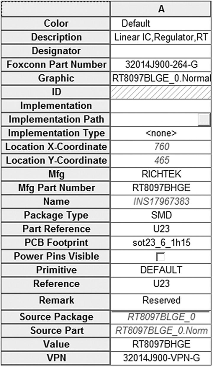
Each individual component in the schematic has an individual logical symbol. One or more logical symbols can use same footprint, if the components share the same package. For example, the logical symbol for resistors is the same for all of the values. The designer has to pick the right value for their design. New resistor values are added to the same logical symbol and are maintained as component libraries whereas complex integrated circuits use unique logical symbols for each component. Technical specifications are added for each component along with other attributes like manufacturer part number and manufacturer name. The footprint is usually added as an attribute for the logical symbol.
Logical Symbol Creation
Every electrical CAD design software/project has a separate librarian tool to create, verify, and manage the component libraries. All symbols are created in a simple 2D plane with simple drawing tools like squares, rectangles, and circles. Discrete components such as resistors, capacitors, inductors, and diodes are created with their unique 2D representation with pins, which is commonly seen in text books. ICs are created as a square or rectangle box with pins attached to it.
A standard practice is to create the symbols with grids. Having grids in the symbols makes the schematic drawing easy; the schematic also should follow a similar grids. Symbols can be created in different styles. Generally, there are guidelines and BKMs (best known methods) to standardize the symbols and schematics for the whole organization.

Logical symbol examples
Symbol Verification
Symbol verification is an important process associated with symbol creation. Once the symbol is created, it needs to be verified by the requested/concerned design engineer before adding it into the central library.
The created symbol should meet the standards and BKMs, and more importantly the symbol should be well-suited for the schematic design. The pins are arranged in such a way that the connections can be done with other peripheral components in a presentable manner and better readability.
So it is crucial to verify that the symbol is created as per the requirement. A symbol cannot be modified once it is added to the central library, which enables other board developers to use the same symbol for other boards and different projects.
PCB Footprint Creation
Similar to logical symbol creation, PCB footprint creation is done with a 2D electrical CAD tool with a simple drawing window. Unlike the logical symbol creation, footprint creation requires a different expertise. A footprint is the exact representation of component pads or a land pattern with proper scale. All footprints are also provided with component height information to generate a 3D view from a layout file if needed.
The footprint is the exact replica of the component pads including dimensions, unlike the logical symbol, which is the only visual representation of the component in a schematic.
A footprint is the visual representation of the component in a PCB layout. The fabricated bare PCB will have all the component pads, exactly created as a footprint on which the components are mounted. This bare PCB with all the components mounted completes the hardware and provides a finished PCBA.

PCB footprint examples
Footprint Verification
Footprint verification is also a critical process, similar to the logical symbol verification. Generally, there are multiple levels of verification done to check the footprint compliance with the IPC guidelines. The footprint is added in the library and accessed by board developers through the component libraries.
Schematics Design
Schematics design is the representation of the detailed electrical circuit elements interconnection within a system. Schematics give a detailed view of the components and the connections between them. It’s the precise low-level design of the hardware block diagram shown in the Figure 4-3.
Every electrical component of the system is placed on the schematic and connected with other components logically and functionally as per the design. Schematics are done considering all the electrical rules, laws, and guidelines for proper operation. Generally, schematic designs are produced by professional analog and deigital electronics design engineers.
Schematics Capture
The drone architecture diagram in Figure 2-2 is converted to a multiple page electrical circuit in a schematics capture. A simple hardware circuit with fewer components can be accommodated on a single page. A complex hardware circuit like a drone can’t be done on a single page. Multiple pages show multiple components connected across the pages. Connections across the pages are always presented with off-page connectors.
All the connections are labelled with net names for easy identification on the layout. Connections without net names are provided with random names and numbers when generating net list. This helps engineers identify and understand the electrical connection and types on a layout tool after importing the schematics files in a layout.
Connections are usually divided into power, ground, and signals. Signals are classified as analog, digital, and RF signals. Digital signals are further classified as high speed and low speed signals. Each connection or interface follows the set of electrical guidelines for connections and terminations. These signal terminations are represented in schematics with appropriate components like resistors, inductors, and capacitors on the actual connection.
In a schematic, each component is provided with a unique reference designator. This reference designator helps to identify the particular component throughout the hardware development especially in layout, bill of materials, testing, and validation.

Schematics example
There are numerous complicated circuit designs for the complete drone hardware, interconnected to each other on multi-page schematics, which may or may not follow the reference circuit from the datasheet.
Design Rules Checking
Design Rules Checking (DRC) is a powerful automated feature that checks both the logical and physical integrity of a design. Checks are made against any or all enabled design rules embedded in the tool. The tool generates reports and suggestions.
This feature should be used on every schematic to show that electrical rules have been maintained and to ensure there are no other design violations. It is particularly recommended that a design rule check always be performed prior to generating the final netlist.
There are also tools available for circuit simulation. Simulation allows the designer to check the circuit operation. However, simulation requires the actual electrical model of the components or the schematic needs to be exported to other simulation tools with all of the electrical specifications of the component.
Generating a Netlist
Netlist generation is the final step in the schematic design. In electronic design, a netlist is a description of the connectivity of an electronic circuit. In its simplest form, a netlist consists of a list of the electronic components in a circuit and a list of the nodes they are connected to. A network (net) is a collection of two or more interconnected components.
The structure, complexity, and representation of a netlist can vary considerably, but the fundamental purpose of every netlist is to convey connectivity information. Netlists usually provide nothing more than instances, nodes, and perhaps some attributes of the components involved.
For the Crop monitoring drone, three different schematics and netlists are generated. One is for the main board, one for the daughterboard, and one for the flex PCB board.
Bill of Materials
The bill of materials (BOM) is a key data set generated from a board design project either from a schematic or a layout tool. This report-type document provides a listing of all components required to build the product, including the bare board, which is essentially the base “component” upon which all other parts are assembled. The BOM acts as a guide for what needs to be procured to build the product as designed. It also provides a means to calculate the cost based on the required number of assembled boards in a requested spin. The BOM is generated through a dedicated and powerful report generation engine, the interface of which is known as the Report Manager from the tool itself.
An electrical BOM can be in a spreadsheet format with attributes in each column. Attributes are usually provided for each component while creating the logical symbol.
The schematics entry tool provides the options to generate the BOM in multiple formats.
Since creating a schematic is a manual, time-consuming process, a BOM is generated frequently from the partially completed schematics. This partial BOM is called an intermediate demand BOM, and it’s sent to the PCBA manufacturing factory. The factory communicates to the suppliers and requests the components and required quantities.
Early submission of the demand BOM is better for long lead components. This enables the supplier to get the required quantities from their side to meet the PCBA manufacturing schedule. Figure 4-4 shows an example of a tool-generated BOM.
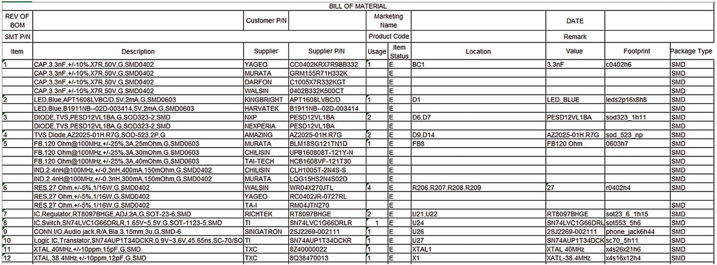
Tool-generated BOM
Symbol Attributes
Symbol attribute window
BOM Generation
A BOM can be generated from the project source documents or from the active PCB document using the Reports > Bill of Materials command from the schematic or PCB editor.
The tool-generated BOM is shared with the PCBA manufacturer to add additional information required for the BOM, usually local supplier and cost data. Being able to cost a project and determine the quantities of design components to be ordered from suppliers/distributors is an essential part of the overall design process.
Supplier: Name of the supplier
Supplier currency: Alphabetic code for the chosen currency used for pricing data. Usually US dollars for most suppliers.
Supplier order quantity: Number of units required to fulfill the desired production quantity of the product.
Supplier part number: Part number for the supplier item. This is different from the manufacturing part number.
Supplier stock: How many units of the item the supplier has in stock.
Supplier subtotal: The supplier order quantity multiplied by the supplier unit price, resulting in the subtotal for that item.
Supplier unit price: Cost per unit of the supplier item.
Material Readiness
Keeping the materials ready for the PCBA is a complicated process in any factory. Each component needs to be checked frequently and followed up with the supplier for stock. Once the design is fixed for one particular part number, it cannot be modified after fabricating the board.
There may be some footprint-compatible components available from the same vendor or competitive vendor. But getting the stock at the right time is difficult and so is meeting the schedule.
Layout Design
The completed schematic circuit of the design is transformed into a PCB. The netlist from the schematic is imported into the layout tool as the base. The electrical components need to be grouped and placed in order to comply with all the electrical guidelines when routing the signals.
The PCB layout can be performed manually (using CAD) or in combination with an auto route. The best results are usually still achieved using at least some manual routing, simply because the design engineer has a far better judgement of how to arrange circuitry. Many auto-routed boards are often completely illogical in their track routing; the program has optimized the connections and sacrificed any small amount of order that may have been put in place by manual routing.
The CAD PCB layout consists of several layers; for illustration, often the layers are colored and compressed into the one overlay image. The circuit design and the PCB overlay image are usually supplied by the designer to the client in a PDF document produced by the CAD package. The PCB overlay may quite easily be printed in the actual size, cut out, and used for approximate size comparisons with mechanical items. For instance, the print can be placed inside the actual enclosure to see how it will be positioned in relation to other parts. Components can also be placed up against the pad markings as a quick idiot-check of dimensions.
The width of the tracks is a trade-off based on current flow, space available, size of parts, and electromagnetic interference. The track layout is a similar trade-off that also picks when to dodge from one side of the board to the other to avoid an obstacle, but overall normally aims to find the shortest regular path between the connected points. Given the impedance, susceptibility, and signal on tracks, the loop area is another trade-off that is considered as the design proceeds. Added to all this is the design for manufacture.
Board Outline
For a drone, one possible shape is a rectangular board, considering the mechanical structure. But it’s not uncommon to see round, triangular, or other interesting PCB shapes. Drone PCBs are designed to be as small as possible, but that’s not necessary if your application doesn’t require it.
If you are putting the PCB into a drone enclosure, the dimensions may be limited by the size of the housing. In that case, you need to know the enclosure’s dimensions before laying out the PCB so that everything fits inside. As seen in the second chapter, the ID defines the size of the PCB and outline.
The various components also have an effect on the size of the finished PCB. For instance, surface-mounted components are small and have a low profile, so you’ll be able to make the PCB smaller. Through hole components are larger, but they’re often easier to find and solder.
Layer Stack-Up
Larger circuits can be difficult to design on a single- or double-layer PCB. Most of the component packages are BGA packages, which need signals to be routed in an internal layer. Considering the density of the signals and complexity of the routing, you might need multiple layers with different layer vias to achieve the smallest size. A first-level initial assessment is done during the architecture phase, as seen in Chapter 2, and is carried forward to the actual layout design, with modifications if required.
Most PCB manufacturers let you order different layer thicknesses. “Copper weight” is the term manufacturers use to describe the layer thickness, and it’s measured in ounces. The thickness of a layer will affect how much current can flow through the circuit without damaging the traces. Trace width is another factor that affects how much current can safely flow through the circuit. To determine safe values for width and thickness, you need to know the amperage that will flow through the trace in question. An online trace width calculator can help determine the ideal trace thickness and width for a given amperage.
Generally, multiple layer PCBs have few continuous ground layers where the entire layer is covered with a copper plane connected to ground. The positive traces are routed on top and connections to ground are made with through holes or vias. Ground layers are good for circuits that are prone to interference because the large area of copper acts as a shield against electromagnetic fields. They also help dissipate the heat generated by the components.
Electrical Constraints
In a professionally designed PCB, most of the copper traces bend at 45° angles. One reason for this is that 45° angles shorten the electrical path between components compared to 90° angles. Another reason is that high-speed logic signals can get reflected off the back of the angle, causing interference.
This drone project uses digital logic or high-speed communication protocols above 200 MHz. All general high-speed guidelines are applicable, like avoiding 90° angles and vias in the traces. For slower speed circuits, 90° traces won’t have much of an effect on the performance of your circuit.
Like layer thickness, the width of your traces will affect how much current can flow through your circuit without damaging the circuit.
The proximity of traces to components and adjacent traces will also determine how wide your traces can be. When designing a small PCB with lots of traces and components, you might need to make the traces narrow for everything to fit.
Signal Integrity
The challenges of high-speed design require some additional effort to ensure signal integrity. This can be achieved by following fundamental analog design rules and using careful PCB layout techniques.
A transmission line can be defined as a “conductive connection between a transmitter and a receiver capable of carrying a signal.” Traditionally, transmission lines are thought of as telecom-based cables operating over long distances. However, with high-speed digital signal transmission, even the shortest passive PCB track suffers from transmission line effects. At low frequencies, a wire or a PCB track may be considered to be an ideal circuit without resistance, capacitance, or inductance. But at high frequencies, AC circuit characteristics dominate, causing impedances, inductances, and capacitances to become prevalent in the wire.
Impedance Mismatch
Unequal impedance of the source output, line, receiver, or load causes impedance mismatch. This mismatch means the transmitted signal is not fully absorbed within the receiver and the excess energy is reflected back to the transmitter. This process continues back and forth until all of the energy is absorbed. At high data rates, this can cause signal overshoot, undershoot, ringing, and stair-step waveforms, which produce signal errors. Impedance mismatch can be overcome by matching the transceiver buffers to the transmission media. In the case of a PCB, this can be achieved by careful selection of the medium and by the use of termination schemes.
The termination scheme used to overcome impedance mismatch depends on the application. The schemes include simple parallel termination and more complex RC termination where a resistor capacitor network provides a low pass filter to remove low frequency effects but passes the high frequency signal.
Signal Attenuation
Dielectric absorption : High-frequency signals excite molecules in the insulator, which cause the insulator to absorb signal energy. This absorption reduces the signal strength. Dielectric absorption relates to the PCB material and can be lessened by careful material selection.
Skin effect : Varying current waveforms caused by AC and high-frequency signals tend to travel on the conductor’s surface. Signals traveling on the surface cause the self-inductance of the material to produce an increased inductive reactance at high frequencies, which forces electrons to the material’s surface. The effective reduction of the conductive area causes an increase of resistance and, therefore, attenuation of the signal. Increasing track width can reduce the skin effect, but this is not always possible.
Cross Talk
Mutual inductance : A magnetic field causes induced current from the driven wire to appear on the quiet wire. This mutual inductance causes positive waves to appear near the transmitter end of the quiet line (near end inductance) and negative waves at the receiver end of the transmission line (far end crosstalk).
Mutual capacitance: The coupling of two electric fields when current is injected in the quiet line proportional to the rate of change of voltage in the driver. This mutual capacitance causes positive waves near both ends of the transmission line.
Power Integrity
Keep the voltage ripple at the chips pads lower than the specification.
Control ground bounce (also called synchronous switching noise, simultaneous switching noise, or simultaneous switching output).
Control electromagnetic interference and maintain electromagnetic compatibility: the power distribution network is generally the largest set of conductors on the circuit board and therefore the largest antenna for emission and reception of noise.
Maintaining a proper DC voltage level at the load at high currents is challenging. A modern processor or field-programmable gate array can draw 1-100 Amps at sub-1V VDD levels with AC and DC margins in the tens of millivolts. Very little DC voltage drop can thus be tolerated on the power distribution network.
The current path from the power supply through the PCB and IC package to the die is called the power distribution network. Its role is to transfer the power to the consumers with little DC voltage drop and to allow little ripple induced by dynamic current at the consumer. The DC drop occurs if there is too much resistance in the plane or power traces leading from the VR to the load. This can be countered by raising the voltage on the VR or extending the “sense” point of the VR to the consumer.
Dynamic current occurs when the consumer switches its transistors, typically triggered by a clock. This dynamic current can be considerably larger than the static current (internal leakage) of the consumer. This fast current consumption can pull the voltage of the rail down, creating a voltage ripple. This change in current happens much faster than the VRM can react. The switching current must therefore be handled by decoupling capacitors.
The noise or voltage ripple must be handled differently depending on the frequency of operation. The highest frequencies must be handled on-die. This noise is decoupled by parasitic coupling on the die and capacitive coupling between metal layers. Frequencies above 50-100 MHz must be handled on the package; this is done by on-package capacitors. Frequencies below 100 MHz are handled on the PCB by plane capacitance and using decoupling capacitors. Capacitors work on different frequencies depending on their type, capacitance, and physical size. It is therefore necessary to utilize multiple capacitors of different sizes to ensure low PDN impedance across the frequency range. The physical size of the capacitors affects its parasitic inductance. The parasitic inductance creates impedance spikes at certain frequencies. Smaller capacitors are therefore better. The placement of the capacitors is of varying importance depending on the frequency of operation. The smallest value capacitors should be as close as possible to the consumer to minimize the AC current loop area. Larger capacitors in the micro Farad range can be placed more or less anywhere.
The target impedance is the impedance at which the ripple created by the dynamic current of the specific consumer is within the specified range. In addition to the target impedance, it is important to know which frequencies it applies, and at which frequency the consumer package is responsible (this is specified in the datasheet of the specific consumer IC).
Mechanical Constraints
One of the more challenging parts of managing today’s electronic product development process is collaboration among various players of a project. PCB designers often find themselves negotiating between industrial or mechanical designers and electrical designers. Requirements from each team may conflict, and often the PCB designer must resolve these differences.
The most important step for a mechanical designer and a PCB designer is to agree on the ground rules for working together. Establishing a common coordinate system, orientation, dimensioning, and units are key to getting off to a good start.
Most PCB design software can only view a board in a single orientation and from a single direction. Boards are viewed from a single side, and opposite side features and components are viewed as an “X-ray” through the board.
PCB design software typically has much less flexible dimensioning capabilities. In particular, most PCB software lacks the automatic linked-in dimensioning that mechanical CAD users take for granted.
Most PCB design software has less flexibility in measuring and documenting distances between features. Even the lowest-cost mechanical CAD software implements extensive relative measurements and features “snap to” capabilities.
Coordinate System
In the circuit board industry, it is standard to place the origin at the lower left-hand corner of the circuit board, with the horizontal axis as the X axis and the vertical axis as the Y axis. Some designers prefer to use the lower left mounting or tooling hole as the origin. For boards with cutouts or chamfers in that corner, place the origin where the corner would have been without the cutout or at either remaining corner. For circular or radially-symmetrical boards, place the origin at the center of the board. Establishing a useful origin for unusual shaped boards may call for some creativity.
Orientation
If practical, orient the longest axis horizontally to allow the largest view area on a standard landscape computer monitor. Create all board drawings from the same viewpoint, unless there are compelling reasons to show them in another orientation. If drawings need to be viewed from the reverse “mirrored” side, be sure to keep the same origin and provide notes to help the designer definitively establish which edge is which.
Dimension
PCB designers are used to working with coordinate dimensions. Writing all dimensions in ordinate style removes a common source of error by eliminating the need to do math to figure out feature and component locations.
Keep Out Zones (KOZ)
Board physical description: Shape of the board, including slots, cutouts, and thickness, location and diameter of mounting and tooling holes.
Design constraints: Maximum component height for both sides and keep-out areas.
Location and part numbers of critical components, especially connectors: Except for the simplest of boards, this is a lot of information to place in a single drawing. Cluttered drawings can be difficult to make and error-prone to read. When in doubt, create separate drawings for different information. Be sure to keep the orientation consistent and unambiguous!
Physical Constraints
Draw the shape of the board to scale and detail slots, cut-outs, chamfers, mounting/tooling holes, and hole clearances. For curved sections, show the center point and radius, plus the location of the curve end-points. PCBs are milled to shape so concave corners need to be rounded. If there are board dimensions that can be expanded or shrunk, indicate them on the drawing. Be sure to note the required board thickness (0.062”, 0.093”, and 0.031” thicknesses are few common thicknesses). Creating a system-level drawing can be a great way to communicate physical constraints. Show the board superimposed on an enclosure or in relation to other boards in a system.
Design Constraints
Indicate design constraints such as whether parts may be placed on both sides and the maximum component heights for each side. Show areas that need to be free of components or free of traces. Place an arrow and a note on the drawing to indicate the direction of system airflow.
Component Location
Use the geometric center of the mating surface as the reference point for vertical mount connectors.
For right-angle connectors, dimension the center line and front edge.
For through-hole connectors, include a set of reference dimensions for at least one pin (pin 1). Note that using the pad as a reference point does not always work for surface mount parts as the pad center may not correspond to either the pin or lead center.
For all connectors, show the relative position of both pin 1 and pin 2.
For FFC/FPC (flat flex cable/flat printed circuit) connectors, indicate the cable conductive side and cable plug-in direction. In general, don’t be anxious about including additional “reference” dimensions. When in doubt, add a note explaining the chosen reference points.
It is important to set up the board outline, stack-up, electrical, and mechanical constraints before importing the netlist. All of these constraints are general and a few might be more relevant to the drone design.
Netlist
The netlist is the final output file from the schematic and is also a primary input for a PCB layout.
The instances, nodes, and attributes of the components involved and the connections are imported into the layout tool. Once the components are imported, they can be either placed manually or automatically.
Placement
Components are grouped together based on the functionality and placed closer to each other to reduce the length of the signal routing.

A PCB CAD file with partially completed placement
Routing
Once the placement is done, placement review is done by the electrical designers to check the placement as per the electrical guidelines. CAD engineers start routing the signals after placement completion. Routing is done layer by layer, interface by interface. Electrical properties of the signals are provided in the constraint manager based on the type of the signal. Different routing is required for different signal types. The trace width and max length of the signal vary based on the layers used.
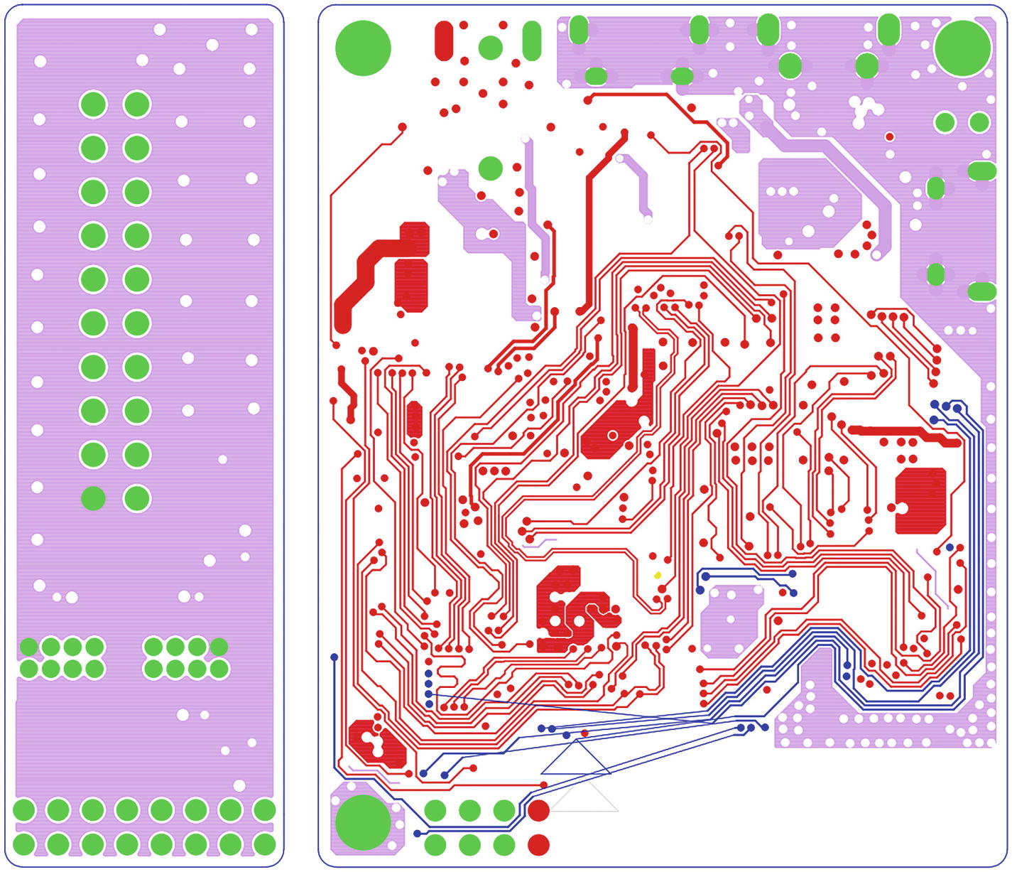
A PCB with partially completed routing
Mechanical Check
A CAD engineer can generate certain files from the electrical CAD tools for mechanical engineers. These files are required for a mechanical engineer to generate a 3D view of the PCB assembly.
This 3D view of the PCB assembly is in certain standard file format, which can be imported to any mechanical tool to check the mechanical assembly of the drone with other mechanical components already imported to the tool or designed in the same tool.
Gerber Release
Initially developed by a company with the name of Gerber, the Gerber format currently refers to a widely accepted standard capable of describing board images such as conductor layers, solder mask layers, and legend layers.
Printed circuit boards are designed in a specialized EDA (electronic design automation) or a CAD system that further generates board manufacturing data, based on which circuit board fabrications are commenced. PCB manufacturers won’t fully understand all details of a PCB design file unless a Gerber format file is generated for reference and guidelines. The Gerber format file is applied to describe the design requirement of each image of a circuit board and it can be applied for both bare board fabrication and PCB assembly.
No one needs a delayed printed circuit board project. Delayed PCBs often end in huge penalties paid to the manufacture for the wasted slots. The ideal circumstance is that you send your design file to the PCB manufacturer, and the manufacturer arranges board fabrication based on your file and delivers the products to you. The practical situation, however, is not that simple.
It usually takes a long period of time from the moment you send your design file out to the final arrival of the boards. Certain effectiveness and efficiency measures can spare you from unwanted delays in PCB manufacturing.
When it comes to bare board fabrication, the Gerber format is called for by both standard photo plotters and other manufacturing equipment desiring image data like legend printers, direct imagers, or AOI (automated/automatic optical inspection) equipment. Put simply, Gerber format files are essential from the beginning to the end of the PCB fabrication process.
When it comes to PCB assembly, a stencil layer is included in the Gerber format and component locations are regulated as well, which are regarded as significant reference data for SMT (surface mount technology) assembly, thru-hole assembly, and mix of them.
Gerber files do play a crucial role as a connector and translator between PCB design engineers and PCB manufacturers, enabling design engineers’ considerations and concepts to be understood by manufacturers so that correct and reliable products can be effectively and efficiently manufactured.
Summary
In this chapter, we discussed general and drone-specific hardware development procedures and processes. The hardware development cycle starts with the architecture block diagram, but the actual detailed design starts from the library creation and schematic design for the multiple boards in the system. Completed schematics are transferred to the layout tool with appropriate inputs and prerequisites. The prerequisites for the layout define the outline, stack-up, and the electrical and mechanical constraints. Finally, the Gerber release for all the boards required for the drone marks the end of the drone hardware design cycle, which is the half mile crossed for the entire development cycle.