This chapter will cover how you would go about designing your own circuits. It will show you where to find information about components and circuits, some tools for designing circuits, and how they can be used to create circuits, including custom printed circuit boards (PCBs). Finally, it will explain about creating a power supply suitable for powering a Raspberry Pi.
How to Design a Circuit
Designing a circuit is usually a multi-step process. First, you start with the idea, next research the available components, and then having decided on the components, design it into a circuit showing how they will be connected. You can then prototype the circuit, making a temporary circuit before creating the final finished circuit. The final circuit could be built on an off-the-shelf board such as stripboard or made into a complete printed circuit board depending upon your budget and the complexity of the circuit.
Each of these stages can be repeated as necessary until you come to the final design. As you move through the stages, the potential cost increases both in terms of money and the time taken, so the earlier you identify any potential problems, the less it will cost. Don’t be afraid to go back to the start rather than trying to continue with a design that isn’t working.
The prototyping stage is a useful stage as this is when you get to see if the circuit you have designed is likely to work. This is often done using a breadboard. You don’t necessarily need to test every single component at this level, but you should test all the basic blocks. For example, when designing the four-light disco lights, I only tested one of the MOSFET switches, and the other three followed the same design, so I did not need to test them separately. The more comprehensive your testing, the better the chance of identifying any potential problems.
There is one additional step that is used in professional circuit design, which is to perform a circuit simulation. Circuit simulation involves computer modeling of the behavior between components to see how they will work together. It can be a complicated process and should not be required for the type of circuits you will be making at this stage.
The idea is something you can come up with yourself, although hopefully some of the ideas in this book may help with getting the inspiration. This will look at some of the sources of information, and the tools you can use help design a circuit.
Datasheets
When designing circuits, you need to understand the particular characteristics of the components we use. Components that look similar to each can behave in different ways when used in practice. To get this information, manufacturers provide a datasheet which explains the characteristics of their components. Interpreting the information from a datasheet is one of the key skills when designing your own circuit.
Datasheets for different types of components may be completely different, but there are a number of sections that are often included. Rather than covering just one type, I have created a few examples of the sort of thing that you may see on a datasheet. I suggest you download some real datasheets so that you get familiar with their content. The best place to download the datasheets is normally from your component supplier. Some companies such as Farnell/Element 14 provide links to the datasheets in the component listings, some other suppliers may include practical examples and tutorials, but some suppliers do not provide any information. If you don’t find what you are looking for, then search for datasheet followed by the component name using an Internet search engine.
The first thing in a datasheet is a descriptive title, the component model number, and the name of the manufacturer. This is normally followed by a paragraph explaining what the component is and where it is useful. In some cases, a single datasheet may include multiple components (such as the TSOP2438 infrared receiver which shares a single datasheet with 23 other similar receivers).
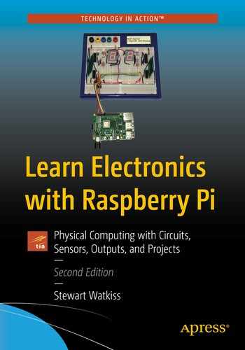
Pin layout for the MCP3004
This is the MCP3004 analog-to-digital integrated circuit that we used in Chapter 6. This has been chosen as it is a good example of the different types of pin labels that you may come across.
The numbers on the inside of the IC are the pin numbers. Pin 1 is indicated at the top left which is normally physically identified on the chip by a semicircle or small dot on the side with pin 1. CH0–CH3 are the input channels (analog inputs). NC means not connected; this normally means that it is not used and so the pin should be left without physically connecting to the rest of the circuit. Normally, GND is used to signify the pin that needs to be connected to the 0V ground part of the circuit. In this case, it has a separate ground connection for the digital and analog parts of the circuit indicated by DGND and AGND, respectively. An alternative is VSS which is used by some manufacturers to refer to ground instead.
The pin marked CS/SHDN is used for chip select or to shut down the input. An alternative that you may see for some components is EN which stands for enable and normally means the same as chip select. You will see that there is a line above CS. This indicates that it is inverted, so a high input has the opposite meaning as the wording. In this case, “chip select” happens when it receives a low signal rather than a high signal.
The pins labeled as DIN and DOUT are the data in and out pins used to communicate with the Raspberry Pi using I2C. CLK stands for clock where a timing signal is required. The VREF pin is used for the analog part of the circuit as a reference voltage that the input is compared against. Finally, the VDD pin is connected to the positive power supply; on some circuits, this may be VCC instead.
The pin layout may also show different variants of the component. This may include an option for a surface mount device (SMD) or through the hole device. You will normally want to avoid the SMD components when first creating your own circuits as they can be difficult to solder.
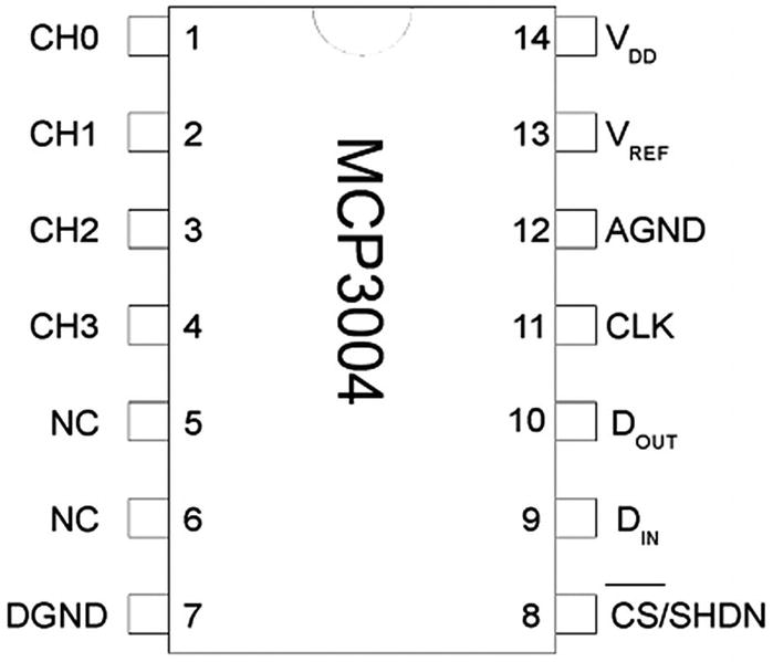
The next part of the datasheet is often a table of absolute maximum ratings, which are values that should not be exceeded. Going outside of these ranges will mean that the component may not operate correctly or may cause permanent damage to the component.
Absolute maximum ratings for the IRL520 MOSFET
This shows the maximum voltages between different pairs of pins as well as the continuous and pulsed currents. Exceeding these values is likely to damage the MOSFET. Also note that some values may depend upon certain conditions, and in this case, the maximum drain current is less as the temperature increases.
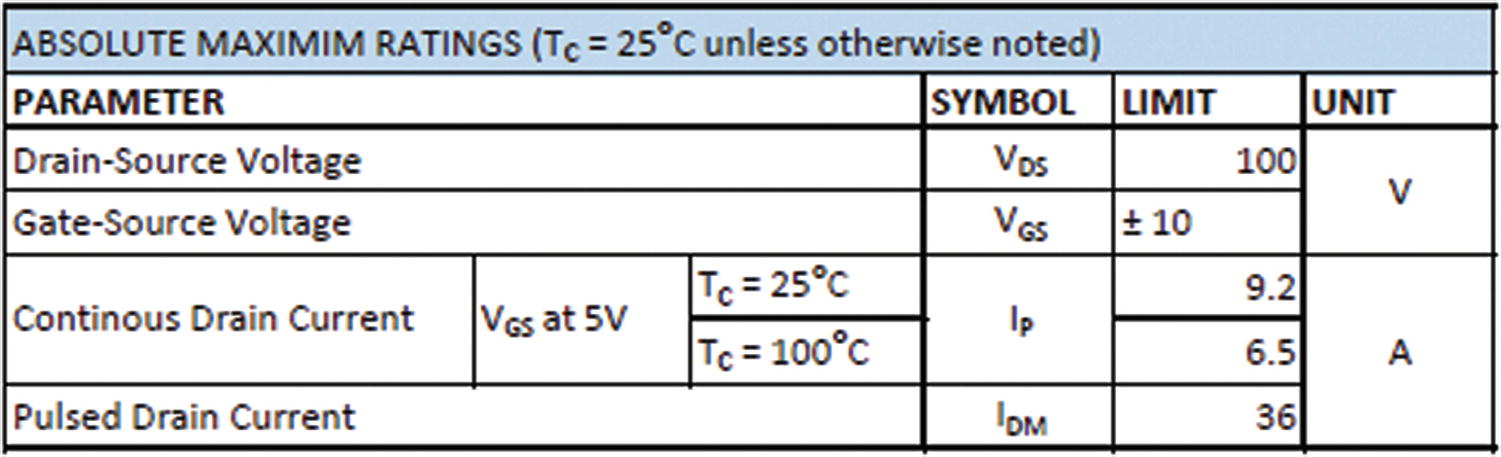
There are then often several tables providing more information about the behavior of the component under certain conditions. For logic circuits, this will include the valid voltage ranges for a signal to be considered as a true or false; for a transistor, it will include the typical gain; and for an LED, it may include the luminous intensity. There may be other information that is useful under certain circumstances such as timing information or effective capacitance.
Sometimes it is not possible to put the information into a table as the information may vary depending upon the input, temperature, or other characteristic. In this case, the information may be presented as graphs or timing diagrams.

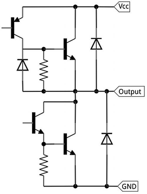
Open collector used on certain ICs
Datasheet representation of output from SN754410 H-bridge IC
The datasheet may also include examples of how the component can be used in a circuit and often includes the dimensions of the component and how it connects to a printed circuit board.
Some datasheets will be more useful than others, but as you can see, it can be an invaluable source of information when designing a circuit.
Introduction to Fritzing
If you want to run Fritzing on something other than a Raspberry Pi, then you can pay to download the software, which will allow you to download the latest version and to help support future development of the software.
Designing a Circuit Diagram/Schematic
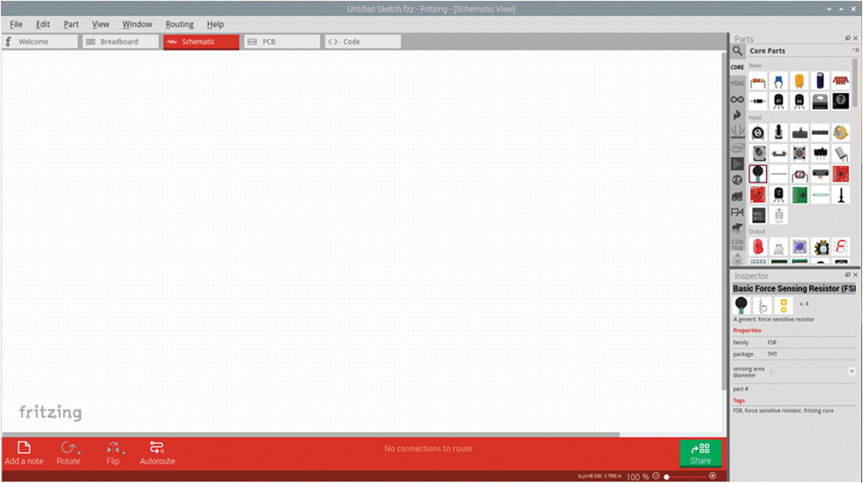
Fritzing schematic view
The main part of the screen contains an editor area, which is a white background with a grid for laying out the circuit design. The area to the top right is labeled parts which contains the available components and circuit boards, and the inspector area at the bottom right will allow you to change any of the parameters relating to the current component.
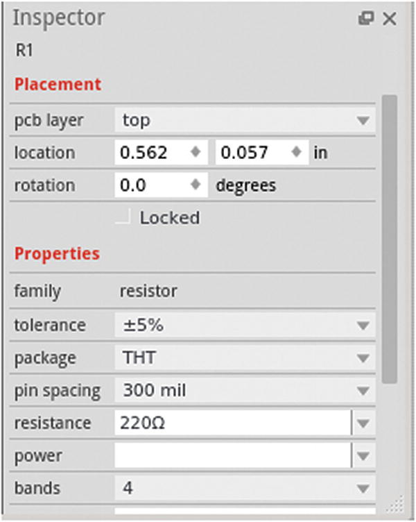
Fritzing inspector panel for a resistor
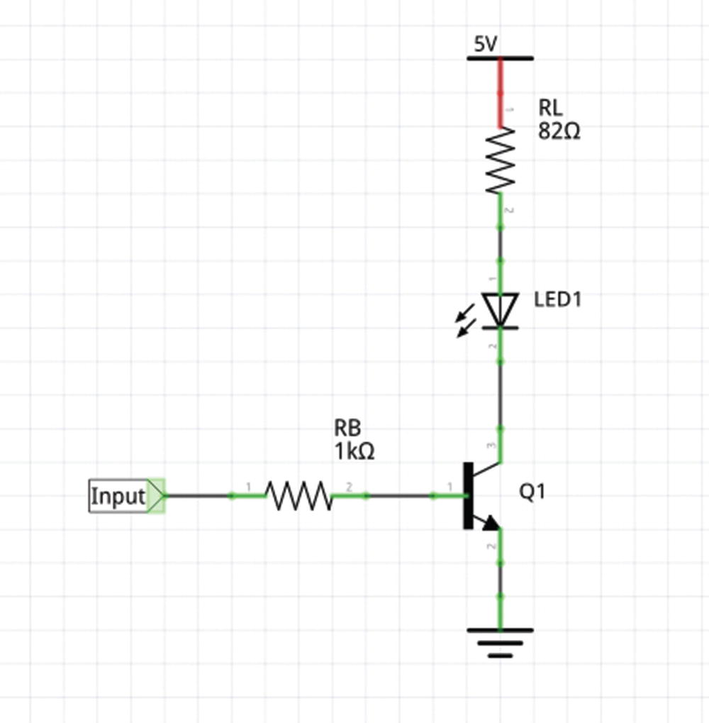
Transistor LED circuit schematic view
I haven’t included the Raspberry Pi on this diagram, although you can include one by dragging it from the core components. In this case, I have used a net label at the point where the circuit connects to the GPIO, instead of showing the Raspberry Pi on the diagram.
Rules when Designing a Circuit
The positive supply is usually placed at the top of the diagram.
The ground (0V) supply is normally placed at the bottom of the diagram.
- Inputs are normally positioned toward the left and outputs toward the right.
As a result, the data signals normally flow from left to right.
If a battery is being used, then this may be displayed using the battery symbol, but often the supply is shown by marking the appropriate lines instead.
Lines are normally drawn horizontally or vertically straight. A change in direction is normally through a 90-degree turn. In Fritzing, the connections will normally take the shortest path, but can be dragged out to form 90-degree turns.
- Avoid crossing lines where possible.
Where lines join, a dot (filled circle) is used to indicate a join.
Where lines cross but don’t join, they normally pass in a straight line.
- Each component is normally given a reference. This is prefixed with a letter or few letters to denote the type of component. Examples include
R for resistor
D for diode
Q for transistor
BT for battery
C for capacitor
Creating a Breadboard Layout
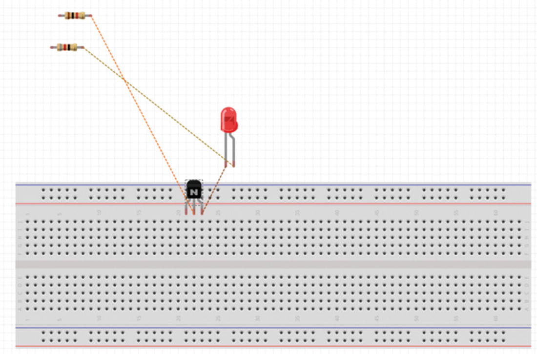
Fritzing initial breadboard view
Not only does this look a mess, but for some circuits, components will be on top of each other hiding those below them. First, you should click the breadboard and use the inspector to set it to the appropriate type of breadboard. The most common breadboard is the half+ breadboard.

Fritzing updated breadboard view
The resistor going to the base of the transistor would normally connect to the Raspberry Pi, but I have not shown the Raspberry Pi in this view.
Creating a Stripboard Layout
If you would like to create a layout for a stripboard, then that is done using the same breadboard view. You will lose the view of the breadboard, so you may want to save that with a different name first. Click the breadboard and choose delete and then drag the stripboard part from the core parts. There are only a couple of different types of stripboard included, but you can adjust the number of columns and rows. You can also create breaks in the rows by clicking the stripboard between a pair of holes.
Designing a PCB
Fritzing can also be used for creating a professional printed circuit board (PCB). In the past, it was expensive to get custom PCBs made, but it has come down considerably in price and can provide a professional look for your project. The price for PCBs varies depending upon manufacturer, lead time, and quantity. The quantity is an important factor as buying in bulk can be much cheaper, but you will want to test your PCB design first.
This is a very simple circuit, so it doesn’t really need its own PCB, but it is useful for illustrating the process of designing a PCB. Clicking the PCB tab shows a gray area for the PCB board. You will find all your components stacked up on the top corner which will need to be moved around.
First, set the size of the PCB and move the components to appropriate positions on the board. Before you go about working out how the copper will be laid out, you need to add some way of connecting to the power supply and to the Raspberry Pi. For the power supply, you can use one of the included power connectors, and for the Raspberry Pi, you may want to include a 30-way connector, but both these would be overkill for such a simple design, so I instead used three terminals, two for the power supply and one for the GPIO connection. I used the part for a terminal connector, but you could just solder wires directly to the pins rather than using a physical connector.

Initial PCB layout without routing
The next stage is to add the copper tracks which go between each component. There is an Autoroute option, but you can do this manually similar to the breadboard layout using the dotted lines as a guide. There will be no connections shown to the connector terminal, so you will need to add these as well. Before you start dragging out the connections, you may want to specify which layer to run the connections on. While technically it doesn’t really matter whether these are on the top or the bottom, I normally prefer to put as many on the bottom as possible; this is more from my experience creating single layer boards in the past. To do this, look for the icon on the bottom that says “Both Layers” and choose “set bottom layer clickable”. Any tracks you draw will be orange, indicating that they are on the bottom; if you change it to the top layer, then they will be colored yellow.
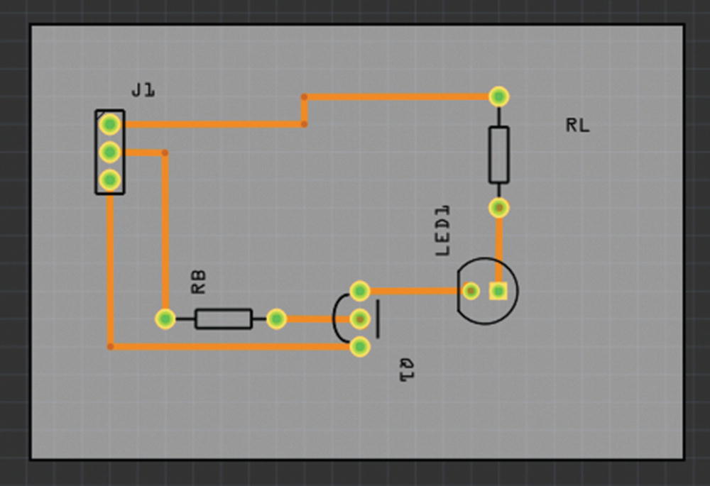
PCB layout with copper tracks between the components
If you now switch to the schematic view, you will see that the connector component has been added and that it has dashed connections to the power supply and resistor RB. This is one of the features of Fritzing as you can add a component in any of the different views, and it is added to all the others. You may want to tidy the other diagrams up by repositioning the connector and wires. Alternatively, if you didn’t want to show the wires, you can use the “Delete ratsnest line” to hide the dashed line. Take care when using this option as it is a useful way to check that you have connected up your circuits correctly.
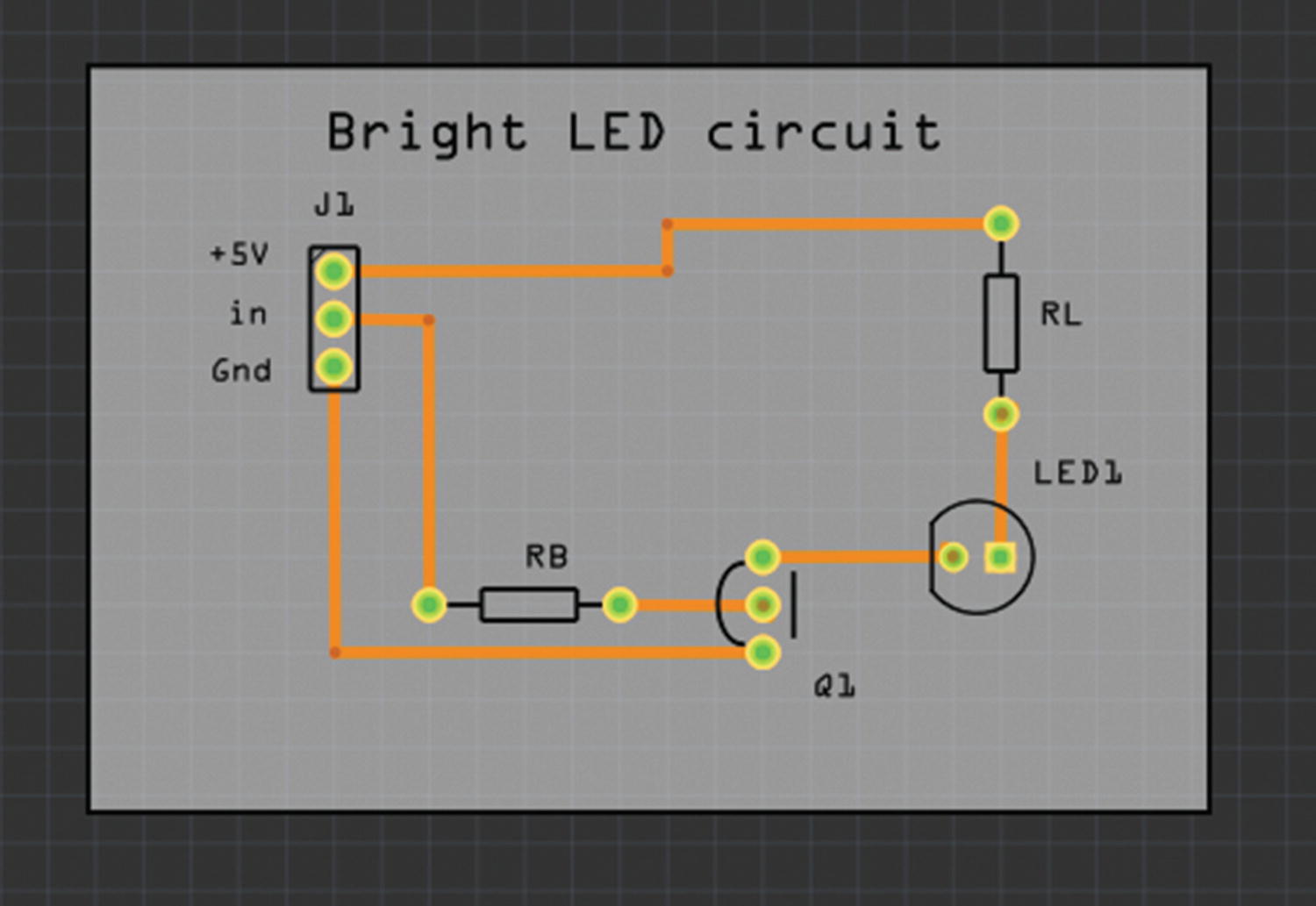
PCB layout with added text information
This is almost ready to have made up as a printed circuit board. The final thing you should do to the design is to add a ground or copper fill. This will fill most of the PCB with copper, and in the case of a ground fill, it will be connected to ground which can help with avoiding electromagnetic interference. To add a ground fill, right-click the Gnd connection and choose Set Ground Fill Seed, and then from the Routing menu, choose to apply a ground fill. The entire board will then be filled in with copper, except for a gap around each of the connections. If you look at the bottom layer, you should see that the ground connection from the connector to Q1 is merged into the ground fill.
The PCB is now ready to be sent for manufacturing. Before actually sending it off, it is a good idea to perform some checks on the finished layout. First, run the Design Rules Check (DRC) from the routing menu, which will check for any common problems. Then export the PCB layout using the File ➤ Export for Production and choosing PDF. Print off the component layout and check that the components fit. Double-check that all the components oriented correctly on the PCB layout.
Once you’ve checked everything twice, check it once more before you send the files to the manufacturer. Remember the extra cost and time if there is a mistake. If you want to use the Fritzing lab (which funds the development of Fritzing software), then you can use the Fabricate button which will load a web page for submission. There are a couple of advantages to using Fritzing. The first is that you can just send the Fritzing file as it is, and the second is that they will perform some additional checks. It can be more expensive than some other manufacturers.
If you would rather send to a different PCB manufacturer, then you can export for production as extended Gerber files. You may need to fine-tune some of these files and check the submission rules, especially what files they expect to receive.
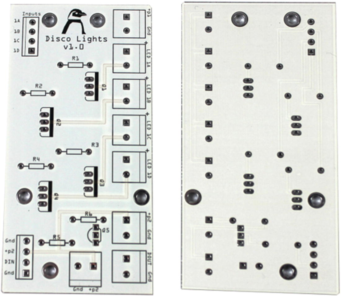
Manufactured PCB for disco lights and NeoPixels
Powering the Raspberry Pi
The Raspberry Pi is normally powered from a dedicated power supply through either a USB-C or micro-USB connector. This is fine for normal use, but what if you want to include the Raspberry Pi into a complete project that already has a power supply? When I created the disco light project which runs on 12V, I didn’t want to have to add a second power supply for the 5V needed by the Raspberry Pi. You can make a power supply yourself; this is useful to understand how you can add a power supply directly into your own circuit. You can however buy more efficient solution that can be easily connected into the circuit.
78xx Linear Voltage Regulator
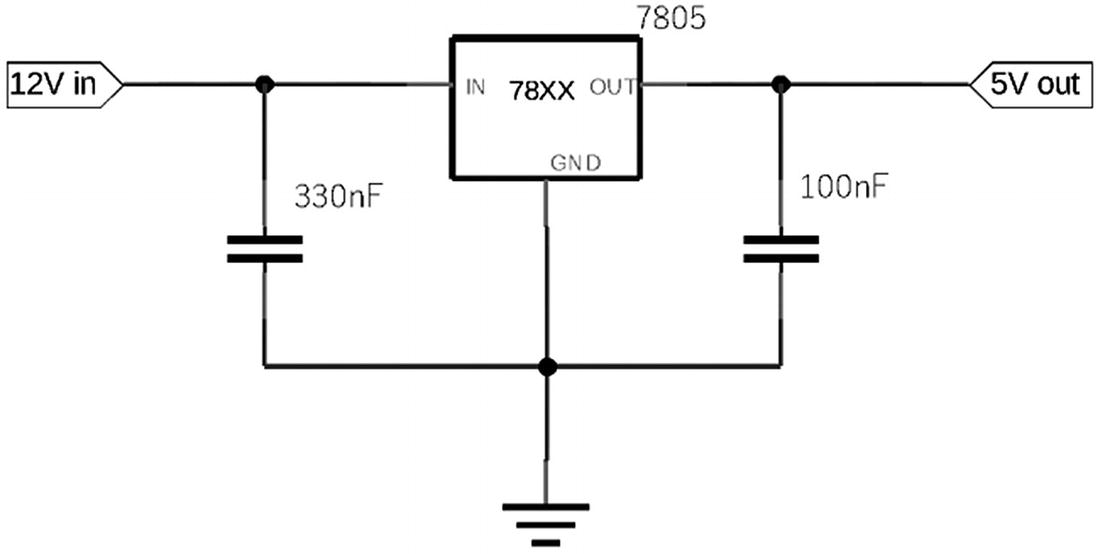
7805 voltage regulator circuit
The voltage regulator comes with a variety of different output voltages, which are denoted by the last two digits. For example, the 5V regulator suitable for the Raspberry Pi is the 7805. The input voltage needs to be higher than the output voltage and in the case of the 7805 needs to be at least 7.3V.
One disadvantage of a linear regulator is that the voltage difference between the input and output is turned into heat which wastes power. If this is supplying 600mA (a typical current draw for a Raspberry Pi 3) using a 12V power supply, then the amount of power lost would be 4.2 watts (7V dropped x 0.6A). This is quite a significant amount of heat, and a heat sink would be required to prevent the regulator overheating.
Buck Converter
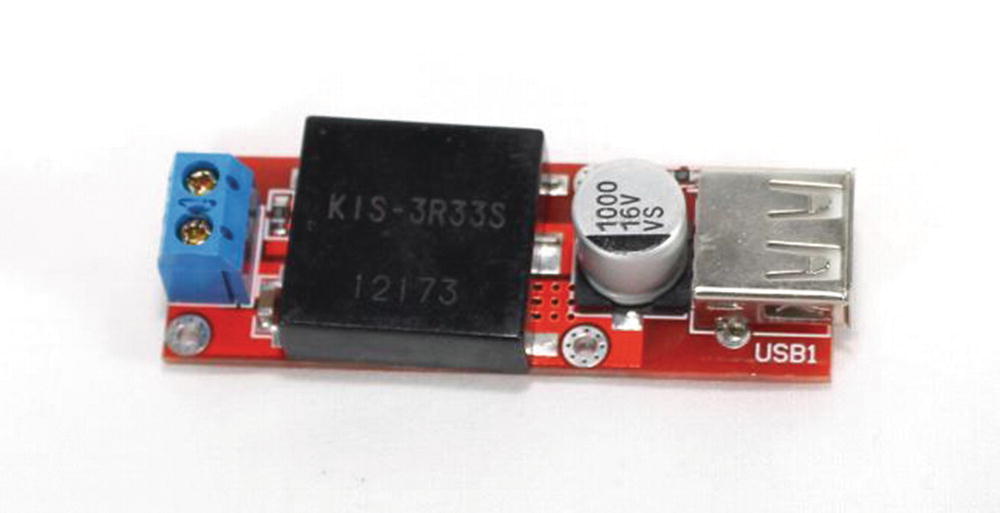
Buck converter
A buck converter is available through various suppliers such as Amazon Marketplace or eBay. These are more expensive than the linear voltage regulator, and they take up more space but are better where power efficiency is concerned.
Always check the output from a buck converter before connecting it to your Raspberry Pi. I learned this from experience when the one I purchased gave too high a voltage, damaging the Raspberry Pi.
Designing More Circuits
In this chapter, you have looked at the information needed to design your own circuits. This has shown how datasheets provide the information needed when designing a circuit and how to extract the relevant information. It then looked at Fritzing and how it can be used to design circuits, including creating a schematic layout, designing a breadboard and stripboard layout, and finally creating a professional printed circuit board.
This chapter provides the basics for getting started with Fritzing, but only scratches the surface of what Fritzing can do. I encourage you to spend more time learning about Fritzing. There are also other circuit design software such as KiCad (which is open source software) and EAGLE PCB design software which is a commercial product but free to use for small circuits. Neither of these provides the ease of use and breadboard layouts that Fritzing does.
Through this book, you have learned about electronic circuits, about how to connect them to the Raspberry Pi, and the steps involved in designing your own circuit. With this information, you can now design your own electronic circuits to have the Raspberry Pi interact with the real world.
Look around at what others have made, come up with your own ideas, and design your own electronic circuits.