
Digital logic is the basis around how all digital electronics work including the basic building blocks for creating a computer such as a Raspberry Pi. It’s an interesting subject, but there is too much to cover just using practical projects. This chapter is therefore going to be more about the theory rather than learning through practical projects. At the end of the chapter, there will still be a practical element, which is based around 7-segment LED displays.
Some of the concepts on here are better explained through animation. I have created some videos which explain some of these concepts, which are on my website at www.penguintutor.com/electronics/digital.
Digital Logic and Binary
When talking about digital electronics, such as microprocessors and computers, information is represented by switches that turn the voltage between high and low. This has already been covered when using the GPIO ports where the output has been turned on or off which represent the high and low states. On the Raspberry Pi, there is no way of turning a GPIO port partway on; PWM was used to create the illusion of the port being partly turned on, but that was actually achieved by turning the output high and low quickly.
With only a single output, it is only possible to hold a tiny amount of data, but when multiple outputs are used together or a switch is turned on and off in a specific sequence, this can be used to represent anything you want. To provide meaningful data, the information is stored and manipulated using the binary numeral system.
Binary is a base-two number system with each digit either a 0 (which is represented in electronics as a logic low, such as 0V) or a 1 (which is represented in electronics as a logic high, such as 3.3V). Within processors, the information is grouped into multiple bits; it was common to have 8 bits which makes a byte, although most computers now are either 32-bit or 64-bit. Using a single byte which is 8 bits long, it is possible to represent up to 256 different values, which go from 000000002 (decimal 0) to 111111112 (decimal 255). Showing each entry as individual bits takes up a lot of characters, so it is common to show these as hexadecimal values, where 4 bits is replaced by a single hexadecimal character from 0 to F (where letters are used for values above 9). The maximum 8-bit number of is 111111112, represented as FF16. You may have already used hexadecimal values when dealing with colors in HTML.
The information in the binary numbers can be in parallel, which is across multiple wires known as a bus, or transmitted as a serial signal over a single wire. A bus is used internally within a processor and for connecting to memory, whereas serial transmission is normally used for connecting to external devices such as over USB .
Logic Gates
The basic building blocks used to create digital circuits are logic gates. There are four primary logic gates – NOT, AND, OR, and XOR, which can then be combined to create more complicated circuits. These are represented by circuit symbols used in schematic diagrams, as with other symbols, there are different standards. There are two shown for each, one of which is based around a distinctive shape for each gate and the other is based on a rectangular block. The logic gates are available packaged in integrated circuit (typically, 4 to 8 in a single IC) or are incorporated into more complicated circuits, which use the logic gates as building blocks.
NOT Gate (Inverter)
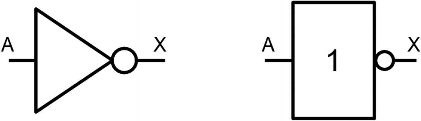
Circuit symbols for a logic NOT gate
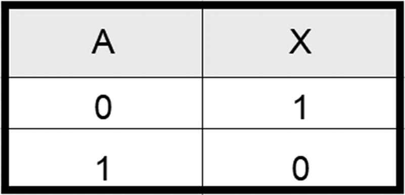
Truth table for a NOT gate
The truth table shows all possible inputs (A) and the corresponding outputs (X). The inputs are denoted by letters from the start of the alphabet, whereas the outputs are denoted by letters near the end of the alphabet; this is a convention that makes it easy to understand the difference between inputs and outputs.

Example circuit for a MOSFET NOT gate
When the input is low, the MOSFET is switched off. The output is pulled high through resistor RL. When the input is high, the transistor switches on pulling the output low.
The circuit shown is just an illustration of how a NOT gate can be created. The circuit within a logic gate IC is more complicated than this. The output stage normally includes a p-type MOSFET in place of the resistor RL. The p-type MOSFET would operate the opposite to the n-type MOSFET. This means that the output is actively pulled up and pulled down instead of using a passive pull-up resistor. This allows the output to drive a bigger load and maintains the logic levels better. Using a n-type and p-type MOSFET in this way is known as CMOS (complementary metal-oxide-semiconductor). The input stage may also include additional components such as additional diodes to protect against a higher input voltage or static electricity.
AND Gate
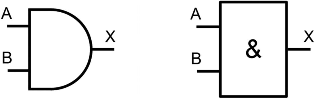
Circuit symbols for a logic AND gate

Truth table for an AND gate
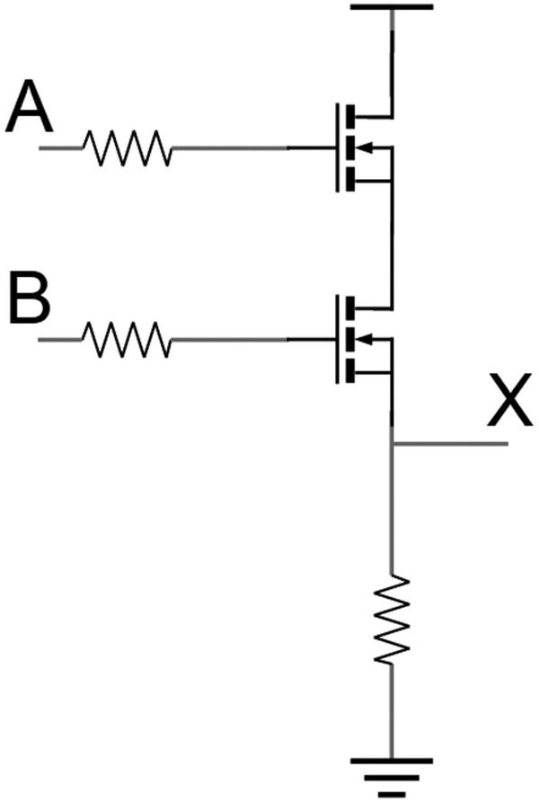
Circuit demonstrating how an AND gate works
OR Gate

Circuit symbols for a logic AND gate

Truth table for an OR gate

Circuit demonstrating how an OR gate works
As you can see from this diagram, there are two paths between the positive supply and the output. If either of the MOSFETs is turned on, then the output is high.
XOR Gate

Circuit symbols for a logic AND gate
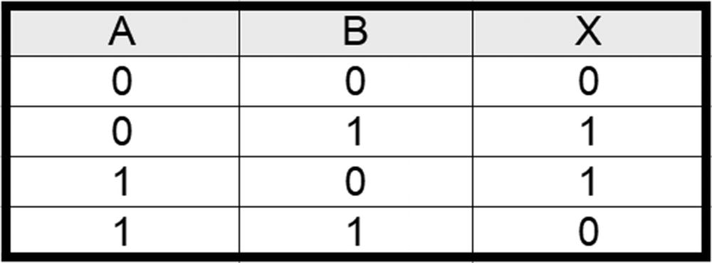
Truth table for an XOR gate
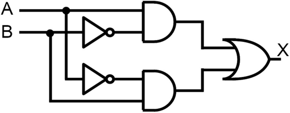
Logic circuit for an XOR gate using NOT, AND, and OR gates
This logic circuit diagram is significant as it shows how more complex operations can be made by joining logic gates together. In this case, the top AND gate has a high output if A is high and B is low. The bottom AND gate has a high output if A is low and B is high. Then the OR gate gives a high output if either of the two AND gates is high. This way, the output X is high when one input is high and the other is low.
NAND and NOR
Previously, I listed the four primary logic gates as NOT, AND, OR, and XOR; however, perhaps more important are the NAND and NOR gates. The NAND gate is effectively an AND gate, followed by a NOT gate, and the NOR gate is an OR gate, followed by a NOT gate. These are known as the complements of the AND and OR gates. These were made popular because they could be created more simply, but also could mimic the other logic gates. In that way, it is possible to take a circuit that uses any of the four logic gates and replace it with a circuit that uses just NAND or NOT gates. This was significant when circuits were created using logic ICs.

Circuit symbols for logic NAND and NOR gates
Creating Logic Circuits – Adder
Using the different logic gates, it is possible to combine them into a more complicated circuit. An important function in microprocessors is the ability to add numbers together. Addition forms the basis of many mathematical operations in a computer and is also needed for counters which keep track of whereabouts the next instruction is in the program code.
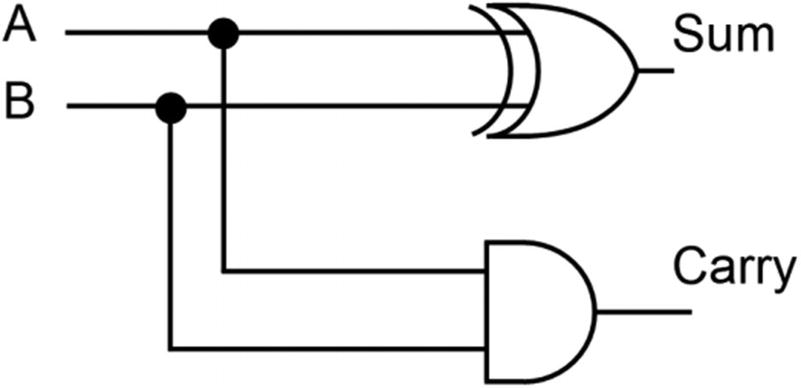
Half adder circuit
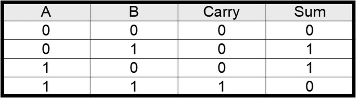
Truth table for a half adder
The reason that this is known as a half adder is because while there is a carry out, there is no carry in. If we want to use this on a more inputs (such as an 8-bit number), then there needs to be some way of including the carry in from the lower bit.

Full adder circuit
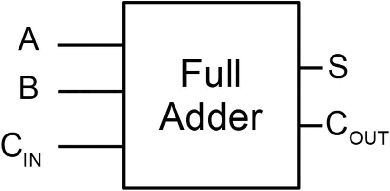
Circuit symbol for a full adder
As you can see, the complexity of the previous circuit is hidden in a single rectangle, which is labeled with the function of the circuit. This is commonly used for many different circuits to make it easier to understand and reduce the size of the diagrams.
In the case of an 8-bit adder, the symbol could be replaced with a single block with the single input A replaced with inputs A0–A7 and the same for the B inputs and the sum outputs. There will only be one carry in and carry out as the others are used internally.
This technique for simplifying circuit diagrams can be used for any level of complexity even to the point where it is used to represent the entire computer. This has already been used in numerous diagrams in this book where the Raspberry Pi is shown as a single block.
Using multiple full adders to create an adder does have a disadvantage when it comes to speed. Logic circuits act very quickly, but when chained together, the small delays can add up. In the case of the adder, the least significant bit performs the add before passing the carry out to the next stage. The output of the next stage in the adder is dependent upon that carry out from the first stage. This is known as a ripple carry adder. It is possible to instead have a fast adder which can calculate each bit of the number simultaneously, although the circuitry is increasingly complex.
Flip-Flops
The adder circuit is an example of a combinational logic circuit. This means that (except for the delay in updating the outputs) the logic output is entirely dependent upon the inputs at the time. It is sometimes necessary to store information either as a form of short-term memory (such as a register in a processor) or so that the information is presented to other stages of the circuit when they are ready to receive it. This needs sequential logic, of which the most basic form is the flip-flop. There are several different types of flip-flops, three of which are explained as follows.
Basic Flip-Flop

Basic flip-flop with NOR gates
The flip-flop has two inputs, called set and reset. There are two outputs Q and Q'; these are complementary outputs. The Q is the data output and Q' the complement (opposite) of that output. The set input is used to set the flip-flop to the set state (Q=1), and the reset puts the flip-flop into the reset state (Q=0). I have labeled the NOR gates as A and B; this is purely to make the explanation easier.
The output from each of the NOR gates is used as an input to the opposite gate. This is feedback used to maintain the state of the flip-flop.
The initial state cannot be determined until either set or reset is taken high. When set is taken high (S=1), at least one input of B is 1 and then the output of the B=0. Assuming R=0, the output of the A depends upon the output of B. With B=0, A=1 and so the output Q=1. If set goes to 0, then gate B still has a high input from the output of A and so B=0. As such, the flip-flop maintains the set state and Q=1.
If set is at 0 and reset is set to 1, then A=0, which sets the output Q=0. As both inputs to B are now 0, B=1. If the reset now goes to 0, then the reset state is maintained by the feedback.
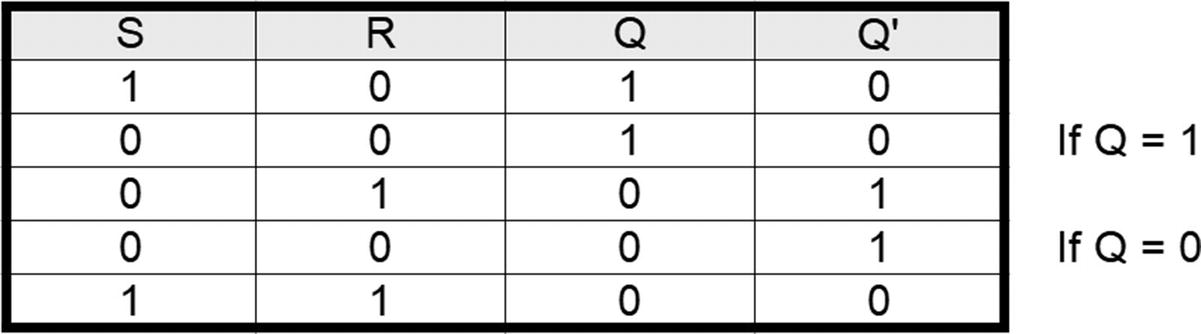
Truth table for a basic NOR flip-flop
This truth table is different from the previous ones, in that there are now two lines with the same inputs (S=0 and R=0) but different outputs. This is because they are dependent upon the previous state. The final entry, where set and reset are both high, is invalid as both Q and its complement are the same. This state should be avoided when using flip-flops.
This basic flip-flop is useful for understanding how a flip-flop works, although the flip-flops that are normally used also include a clock signal.
SR Flip-Flop
The basic flip-flop provides the set and reset function that the SR flip-flop uses. The flip-flops that are used in most circuits had the added ability to determine at what point in time the data is stored into the flip-flop. This is done by adding either an enable signal (which is triggered by logical level) or a clock signal (which is edge triggered), so that the state of the flip-flop only changes when ready.
This is important when the flip-flop takes an input from a previous stage where there may be a delay before the data is valid. For example, with the ripple adder, there is a state where the output may change based on its inputs, but because the carry has not yet rippled through, the output is incorrect. In this case, the enable or clock signal would only be triggered after there has been time for the adder to complete its calculation.

SR flip-flops with different enable and clock types
The symbol on the left is based on an enable input. The state of the flip-flop can change only when the enable (E) is high. If that signal is set permanently high, then it will operate the same as the basic flip-flop.
You will also note that the complementary output Q' is shown as Q with a line over it. These mean the same thing, that the output is the opposite of Q. The line above the output is often used in diagrams but is difficult to include in printed text so is sometimes replaced with Q'. It is also common to see inputs with a line over them, particularly the enable pin; this indicates that the input is based on the enable being low instead of high.
The other symbols show an arrow to indicate it is an edge-triggered clock signal. The default is for a positive edge trigger (when the clock changes from low to high), and the circle denotes a negative edge trigger (when the clock changes from high to low).
You may also see reference to an RS flip-flop. The RS flip-flop is the same as the SR flip-flop in normal operations. They behave differently in the condition where set and reset are high. If this condition is triggered, then with the SR flip-flop the set takes precedent and with the RS flip-flop the reset takes precedent.
D Flip-Flop
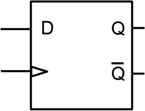
Symbol for a D flip-flop
One side effect of the D flip-flop is that it no longer has the invalid state, where both set and reset are triggered together. It does still have the state at the beginning when the status is undetermined.
Other Flip-Flops
There are other flip-flops and variations on the ones already shown. Some flip-flops have both enable and clock inputs allowing the clock to be connected to the system clock but only updating when enabled. Some also have additional inputs to set the flip-flop to a pre-determined state to avoid the unknown state when first turned on.
Connecting eight flip-flops side by side but sharing a single clock is known as an 8-bit latch, also known as an 8-bit register. Registers are a fundamental part of how computers work, allowing data to be held temporarily when retrieving from memory or for use as the input or output of any calculations within the processor.
Shift Register
Another use of flip-flops is to create a shift register, which is useful for converting serial data to parallel data. This will be used in an example circuit to reduce the number of pins needed to connect 7-segment LED displays to the Raspberry Pi GPIO.
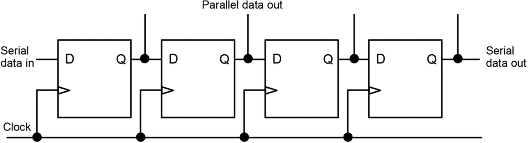
Shift register circuit
The example shows four stages in the shift register, although I will describe this in terms of an 8-bit shift register, which will be used for the practical example. As you can see, each of the flip-flops is connected using the output from the previous (Q) as the input to the next stage (D). They all share a common clock, so data is transferred simultaneously at each stage. The serial data goes into the first D flip-flop and is saved on the first clock pulse. The serial input is then set to the next bit of information, and on the next clock pulse, the data that is on the first flip-flop is passed to the next one and the new data is stored on the first flip-flop. This continues until all the data is shifted in; for an 8-bit shift register, this takes eight clock pulses. At that point, parallel out is now a parallel version of the serial data. There is also a serial data out which can be used for connecting to another shift register. This allows multiple shift registers to be connected without needing any additional outputs from the Raspberry Pi (or other driving circuit), but that is at the cost of time as that means that more data needs to be shifted through the shift registers.
In most circumstances, you would not want to see the data going through the shift register, so the parallel output should not change until all 8 bits have been sent through the register. To do this, we need an output register, or a latch, which is another use of the D flip-flop. In effect for each bit of data, there will be one D flip-flop for shifting the data in and one D flip-flop for latching that data to the output. A second clock is needed for the output, but that only triggers once for every eight pulses of the serial clock.
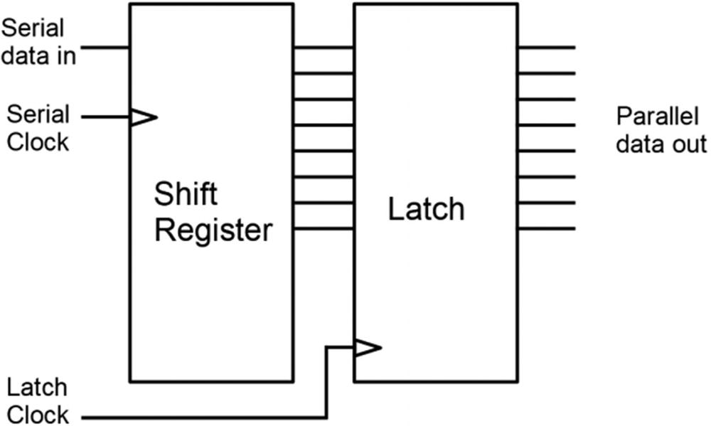
Shift to parallel shift register with latch
This diagram shows the shift register used to convert the serial data into parallel data, which is then fed into the latch. The shift register and latch have their own clock signal so that the latch only updates the parallel data out when the latch clock is triggered.
If you are looking to buy a shift register as an integrated circuit, then you do not need to buy the latch separately as the IC will include both. It may also have additional circuitry for output enable and sometimes an additional output buffer stage for driving large currents. One such example is the TPIC6B595 8-bit shift register, which is used in the next circuit.
Shift Register LED Circuit
After covering the theory of digital logic, it is now possible to put that into practice in a useful circuit. This will be a shift register that will provide eight outputs from the Raspberry Pi using only three pins from the GPIO. This will be used to drive LEDs.
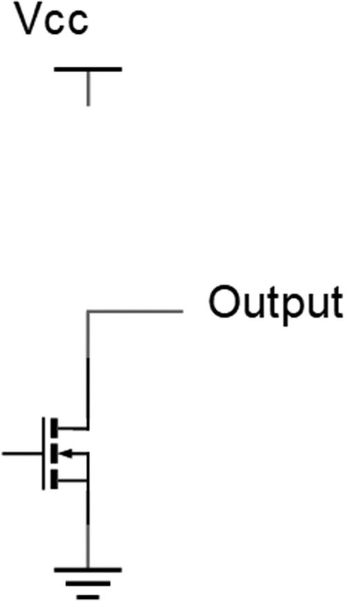
Open-drain output
Another benefit to having an open-drain output is that a different supply voltage can be used for the load. This is useful if switching loads that need a different voltage.
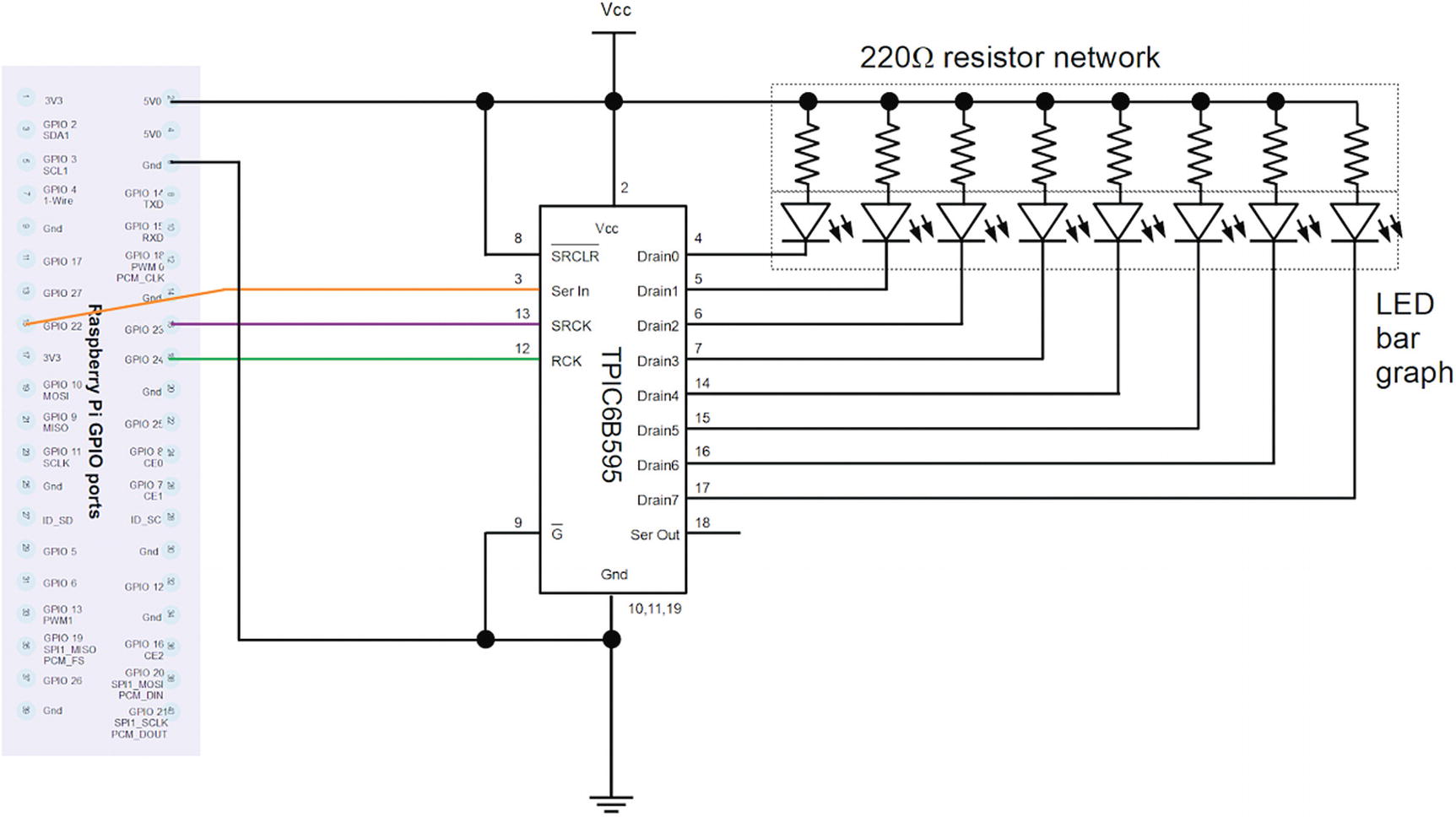
Shift register LED display circuit
For this circuit, I have used a resistor network, which is eight resistors in a single package with a common connection. I have also used an LED bar graph display. The LED has ten LEDs in a single module, although I am only using eight of the LEDs for this circuit. The LED display and resistor network are for convenience, and to make it easier to see the individual lights, these can be substituted for standard 220Ω resistors and normal LEDs instead.
Shift register demonstration program
The code has four functions. The first is shift_bit, which shifts a single bit of data into the serial port. It does this by setting the serial output to the value and then sending a 1ms pulse on the serial clock signal. The next function is register_update, which sends a 1ms pulse on the register clock signal to send the value in the shift register to the output register. Using these two functions, you can manually send a bit at a time to the shift register. The next two are used to send a word at a time. The function shift_byte is the normal operation of a shift register sending 8 bits of serial data. It uses a bitwise AND (&) to extract the least significant bit and send that to the shift register. It then uses the bitwise right shift (>>=1) to shift the variable along one bit. Once all 8 bits have been sent, it calls register_update. The final function slow_shift_byte is similar to the shift_byte, but it runs register_update after each bit and has a delay, so you can see as each bit is shifted through the shift register.
The rest of the code provides a short demonstration – first resetting the shift register to all zeros and then running two slow shift examples so you can see the individual bits being pushed through the shift register. It then has two examples using normal operation where the output of the shift register does not change until all 8 bits have been sent.
This will count from 0 to 255, which is the full range of values that can be stored in an 8-bit number.
Logic Levels
If you build the circuit in Figure 11-25, then it will almost certainly work. However, note that I said “almost certainly”; it is technically an invalid design, so there is a chance it will not (although I expect only a slim chance it will not work). The reason that the design is invalid is because the Raspberry Pi GPIO and the TPIC6B595 are designed for different logic voltage levels. The Raspberry Pi GPIO is designed for 3.3V, whereas the TPIC6B595 for 5V. There is no danger of damage to the components, as the output is lower than the expected voltage, which may not be the case if it was the other way around. If you put the output from a 5V circuit into a 3.3V Raspberry Pi pin configured for input, then there is a high possibility you will damage the Raspberry Pi.
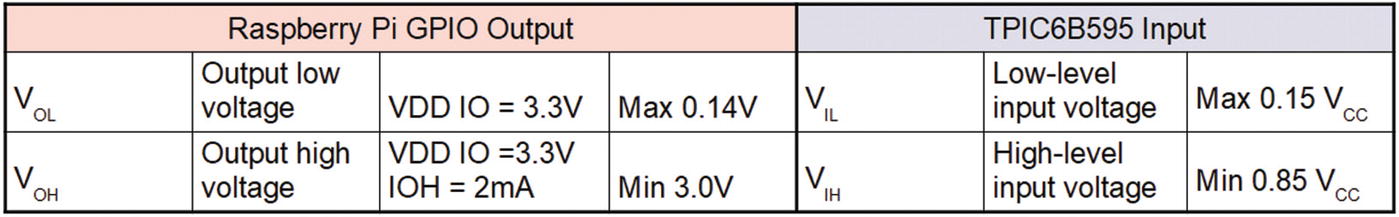
Table showing specified logic voltage levels
The values on the left show the logic level output from the Raspberry Pi. In the case of a logic low, the value will be no more than 0.14V and in a logic high (assuming 2mA output) will be at least 3.0V. The inputs to the TPIC6B595 are provided in terms of the supply voltage VCC. This says the input for a logic low should be no more than 0.15 x VCC and the input for a logic high should be at least 0.85 x VCC. With the supply voltage as 5V, this means that a low input must be no more than 0.75V (so the Raspberry Pi low signal is compatible) and a high voltage of at least 4.25V (of which the Raspberry Pi GPIO value is too low).
Looking at the input to the TPIC6B595, there is a range of voltages from 0.75V to 4.25V where the input voltage is out of the specified range. What happens if the voltage is in that unspecified area? In actual use, you will find that the shift register accepts a voltage much lower than the 4.25V as a high signal, but that is not guaranteed. Likewise, the Raspberry Pi GPIO high output is most likely higher than the 3.0V, nearer to 3.3V, but again that is not guaranteed.
There are different approaches that can be taken regarding this potential problem.
First, the option I have taken here is test it and see if it works. In this case, despite being out of the design specification, it does work, and it provides what I needed for this demonstration. There are several problems with this approach. Different ICs may have a different tolerance, and under different conditions, the voltage from the GPIO may be different, so it is possible for it to work on one setup, but not on another. It can also be very difficult to debug if it doesn’t work. This option of leaving the circuit as it is does however have the advantage of simplicity and so is something you may want to consider, especially if it’s just a personal project or a prototype to be developed further.
Another approach may be to reduce the voltage of the supply. As the minimum logic level is related to the supply voltage, it may be possible to reduce the supply voltage of the shift register. In the case of this IC, it can run as low as 4.5V, which gives a minimum input voltage of 3.8V. It is still not within the guaranteed output of the GPIO, but it has brought it closer and so more likely to work reliably.
If you still want to use this IC and want to ensure if it meets the design tolerances, then the last option is to increase the voltage from the GPIO using a buffer or level shifter. This has already been explained in Chapter 6, and a suitable circuit has been included in Figure 6-2. There are only three connections from the Raspberry Pi to the shift register, so that will need three MOSFETs and associated resistors.
The alternative is to look at an alternative IC, combination of ICs, or other circuit. I looked around and could not find a suitable shift register with open-drain outputs that is compatible with the 3.3V GPIO of the Raspberry Pi. I did however find a shift register with latch that is compatible with the 3.3V supply of the Raspberry Pi, which is the SN74HC595. The SN74HC595 can be run with a supply voltage of between 2 and 6 volts. Using it at 3.3V is fully compatible with the voltage level from the Raspberry Pi GPIO port. There is however one problem in that it does not have the same open-drain output and can only drive loads of around 5mA compared to the 20mA which is used for a suitable brightness from the LEDs (due to the use of extra-large LED displays). This can be resolved by adding another driver stage using either MOSFET switches or Darlington transistors as previously covered in Chapter 4. The Darlington transistors are also available in an IC, such as the ULN2803A, which has eight pairs within a single package. There are different variants of the 7N4HC595 some of which can handle larger currents and could drive the LEDs directly. The particular ones I found are surface mount devices which are not suitable for use on a breadboard, but they could be used on a PCB.
Shift Register 7-Segment LED Display Circuit
This can now be put to practical use in a circuit designed to display numbers on a 7-segment display. This could be a useful addition to the game console created in Chapter 10.
7-segment LED displays have seven rectangular LEDs, which are lit appropriately to create the image of a number. Often, they have one or more additional LEDs for showing a decimal point or a colon when used in a clock display. The eight outputs from the shift register are sufficient for showing a number and one decimal point.
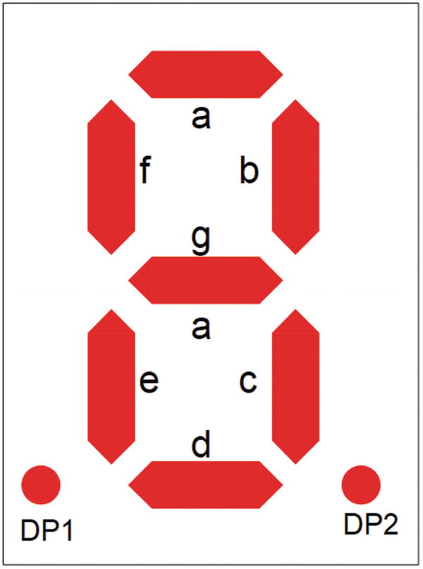
7-segment LED display
There are two types of LED display. The common anode has a single pin for the positive terminal (the anode), whereas the common cathode has a single pin for the negative terminal (the cathode). As these will be driven by a Darlington transistor, they need to be the common anode type. You should check the datasheet for the displays you use to check the pin-out. In my case, I used extra-large displays which have the pins on the side, whereas the smaller displays often have the pins on the top and bottom.
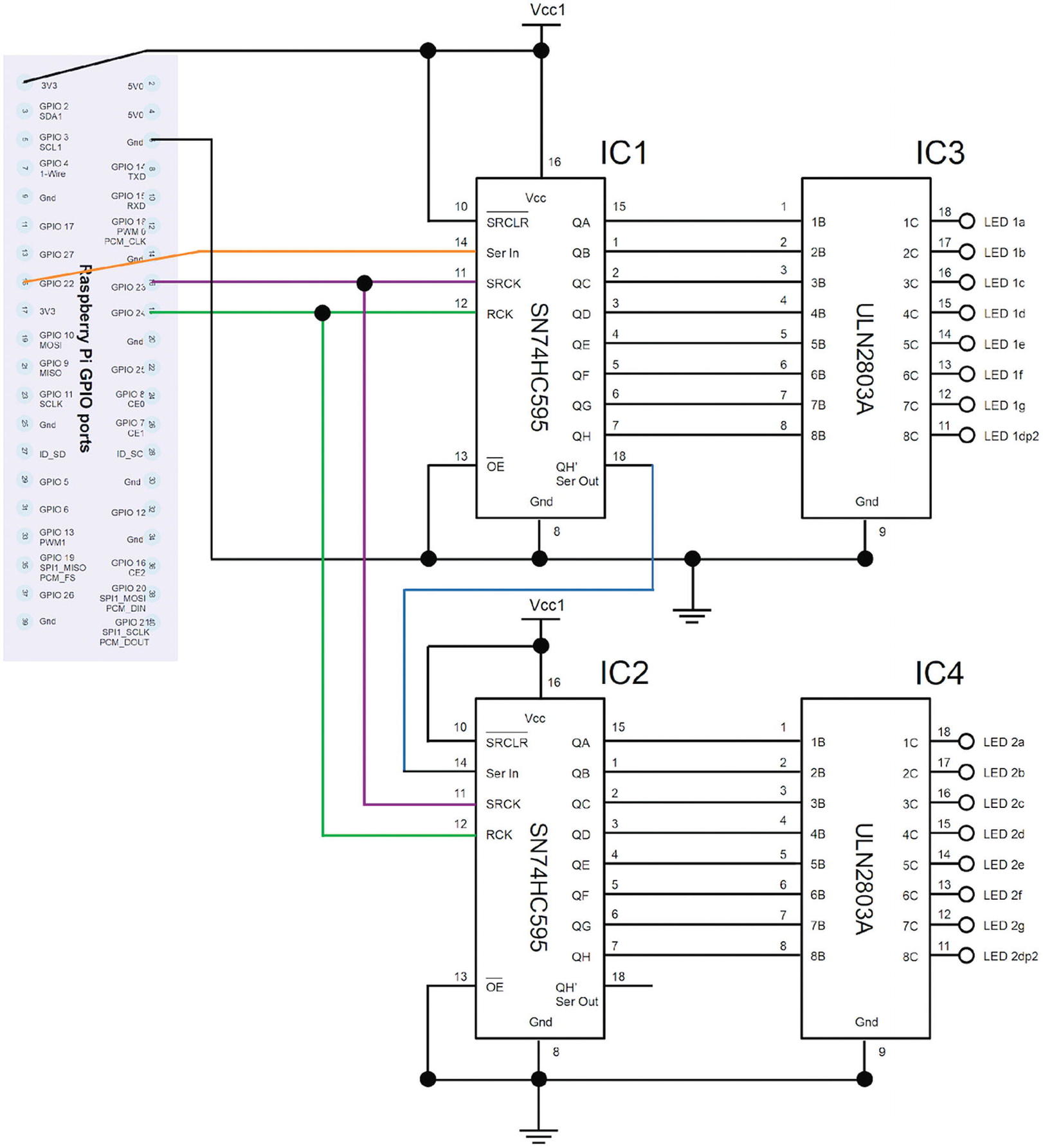
7-segment LED circuit, part one
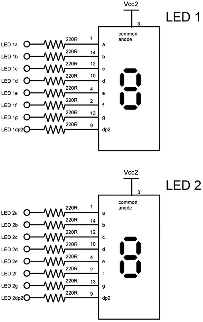
7-segment LED circuit, part two
Looking at the diagrams, there are two ground symbols, two VCC1 power supply labels, and two VCC2 labels. Where the power labels have the same reference, they are connected. This avoids having to have lines crossing the diagram, showing the power supply connection. If a separate power supply is used that is not connected, then that should be labeled different, such that Vcc1 and Vcc2 are different power supplies. In this case, Vcc2 should be a 5V supply; with only two 7-segment displays, these can be taken from the GPIO 5V ports; if more are connected, then it may need an external power supply .
You should be able to follow the rest of the diagrams as they follow the same principles as Figure 11-25, although this uses a different IC, the pins are labeled and numbered differently. The SN74HC595 datasheet uses Q for the outputs, which is fairly common, and then the serial output is marked as QH' which I’ve also labeled as Ser Out. The serial output connects to the serial input of the next shift register IC2, but the same clock signals are used, so both shift registers update at the same time. The datasheet for the Darlington driver IC (ULN2803A) labels the inputs as B and the outputs as C. There is also a common connection which can be used when switching inductive loads (such as motors), but it is not required in this case, so it is left unconnected.
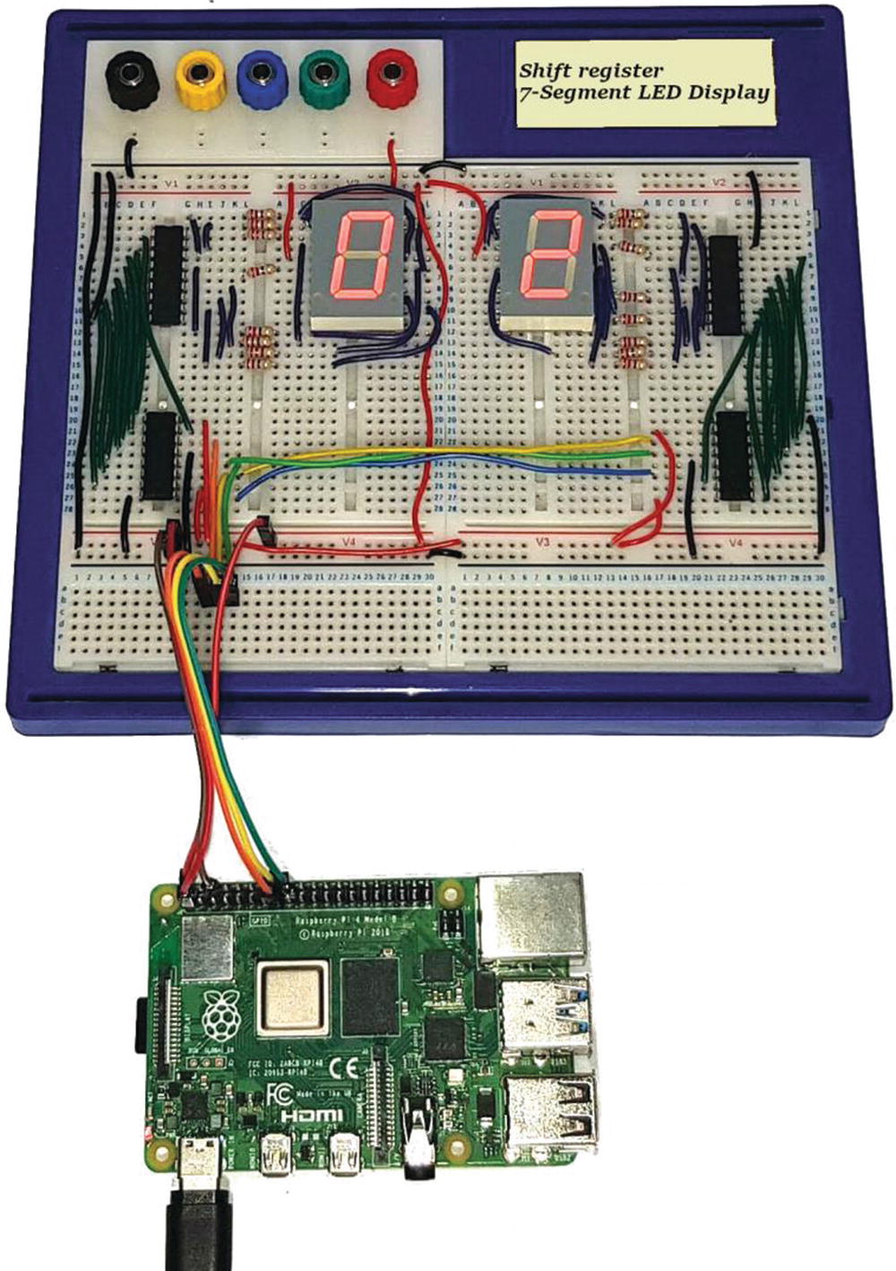
7-segment LED circuit on a breadboard
Shift register demonstration program
To create the number digits in terms of the 7-segment display, a dictionary is created, called number_values. These are the binary bit values to turn on the appropriate LED segments to create the digits from 0 to 9.
The code to send the data to the shift register is similar to the code in Listing 11-1. While using a different type of shift register, the code required to send the serial data is the same. The function shift_byte has an extra optional parameter so that the register_update can be called after both bytes have been sent.
When counting through the values, the number needs to be split into two separate digits for each display which is handled by dividing the value by 10 (using // rounds the number down) and modulo.
The one thing that isn’t included is the decimal point, which can be added by adding a 1 to the value in the number_values dictionary .
Summary
This chapter has shown the basics of digital logic gates and how they can be used to create more complicated combinational logic circuits as well as sequential logic. These are the basic building blocks of logical circuits. This also covers some of the key components that are used in a processor, including additional and registers.
The practical project has shown this can be used to expand the GPIO on the Raspberry Pi by using only three data lines to send serial data to an external shift register. This has been used to drive a bar graph LED display and then a pair of 7-segment LED displays.
The next chapter will look at how circuits can be made more permanent.