
Chapter 12: Prototyping with Breakout Boards
Custom board bring-up is what embedded Linux engineers are called on to do time and time again. A consumer electronics manufacturer wants to build a new device and, more often than not, that device needs to run Linux. The process of assembling the Linux image typically starts before the hardware is ready, and is done using prototypes that are wired together from development and breakout boards. Peripheral I/O pins need to be muxed into device tree bindings for working communications. Only then can the task of coding middleware for an application begin.
Our goal in this chapter is to add a u-blox GPS module to the BeagleBone Black. This requires reading schematics and data sheets so that necessary modifications to the device tree source can be generated using Texas Instruments' SysConfig tool. Next, we will wire up a SparkFun GPS Breakout board to the BeagleBone Black and probe the connected SPI pins with a logic analyzer. Lastly, we will compile and run test code on the BeagleBone Black so that we can receive NMEA sentences from the ZOE-M8Q GPS module over SPI.
Rapid prototyping with real hardware involves lots of trial and error. In this chapter, we will get hands-on experience with soldering and assemble a test bench to study and debug digital signals. We will also revisit device tree source, but this time, we will pay special attention to the pin control configurations and how to utilize them to enable external or onboard peripherals. With a full Debian Linux distribution at our disposal, we can use tools such as git, gcc, pip3, and python3 to develop software directly on the BeagleBone Black.
In this chapter, we will cover the following topics:
- Mapping schematics to the device tree's source
- Prototyping with breakout boards
- Probing SPI signals with a logic analyzer
- Receiving NMEA messages over SPI
Let's get started!
Technical requirements
To follow along with the examples in this chapter, make sure you have the following:
- A Linux-based host system
- A Buildroot 2020.02.9 LTS release
- Etcher for Linux
- A microSD card reader and card
- A USB to TTL 3.3V serial cable
- A BeagleBone Black
- A 5V 1A DC power supply
- An Ethernet cable and port for network connectivity
- A SparkFun model GPS-15193 Breakout
- A row (12 or more pins) of straight breakaway headers
- A soldering iron kit
- Six male to female jumper wires
- A U.FL GNSS antenna
You should have already installed the 2020.02.9 release of Buildroot in Chapter 6, Selecting a Build System. If you have not, then refer to the System requirements section of the The Buildroot user manual (https://buildroot.org/downloads/manual/manual.html) before installing Buildroot on your Linux host according to the instructions
from Chapter 6.
A logic analyzer helps with troubleshooting and understanding SPI communications.
I will be using the Saleae Logic 8 for demonstration purposes. I realize Saleae products are prohibitively expensive ($399 and up), so if you do not already own a Saleae logic analyzer, you can still get through this chapter without one. There are more affordable low-speed alternatives (http://dangerousprototypes.com/docs/Bus_Pirate) that are sufficient for SPI and I2C debugging, but I won't cover them in this book.
All the code for this chapter can be found in the Chapter12 folder of this book's GitHub repository: https://github.com/PacktPublishing/Mastering-Embedded-Linux-Programming-Third-Edition.
Mapping schematics to the device tree's source
Because the BeagleBone Black's Bill Of Materials (BOM), PCB design files, and schematics are all open source, anyone can manufacture a BeagleBone Black as part of their consumer product. Since the BeagleBone Black is intended for development, it contains several components that may not be needed for production, such as an Ethernet cable, a USB port, and a microSD slot. As a dev board, the BeagleBone Black may also be missing one or more peripherals needed for your application such as sensors, an LTE modem, or an OLED display.
The BeagleBone Black is built around Texas Instruments' AM335x, a single core 32-bit ARM Cortex-A8 SoC with dual Programmable Real-Time Units (PRU). There is a more expensive Wireless variant of the BeagleBone Black made by Octavo Systems that swaps out Ethernet with a Wi-Fi and Bluetooth module. The BeagleBone Black Wireless is also open source hardware, but at some point, you may want to design your own custom PCB around the AM335x. Designing a daughterboard (known as a "cape") for the BeagleBone Black is also an option.
For our purposes, we will integrate a u-blox ZOE-M8Q GPS module into a networked device. If you need to transfer lots of packets from a local network to and from the cloud, then running Linux is a sensible choice since it has an extremely mature TCP/IP network stack. The BeagleBone Black's ARM Cortex-A8 CPU meets the requirements (enough addressable RAM and a memory management unit) for running mainstream Linux. This means our product can benefit from security and bug fixes that have been made to the Linux kernel.
In Chapter 11, Interfacing with Device Drivers, we looked at an example of how to bind an Ethernet adapter to a Linux device driver. Binding peripherals is done with device tree source or C structs known as platform data. Over the years, using device tree source has become the preferred means of binding to Linux device drivers, especially on ARM SoCs. For these reasons, the examples in this chapter only involve device tree source. Like U-Boot, compiling device tree source into DTBs is also part of the Linux kernel build process.
Before we can start modifying the device tree source, we need to get acquainted with the schematics for the BeagleBone Black and SparkFun ZOE-M8Q GPS Breakout.
Reading schematics and data sheets
The BeagleBone Black has 2 x 46 pin expansion headers for I/O. These headers include UART, I2C, and SPI communications ports, in addition to numerous GPIOs. Most GPS modules, including ours, can send NMEA data over serial UARTs or I2C. Even though many user space GPS tools, such as gpsd, only work with modules connected via serial, I chose a GPS module with an SPI interface for this project. The BeagleBone Black has two SPI buses available. We only need one of these SPI buses to connect the u-blox ZOE-M8Q.
I chose SPI over UART and I2C for two reasons: UARTs are scarce on many SoCs and needed for things such as Bluetooth and/or a serial console; I2C drivers and hardware can have serious bugs. Some I2C kernel drivers are so poorly implemented that the bus locks up when there are too many connected peripherals talking. The I2C controllers found in Broadcom SoCs, such as the one in the Raspberry Pi 4, are notorious for glitching when peripherals attempt to perform clock stretching.
Here is a map of the pins on the BeagleBone Black's P9 expansion header:
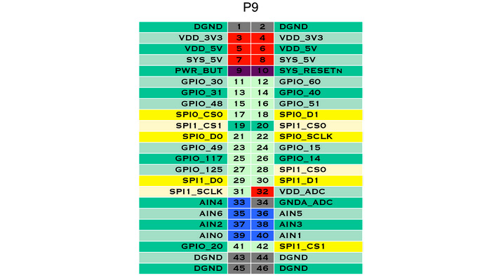
Figure 12.1 – P9 expansion header SPI ports
Pins 17, 18, 21, and 22 are assigned to the SPI0 bus. Pins 19, 20, 28, 29, 30, 31, and 42 are assigned to the SPI1 bus. Notice that pins 42 and 28 duplicate the functionality of pins 19 and 20 for SPI1. We can only utilize one pin for either SPI1_CS1 and SPI1_CS0. Any duplicate pins should be disabled or repurposed. Also, notice that SPI1 has CS0 and CS1 pins, whereas SPI0 only has a CS0 pin. CS stands for chip select. Since each SPI bus is a master-slave interface, pulling a CS signal line low typically selects which peripheral to transmit to on the bus. This kind of negative logic is known as "active low".
Here is a block diagram of the BeagleBone Black's SPI1 bus with two peripherals attached:

Figure 12.2 – SPI1 bus
If we look at the Beagle Bone Black's schematic (https://github.com/beagleboard/beaglebone-black/blob/master/BBB_SCH.pdf), we will
see that four pins (28 to 31) on the P9 expansion header are labeled for SPI1:
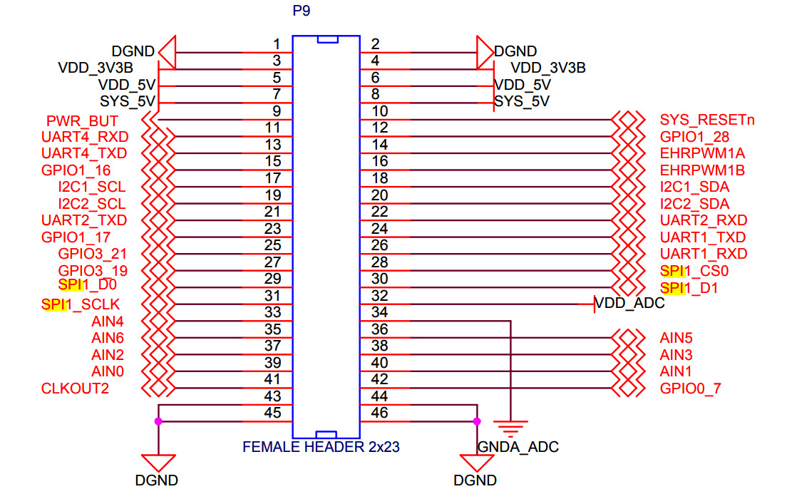
Figure 12.3 – P9 expansion header schematic
The extra SPI1 pins (19, 20, and 42) and all of the SPI0 pins (17, 18, 21, and 22) have been repurposed for I2C1, I2C2, and UART2 on the schematic. This alternate mapping is the result of pin mux configurations defined within the device tree source files. To route the missing SPI signal lines from the AM335x to their respective target pins on the expansion header, the proper pin mux configurations must be applied. Pin muxing can be done at runtime for prototyping but should transition to compile time before the finished hardware arrives.
In addition to CS0, you will notice that the SPI0 bus also has SCLK, D0, and D1 lines. SCLK stands for SPI clock and is always generated by the bus master, which is the AM335x in this case. Data transmitted over the SPI bus is synchronized to this SCLK signal. SPI supports much higher clock frequencies than I2C. The D0 data line corresponds to master in, slave out (MISO). The D1 data line corresponds to master out, slave in (MOSI). While both D0 and D1 can be assigned to either MISO or MOSI in software, we will stick with these default mappings. SPI is a full-duplex interface, which means that both the master and selected slave can send data at the same time.
Here is a block diagram showing the directions of all four SPI signals:

Figure 12.4 – SPI signals
Now, let's turn our attention away from the BeagleBone Black to the ZOE-M8Q. We'll start with the ZOE-M8 series data sheet, which can be downloaded from u-blox's product page at https://www.u-blox.com/en/product/zoe-m8-series. Jump to the section describing SPI. It says that SPI is disabled by default because its pins are shared with the UART and DDC interfaces. To enable SPI on the ZOE-M8Q, we must connect the D_SEL pin to the ground. Pulling down D_SEL converts the two UART and two DDC pins into four SPI pins.
Locate the schematic for the SparkFun ZOE-M8Q GPS Breakout by selecting the "Documents" tab from the product page at https://www.sparkfun.com/products/15193. Searching for the D_SEL pin reveals that it is on the left-hand side of the jumper labeled JP1. Closing the jumper connects D_SEL to GND, thereby enabling SPI:
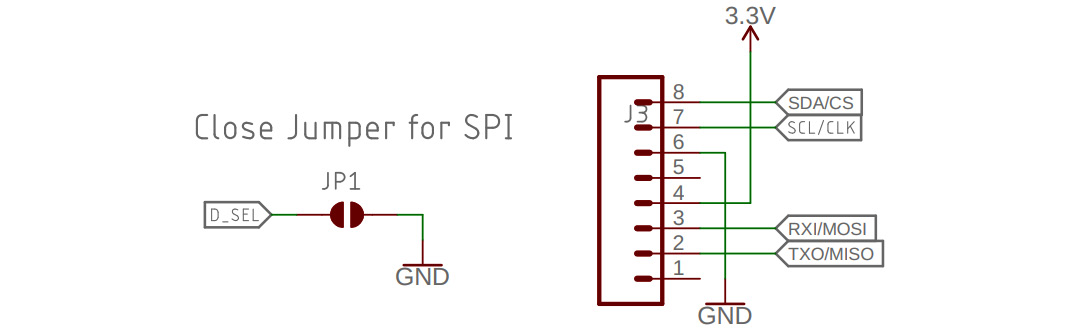
Figure 12.5 – D_SEL jumper and SPI connectors on the GPS breakout
The connectors for the CS, CLK, MOSI, and MISO pins are co-located with 3.3V and GND. Closing the jumper and attaching the headers to the six pins will require some soldering.
Always check the pin ratings when interconnecting chips or modules. The JP2 jumper on the GPS Breakout connects the SCL/CLK and SDA/CS pins to 2.2kΩ pull up resistors. The AM335x data sheet says these output pins are 6mA drivers, so enabling their weak internal pull ups adds 100µA of pull up current. The ZOE-M8Q has an 11kΩ pull up on the same pins, adding 300µA at 3.3V. The 2.2kΩ I2C pull ups on the GPS Breakout add another 1.5mA for a total of 1.9mA of pull up current, which is okay.
Returning to Figure 12.1, notice that the BeagleBone Black supplies 3.3V from pins 3 and 4 of its P9 expansion header. Pins 1 and 2 and 43 to 46 are tied to GND. In addition to connecting the four SPI lines on the GPS Breakout to pins 17, 18, 21, and 22, we will also wire the GPS module's 3.3V and GND to pins 3 and 43 on the BeagleBone Black's P9 expansion header.
Now that we have some idea of how to connect the ZOE-M8Q, let's enable the SPI0 bus on Linux, which is running on the BeagleBone Black. The quickest way to do this is to install a prebuilt Debian image from BeagleBoard.org.
Installing Debian on the BeagleBone Black
BeagleBoard.org provides Debian images for their various dev boards. Debian is
a popular Linux distribution that includes a comprehensive set of open source software packages. It is a massive effort with contributors from all over the world. Building Debian for the various BeagleBoards is unconventional by embedded Linux standards because the process does not rely on cross-compilation. Rather than attempting to build Debian for the BeagleBone Black yourself, simply download a finished image directly from BeagleBoard.org.
To download the Debian Buster IoT microSD card image for the BeagleBone Black, issue the following command:
$ wget https://debian.BeagleBoard.org/images/bone-debian-10.3-iot-armhf-2020-04-06-4gb.img.xz
10.3 was the latest Debian image for AM335x-based BeagleBone boards at the time of writing. The major version number of 10 indicates that 10.3 is a Buster LTS release of Debian. Since Debian 10.0 was originally released on July 6, 2019, it should receive updates for up to 5 years from that date.
Important note
If possible, download version 10.3 (also known as Buster) rather than the latest Debian image from BeagleBoard.org for the exercises in this chapter. The BeagleBone bootloader, kernel, DTBs, and command-line tools are in constant flux, so the instructions may not work with a later Debian release.
Now that we have a Debian image for the BeagleBone Black, let's write it out to a microSD card and boot it. Locate the bone-debian-10.3-iot-armhf-2020-04-06-4gb.img.xz file that you downloaded from BeagleBoard.org from Etcher and write it out to a microSD card. Insert the microSD card into your BeagleBone Black and power it up with a 5V power supply. Next, plug the Ethernet cable from the BeagleBone Black into a free port on your router with an Ethernet cable. When the onboard Ethernet lights start blinking, your BeagleBone Black should be online. Internet access allows us to install packages and fetch code from Git repos from within Debian.
To ssh into the BeagleBone Black from your Linux host, use the following code:
$ ssh [email protected]
Enter temppwd at the debian user's password prompt.
Important note
Many BeagleBone Blacks come with Debian already installed on the onboard flash, so they will still boot, even without a microSD card inserted. If the BeagleBoard.org Debian Buster IoT Image 2020-04-06 message is displayed before the password prompt, then the BeagleBone Black was booted from the Debian 10.3 image on the microSD. If a different Debian release message is displayed before the password prompt, then verify whether or not the microSD card is properly inserted.
Now that we're on the BeagleBone Black, let's look at what SPI interfaces are available.
Enabling spidev
Linux comes with a user space API that provides read() and write() access to
SPI devices. This user space API is known as spidev and is included in the Debian Buster image for the BeagleBone Black. We can confirm this by searching for the
spidev kernel module:
debian@beaglebone:~$ lsmod | grep spi
spidev 20480 0
Now, list the available SPI peripheral addresses:
$ ls /dev/spidev*
/dev/spidev0.0 /dev/spidev0.1 /dev/spidev1.0 /dev/spidev1.1
The /dev/spidev0.0 and /dev/spidev0.1 nodes are on the SPI0 bus, while the
/dev/spidev1.0 and /dev/spidev1.1 nodes are on the SPI1 bus. We only need the SPI0 bus for this project.
U-Boot loads overlays on top of the device tree for the BeagleBone Black. We can select which device tree overlays to load by editing U-Boot's uEnv.txt configuration file:
$ cat /boot/uEnv.txt
#Docs: http://elinux.org/Beagleboard:U-boot_partitioning_layout_2.0
uname_r=4.19.94-ti-r42
.
.
.
###U-Boot Overlays###
###Documentation: http://elinux.org/Beagleboard:BeagleBoneBlack_Debian#U-Boot_Overlays
###Master Enable
enable_uboot_overlays=1
###
.
.
.
###Disable auto loading of virtual capes (emmc/video/wireless/adc)
#disable_uboot_overlay_emmc=1
#disable_uboot_overlay_video=1
#disable_uboot_overlay_audio=1
#disable_uboot_overlay_wireless=1
#disable_uboot_overlay_adc=1
.
.
.
###Cape Universal Enable
enable_uboot_cape_universal=1
Confirm that the enable_uboot_overlays and enable_uboot_cape_universal environment variables are both set to 1. A leading # means that anything after that character in the line is commented out. For this reason, U-Boot ignores all the disable_uboot_overlay_<device>=1 statements shown in the preceding code. This configuration file is applied to U-Boot's environment, so any changes that are saved to /boot/uEnv.txt require a reboot to take effect.
Important note
The audio overlay conflicts with the SPI1 bus on the BeagleBone Black. Uncomment disable_uboot_overlay_audio=1 in /boot/uEnv.txt if you wish to enable communications over SPI1.
To list the device tree overlays U-Boot has loaded, use the following commands:
$ cd /opt/scripts/tools
$ sudo ./version.sh | grep UBOOT
UBOOT: Booted Device-Tree:[am335x-boneblack-uboot-univ.dts]
UBOOT: Loaded Overlay:[AM335X-PRU-RPROC-4-19-TI-00A0]
UBOOT: Loaded Overlay:[BB-ADC-00A0]
UBOOT: Loaded Overlay:[BB-BONE-eMMC1-01-00A0]
UBOOT: Loaded Overlay:[BB-NHDMI-TDA998x-00A0]
The cape universal feature (https://github.com/cdsteinkuehler/beaglebone-universal-io) is unique to the AM3358 version of Debian. It provides access to nearly all of the BeagleBone Black's hardware I/O without us having to modify the device tree source or rebuild the kernel. Different pin mux configurations are activated at runtime using the config-pin command-line tool.
To view all the available pingroups, use the following code:
$ cat /sys/kernel/debug/pinctrl/*pinmux*/pingroups
To view just the SPI pingroups, use the following code:
$ cat /sys/kernel/debug/pinctrl/*pinmux*/pingroups | grep spi
group: pinmux_P9_19_spi_cs_pin
group: pinmux_P9_20_spi_cs_pin
group: pinmux_P9_17_spi_cs_pin
group: pinmux_P9_18_spi_pin
group: pinmux_P9_21_spi_pin
group: pinmux_P9_22_spi_sclk_pin
group: pinmux_P9_30_spi_pin
group: pinmux_P9_42_spi_cs_pin
group: pinmux_P9_42_spi_sclk_pin
Assigning only one pin to a pingroup is unusual. Normally, all the SPI pins (CS, SCLK, D0, and D1) for a bus are muxed together in the same pingroup. We can confirm this strange one-to-one pin to group relationship by looking at the device tree source, which is located inside the /opt/source/dtb-4.19-ti/src/arm directory on the Debian image.
The am335x-boneblack-uboot-univ.dts file in that source directory contains the following includes:
#include "am33xx.dtsi"
#include "am335x-bone-common.dtsi"
#include "am335x-bone-common-univ.dtsi"
That .dts file, together with the three included .dtsi files, define the device tree source. The dtc tool compiles these four source files into a am335x-boneblack-uboot-univ.dtb file. U-Boot also loads device tree overlays on top of this cape universal device tree. These device tree overlays have .dtbo as their file extension.
Here is the pingroup definition for pinmux_P9_17_spi_cs_pin:
P9_17_spi_cs_pin: pinmux_P9_17_spi_cs_pin { pinctrl-single,pins = <
AM33XX_IOPAD(0x095c, PIN_OUTPUT_PULLUP | INPUT_EN | MUX_MODE0) >; };
The pinmux_P9_17_spi_cs_pin group configures pin 17 on the P9 expansion header to act as a CS pin for the SPI0 bus.
Here is the P9_17_pinmux definition, where pinmux_P9_17_spi_cs_pin is referenced:
/* P9_17 (ZCZ ball A16) */
P9_17_pinmux {
compatible = "bone-pinmux-helper";
status = "okay";
pinctrl-names = "default", "gpio", "gpio_pu", "gpio_pd", "gpio_input", "spi_cs", "i2c", "pwm", "pru_uart";
pinctrl-0 = <&P9_17_default_pin>;
pinctrl-1 = <&P9_17_gpio_pin>;
pinctrl-2 = <&P9_17_gpio_pu_pin>;
pinctrl-3 = <&P9_17_gpio_pd_pin>;
pinctrl-4 = <&P9_17_gpio_input_pin>;
pinctrl-5 = <&P9_17_spi_cs_pin>;
pinctrl-6 = <&P9_17_i2c_pin>;
pinctrl-7 = <&P9_17_pwm_pin>;
pinctrl-8 = <&P9_17_pru_uart_pin>;
};
Notice that the pinmux_P9_17_spi_cs_pin group is one of nine different ways P9_17_pinmux can be configured. Since spi_cs is not the default configuration for that pin, the SPI0 bus is initially disabled.
To enable /dev/spidev0.0, run the following config-pin commands:
$ config-pin p9.17 spi_cs
Current mode for P9_17 is: spi_cs
$ config-pin p9.18 spi
Current mode for P9_18 is: spi
$ config-pin p9.21 spi
Current mode for P9_21 is: spi
$ config-pin p9.22 spi_sclk
Current mode for P9_22 is: spi_sclk
Rerun the config-pin commands and prefix them with sudo if you encounter permissions errors. Enter temppwd as password for the debian user. There is a config-spi0.sh script containing these four config-pin commands under
MELP/Chapter12 in the book code archive.
Debian comes with Git installed, so you can clone this book's repository to fetch the archive:
$ git clone https://github.com/PacktPublishing/Mastering-Embedded-Linux-Programming-Third-Edition.git MELP
To enable /dev/spidev0.0 upon booting your BeagleBone Black, use the
following command:
$ MELP/Chapter12/config-spi0.sh
The sudo password is the same as the debian login prompt.
The Linux kernel source comes with a spidev_test program. I have included a copy of this spidev_test.c source file, which I obtained from https://github.com/rm-hull/spidev-test, in this book's code archive, under MELP/Chapter12/spidev-test.
To compile the spidev_test program, use the following commands:
$ cd MELP/Chapter12/spidev-test
$ gcc spidev_test.c -o spidev_test
Now, run the spidev_test program:
$ ./spidev_test -v
spi mode: 0x0
bits per word: 8
max speed: 500000 Hz (500 KHz)
TX | FF FF FF FF FF FF 40 00 00 00 00 95 FF FF FF FF FF FF FF FF FF FF FF FF FF FF FF FF FF FF F0 0D | ......@....?..................?.
RX | 00 00 00 00 00 00 00 00 00 00 00 00 00 00 00 00 00 00 00 00 00 00 00 00 00 00 00 00 00 00 00 00 | ................................
The -v flag is short for --verbose and displays the contents of the TX buffer. This version of the spidev_test program defaults to using the /dev/spidev0.0 device, so no --device argument needs to be passed in to select the SPI0 bus. The full-duplex nature of SPI means that the bus master receives data while transmitting. In this case, the RX buffer contains all zeros, implying that no data was received. In fact, there is no assurance that any of the data in the TX buffer was even sent.
Use a jumper wire to connect pin 18 (SPI0_D1) to pin 21 (SPI0_D0) on the BeagleBone Black's P9 expansion header, as shown here:

Figure 12.6 – SPI0 loopback
The map of the P9 expansion header is oriented so that the header is on the left-hand side of the BeagleBone Black when the USB port is at the bottom. The jumper wire from SPI0_D1 to SPI0_D0 forms a loopback connection by feeding MOSI (master out) into MISO (master in).
Important note
Don't forget to rerun the config-spi0.sh script after rebooting or power cycling your BeagleBone Black to re-enable the /dev/spidev0.0 interface.
Rerun the spidev_test program with your loopback connection in place:
$ ./spidev_test -v
spi mode: 0x0
bits per word: 8
max speed: 500000 Hz (500 KHz)
TX | FF FF FF FF FF FF 40 00 00 00 00 95 FF FF FF FF FF FF FF FF FF FF FF FF FF FF FF FF FF FF F0 0D | ......@.......................
RX | FF FF FF FF FF FF 40 00 00 00 00 95 FF FF FF FF FF FF FF FF FF FF FF FF FF FF FF FF FF FF F0 0D | ......@.......................
The contents of the RX buffer should now match the contents of the TX buffer. We have verified that the /dev/spidev0.0 interface is fully functional. For more on runtime pin muxing, including the origins of the BeagleBone Black's device tree and overlays, I recommend reading https://cdn-learn.adafruit.com/downloads/pdf/introduction-to-the-beaglebone-black-device-tree.pdf.
Customizing the device tree
BeagleBoard.org's cape universal device tree is great for prototyping, but a tool such
as config-pin is not suitable for production. When we ship a consumer device, we know what peripherals are included. There should be no hardware discovery involved
in the boot process aside from reading a model and revision number from an EEPROM. U-Boot can then decide what device tree and overlays to load based on that. Like choosing kernel modules, the contents of the device tree are decisions best made at compile time, not runtime.
Eventually, we will need to customize the device tree source for our custom AM335x board. Most SoC vendors, including Texas Instruments, provide interactive pin mux
tools for generating device tree source. We will use Texas Instruments online SysConfig tool to add a spidev interface to our Nova board. We already customized the device tree for the Nova back in the Porting Linux to a new board section of Chapter 4, Configuring and Building the Kernel, and again in Chapter 6, Selecting a Build System, when we learned how to create a custom BSP for Buildroot. This time, we will add to the am335x-boneblack.dts file instead of just copying it verbatim.
Visit https://dev.ti.com and create an account if you do not already have one. You will need a myTI account to access the online SysConfig tool.
To create a myTI account, follow these steps:
- Click the Login / Register button in the top-right corner of the landing page.
- Fill out the New user form.
- Click the Create account button.
To launch the SysConfig tool, follow these steps:
- Click the Login / Register button in the top-right corner of the landing page.
- Log in by entering your email address and password under Existing myTI user.
- Click on the SysConfig Launch button under Cloud tools.
The Launch button will take you to the SysConfig start page at https://dev.ti.com/sysconfig/#/start, which you can bookmark for quicker access. SysConfig lets us save our working designs to the cloud so that we can revisit them later.
To generate a SPI0 pinmux configuration for the AM335x, follow these steps:
- Select AM335x from the Device menu under Start a new Design.
- Leave the default Part and Package menu selections of Default and ZCE for the AM335x as-is.
- Click the Start button.
- Select SPI from the left sidebar.
- Click the ADD button to add an SPI to your design:

Figure 12.7 – Adding an SPI peripheral
- Rename MySP1 to SPI0 by typing that into the Name field.
- Select SPI0 from the Use Peripheral menu:

Figure 12.8 – Selecting SPI0
- Select Master SPI with 1 chip select from the Use Case menu:

Figure 12.9 – Master SPI with 1 chip select
- Uncheck the CS1 checkbox to remove that item.
- Click on devicetree.dtsi under Generated Files to view the device tree source.
- Select Pull Up from the Pull Up/Down menu for Signals:
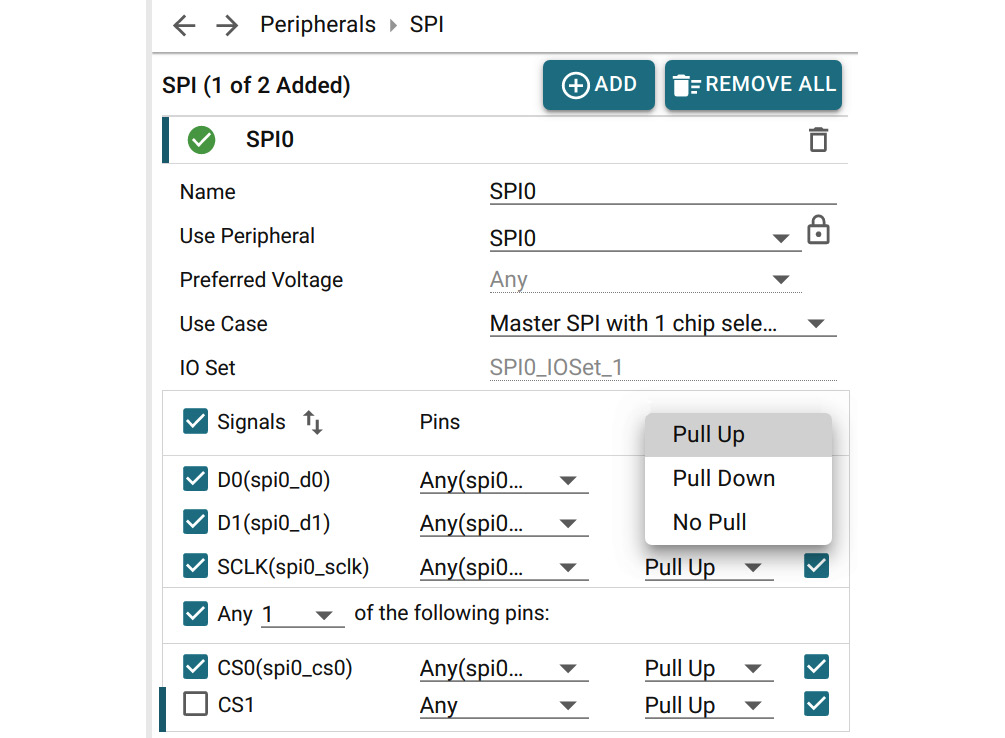
Figure 12.10 – Pull up signals
Notice what this did to the displayed device tree source. All instances of
PIN_INPUT have been replaced with PIN_INPUT_PULLUP. - Uncheck the Rx checkboxes for D1, SCLK, and CS0 since those pins are outputs from the AM335x master, not inputs:

Figure 12.11 – Unchecking the Rx boxes
The D0 pin corresponds to MISO (master in, slave out), so leave Rx checked for that pin. The spi0_sclk, spi0_d1, and spi0_cs0 pins should now be configured as PIN_OUTPUT_PULLUP in the device tree source. Recall that SPI CS signals are usually active low, so a pullup is required to keep that line from floating.
- Click on the floppy icon for devicetree.dtsi to save the device tree source file to your machine.
- Click Save As from the File menu in the top-left corner to save your design.
- Give your design file a descriptive name such as nova.syscfg and click SAVE.
- The contents of the .dtsi file you saved to your machine should look like this:
&am33xx_pinmux {
spi0_pins_default: spi0_pins_default {
pinctrl-single,pins = <
AM33XX_IOPAD(0x950, PIN_OUTPUT_PULLUP | MUX_MODE0) /* (A18) spi0_sclk.spi0_sclk */
AM33XX_IOPAD(0x954, PIN_INPUT_PULLUP | MUX_MODE0) /* (B18) spi0_d0.spi0_d0 */
AM33XX_IOPAD(0x958, PIN_OUTPUT_PULLUP | MUX_MODE0) /* (B17) spi0_d1.spi0_d1 */
AM33XX_IOPAD(0x95c, PIN_OUTPUT_PULLUP | MUX_MODE0) /* (A17) spi0_cs0.spi0_cs0 */
>;
};
[…]
};
I omitted the optional sleep pin settings because we won't need them. If we compare the hexadecimal pin addresses shown in the preceding code with the addresses of those same SPI0 pins in am335x-bone-common-univ.dtsi, we'll see that they match exactly.
The SPI0 pins in am335x-bone-common-univ.dtsi were all configured as follows:
AM33XX_IOPAD(0x095x, PIN_OUTPUT_PULLUP | INPUT_EN | MUX_MODE0)
Use of the INPUT_EN bitmask suggests that all four SPI0 pins in the cape universal device tree are configured as inputs, as well as outputs, when in fact only spi0_ds0 at 0x954 needs to function as an input.
The INPUT_EN bitmask is one of many macros defined in the /opt/source/dtb-4.19-ti/include/dt-bindings/pinctrl/am33xx.h header file, which can be found on the Debian Buster IoT image:
#define PULL_DISABLE (1 << 3)
#define INPUT_EN (1 << 5)
[…]
#define PIN_OUTPUT (PULL_DISABLE)
#define PIN_OUTPUT_PULLUP (PULL_UP)
#define PIN_OUTPUT_PULLDOWN 0
#define PIN_INPUT (INPUT_EN | PULL_DISABLE)
#define PIN_INPUT_PULLUP (INPUT_EN | PULL_UP)
#define PIN_INPUT_PULLDOWN (INPUT_EN)
More TI device tree source macros are defined in the /opt/source/dtb-4.19-ti include/dt-bindings/pinctrl/omap.h header file:
#define OMAP_IOPAD_OFFSET(pa, offset) (((pa) & 0xffff) - (offset))
[…]
#define AM33XX_IOPAD(pa, val) OMAP_IOPAD_OFFSET((pa), 0x0800) (val)
Now that we have properly muxed the SPI0 pins, copy and paste the generated device tree source into our nova.dts file. Once this new spi0_pins_default pingroup has been defined, we can associate that pingroup with the spi0 device node by overriding it, as follows:
&spi0 {
status = "okay";
pinctrl-names = "default";
pinctrl-0 = <&spi0_pins_default>;
[…]
}
The & symbol before the device node name means we are referring to, and thereby modifying, an existing node in the device tree rather than defining a new one.
I have included the finished nova.dts file in this book's code archive, inside the
MELP/Chapter12/buildroot/board/melp/nova directory.
To build a custom Linux image with this device tree for our Nova board, follow these steps:
- Copy MELP/Chapter12/buildroot over your Buildroot installation:
$ cp -a MELP/Chapter12/buildroot/* buildroot
This will either add a nova_defconfig file and board/melp/nova directory or replace the ones from MELP/Chapter06/buildroot.
- cd to the directory where you installed Buildroot:
$ cd buildroot
- Delete all the previous build artifacts:
$ make clean
- Get ready to build an image for our Nova board:
$ make nova_defconfig
- Build the image:
$ make
Once the build has finished, the image is written to a file named output/images/sdcard.img. Use Etcher to write that image to a microSD card. See the Targeting real hardware section of Introducing Buildroot in Chapter 6, Selecting a Build System, to learn how to do this. When Etcher is done flashing, insert the microSD into your BeagleBone Black. There is no SSH daemon included with the root filesystem, so you will need to attach a serial cable to log in.
To log into the BeagleBone Black via a serial console, follow these steps:
- Plug the USB to TTL 3.3V serial cable from your Linux host to the J1 header on the BeagleBone Black. Make sure the black wire on the FTDI end of the cable connects to pin 1 on J1. A serial port should appear on your Linux host as /dev/ttyUSB0.
- Start a suitable terminal program, such as gtkterm, minicom, or picocom, and attach it to the port at 115200 bits per second (bps) with no flow control. gtkterm is probably the easiest to set up and use:
$ gtkterm -p /dev/ttyUSB0 -s 115200
- Apply power to the BeagleBone Black via the 5V barrel connector. You should see U-Boot output, kernel log output, and eventually a login prompt on the serial console.
- Log in as root with no password.
Scroll up or enter dmesg to view the kernel messages during boot. Kernel messages like the following confirm that the spidev0.0 interface was successfully probed via the binding we defined in nova.dts:
[ 1.368869] omap2_mcspi 48030000.spi: registered master spi0
[ 1.369813] spi spi0.0: setup: speed 16000000, sample trailing edge, clk normal
[ 1.369876] spi spi0.0: setup mode 1, 8 bits/w, 16000000 Hz max --> 0
[ 1.372589] omap2_mcspi 48030000.spi: registered child spi0.0
The spi-tools package was included with the root filesystem for testing purposes. The package consists of the spi-config and spi-pipe command-line tools.
Here is the usage for spi-config:
# spi-config -h
usage: spi-config options...
options:
-d --device=<dev> use the given spi-dev character device.
-q --query print the current configuration.
-m --mode=[0-3] use the selected spi mode:
0: low idle level, sample on leading edge,
1: low idle level, sample on trailing edge,
2: high idle level, sample on leading edge,
3: high idle level, sample on trailing edge.
-l --lsb={0,1} LSB first (1) or MSB first (0).
-b --bits=[7...] bits per word.
-s --speed=<int> set the speed in Hz.
-r --spirdy={0,1} consider SPI_RDY signal (1) or ignore it (0).
-w --wait block keeping the file descriptor open to avoid speed reset.
-h --help this screen.
-v --version display the version number.
And here is the usage for spi-pipe:
# spi-pipe -h
usage: spi-pipe options...
options:
-d --device=<dev> use the given spi-dev character device.
-s --speed=<speed> Maximum SPI clock rate (in Hz).
-b --blocksize=<int> transfer block size in byte.
-n --number=<int> number of blocks to transfer (-1 = infinite).
-h --help this screen.
-v --version display the version number.
I won't utilize spi-tools in this chapter, relying instead on spidev-test and a modified version of that same program that I call spidev-read.
We have now gone as far with the device tree source as we are going to go in this book. While DTS is extremely versatile, it can also be very frustrating. The dtc compiler is not very smart, so a lot of device tree source debugging happens at runtime using modprobe and dmesg. Forgetting a pullup or misconfiguring an input as an output when pin muxing can be enough to prevent a device from probing. Wi-Fi/Bluetooth modules with SDIO interfaces are especially challenging to bring up.
With SPI out of the way, it is now time to get up close and personal with the GPS module. We will return to the topic of the generic spidev interface when we have finished wiring up the SparkFun ZOE-M8Q GPS Breakout.
Prototyping with breakout boards
Now that we have SPI working on the BeagleBone Black, let's turn our attention back
to the GPS module. Before we can wire up the SparkFun ZOE-M8Q GPS Breakout, we need to do some soldering. Soldering requires desk space, materials, and a considerable time investment.
To perform the soldering for this project, you will need the following items:
- A soldering iron (adjustable temperature) with a conical tip
- Any one of the following: a silicone car dashboard anti-slip mat, a silicone baking mat, or a ceramic tile
- A fine (0.031-inch gauge) electrical rosin core solder
- A soldering iron stand
- A wet sponge
- A wire cutter
- Safety glasses
- A Helping Hands tool, along with a magnifying glass and an LED light
- An X-Acto #2 knife with a #2 blade or #1 knife with a #11 blade
These items are nice to have but not necessary:
- An insulated silicone soldering mat
- solder wick
- A brass sponge
- Sticky tack or some similar putty-like adhesive
- Dental tools kit
- Needle nose pliers
- Tweezers
Most of these items come bundled together with the SparkFun Beginner Tool Kit, but they can be purchased elsewhere at a lower cost. If you are new to soldering, I also recommend obtaining some scrap PCBs to practice on before operating on the ZOE-M8Q. The holes on the SparkFun GPS Breakout are small and require a steady, delicate touch. A Helping Hands tool with a magnifying glass and alligator clips helps tremendously. Some sticky tack can also hold a breakout board in place on a hard, flat surface while you apply solder. When done, use an X-Acto knife to scrape off any excess sticky tack on or near the contacts.
Even if you are new to electronics, I encourage you to take the plunge and learn to solder. It might take a couple of days of frustration before you get the hang of it, but the satisfaction you get from building your own circuits is well worth it. I recommend reading MightyOhm's free Soldering is Easy comic book by Mitch Altman and Andie Nordgren to get started.
Here are some of my own helpful soldering tips. Wiping your soldering tip with a brass sponge keeps it free from troublesome oxidation. Use an X-Acto knife to scrape off any stray blobs of solder from PCBs. Use a hot iron to melt and play with some solder on your silicone mat to get accustomed to its properties. Lastly, always wear safety glasses when handling hot solder so none gets in your eyes.
Closing the SPI jumper
We located the D_SEL pin on the SparkFun GPS Breakout schematic on the left-hand side of a jumper named JP1. Tying the D_SEL pin to GND on the right-hand side of the jumper switches the ZOE-M8Q from I2C to SPI mode. The two SPI jumper pads already have some solder on them. We need to heat the pads so that we can move that solder around.
Flip the breakout board over to see the jumpers. Notice that the JP1 jumper is labeled SPI on the center left of the board:
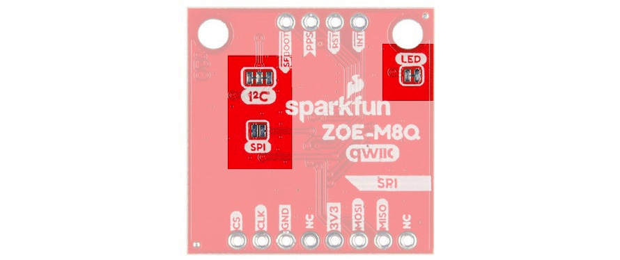
Figure 12.12 – Jumpers
To close the SPI jumper, do the following:
- Plug in and heat your soldering iron to 600 °F.
- Hold the GPS Breakout in place with the alligator clips from your Helping Hands.
- Position your Helping Hands magnifying glass and LED light so that you can clearly see the SPI jumper.
- Place the soldering tip on the left and right pads of the SPI jumper until the solder melts, forming a bridge between the two pads.
- Feel free to add some more solder if necessary.
- Use the tip of your soldering iron to melt and lift off any excess solder from the jumper pads.
Very little solder is needed to close the jumper. If the solder starts to smoke, turn down the temperature of your iron. Once the SPI jumper is closed, serial and I2C communications are disabled on the ZOE-M8Q. The FTDI and I2C pin labels on the top side of the breakout board no longer apply. Use the SPI pin labels on the underside of the board.
Tip
Use the side of the tip (also known as "the sweet spot"), not the very tip of the iron, for best results.
We don't need to repeat this same soldering procedure for the JP2 because the pads
are already bridged on that jumper. JP2 has a separate pad for each of the two 2.2kΩ
I2C pull up resistors. Notice that the JP2 is directly above JP1 and labeled I2C on the breakout board.
Now that the SPI jumper is closed, let's attach the GNSS antenna.
Attaching the GNSS antenna
A ceramic or Molex adhesive GNSS antenna helps the ZOE-M8Q obtain a GPS fix. U.FL connectors are fragile and should be handled with care. Lay the breakout board flat on a hard surface and use a magnifying glass to ensure proper placement of the antenna.
To attach the GNSS antenna to the U.FL connector, follow these steps:
- Align the cable so that the female connector and the end rests evenly across the surface of the male connector on the board.
- Place your finger lightly on top of the stacked connectors to make sure the female connector is not teetering.
- Examine the two stacked connectors from above to make sure they are centered on top of one another.
- Use the center of your finger to press down firmly on the center of the connector, until you feel the two connectors lock together in place.
Now that the antenna is attached, we are ready to attach the SPI header.
Attaching the SPI header
We will use six male to female jumper wires to connect the SparkFun GPS Breakout to
the BeagleBoard Black. The male ends of the jumper wires plug into the P9 expansion header on the BeagleBone Black. The female ends plug into a row of straight breakaway headers that we will solder onto the breakout board. Through-hole soldering with the header pins in place can be difficult, because the pins leave little room in the holes for the solder and tip to slide in. That is why I recommend fine gauge (0.031 inches or smaller) solder for this project.
If you are inexperienced with handling small electronic components, you should first practice soldering some straight breakaway headers onto a scrap PCB. A little extra preparation could save you from damaging and having to replace your expensive ZOE-M8Q GPS module. A proper solder joint should flow around the header pin and fill the hole, forming a volcano-shaped mound. The solder joint needs to touch the metal ring around the hole. Any gaps between the pin and the metal ring will likely result in a bad connection.
To ready the SparkFun GPS Breakout so that you can attach the SPI header, follow
these steps:
- Break off a row of eight header pins.
- Break off a row of four header pins.
- Insert the row of eight through the SPI holes on the underside of the breakout board.
- Insert the row of four through the holes opposite the SPI row on the underside
of the breakout board. This header only serves to keep the board stable while
you're soldering. - Hold the GPS Breakout in place with the alligator clips from your Helping Hands.
- Position your Helping Hands magnifying glass and LED light so that you can clearly see the row of eight FTDI and I2C holes on the top side of the breakout board.
- Plug in and heat your soldering iron to 600 to 650 °F for lead-based solder or 650 to 700 °F for lead-free solder.
Perform the following steps for the six holes on the top side of the breakout board labeled SDA, SCL, GND, 3V3, RXI, and TXO:
- Apply a very small ball of solder to the tip of the hot iron to help prep the joint.
- Heat the header pin and the edge of the metal ring around the hole by touching them with the tip of the iron.
- With the tip of the iron still in place, feed solder into the joint until the hole is filled.
- Pull the melted solder up slowly with the tip of the iron to form a mound.
- Scrape any stray blobs of solder off with an X-Acto knife and use solder wick to remove any accidental solder bridges between holes.
- Clean off any black oxidation that forms on the tip of the iron with either a wet or brass sponge.
Repeat these steps until all six pins have been soldered into their holes. When finished, the top side of the breakout board should look like this:

Figure 12.13 – Solder joints
Note that the jumper wires have already been attached in this photo, even though we haven't gotten to them yet. The two holes labeled NC in the row of eight do not require soldering because they are not connected to anything.
Connecting the SPI jumper wires
Flip the breakout board so that the underside is visible again. By doing this, we can attach the jumper wires. Use a black or gray wire for GND and a red or orange wire for 3V3 to avoid mixing them up and damaging your breakout board. It also helps to use different colors for the other wires so that we don't get the SPI lines confused.
Here are what the female ends of my six jumper wires look like when inserted into the header pins on the underside of the breakout board:
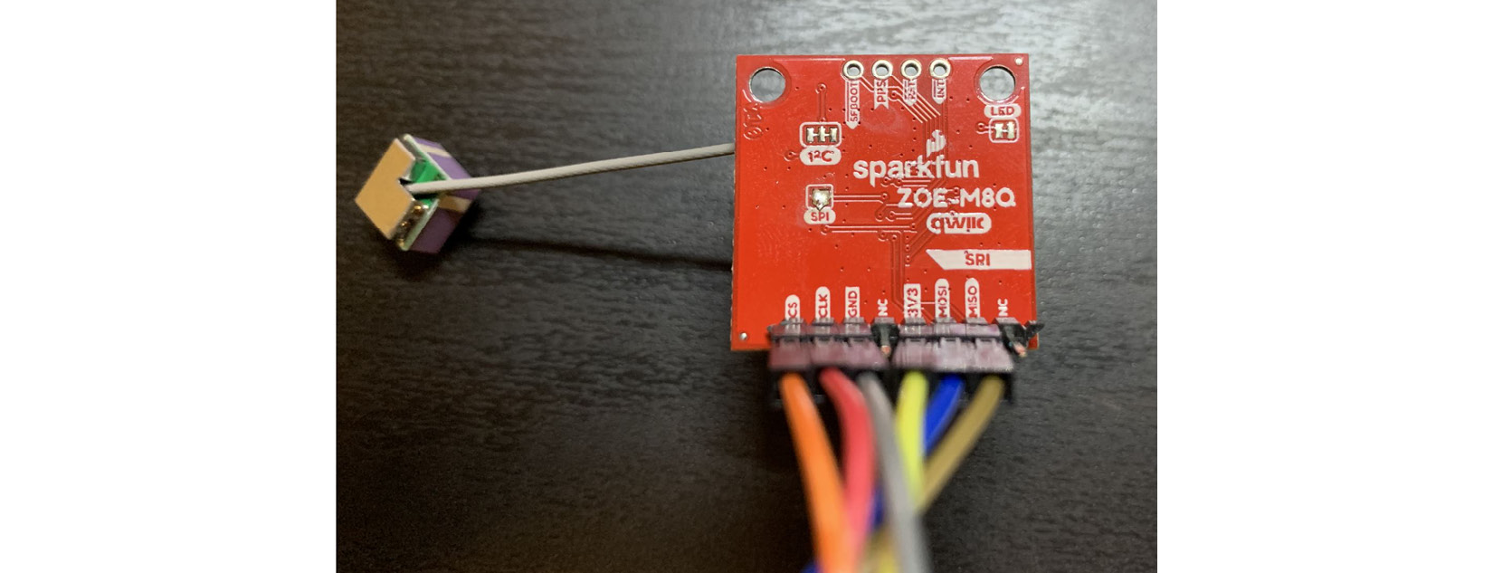
Figure 12.14 – Female ends of the SPI jumper wires
To connect the male ends of the SPI jumper wires to the P9 expansion header on the BeagleBone Black, follow these steps:
- Disconnect the power from the BeagleBone Black.
- Connect the GND wire from the GPS to pin 1 on P9.
- Connect the CS wire from the GPS to pin 17 on P9.
- Connect the CLK wire from the GPS to pin 22 on P9.
- Connect the 3V3 wire from the GPS to pin 3 on P9.
- Connect the MOSI wire from the GPS to pin 18 on P9.
- Connect the MISO wire from the GPS to pin 21 on P9.
As a rule, it is best to connect the GND wire first before any of the other wires. This protects the BeagleBone's I/O lines from any electrostatic discharge that may have built up on the GPS Breakout.
The male ends of the six jumper wires should look like this when connected:

Figure 12.15 – Male ends of the SPI jumper wires
The gray wire connected to pin 1 is GND and the yellow wire connected to pin 3 is 3V3 in my case. The blue wire connected to pin 18 is MOSI on my GPS Breakout. Be careful not to plug the 3V3 wire into either of the VDD_5V pins that are just below the VDD_3V3 pins on P9, as you could destroy your breakout board.
To enable the SPI0 bus on the BeagleBone Black and power up the GPS Breakout, follow these steps:
- Insert the Debian Buster IoT microSD card into your BeagleBone Black.
- Apply power the BeagleBone Black by connecting the 5V power supply.
- Connect your BeagleBone Black to the internet by plugging the board into a port on your router with an Ethernet cable.
- SSH into your BeagleBone Black as debian:
$ ssh [email protected]
- The password is temppwd.
- Navigate to the directory for this chapter, which can be found in this book's archive:
$ cd MELP/Chapter12
- Enable the /dev/spidev0.0 interface:
$ sudo ./config-spi0.sh
Navigate to the spidev-test source directory and run the spidev_test program back-to-back a few times:
debian@beaglebone:~$ cd MELP/Chapter12/spidev-test
$ ./spidev_test
$ ./spidev_test
Pressing the up arrow key saves us from having to retype the previous command. On the second attempt, you should see an NMEA string starting with $GNRMC in the RX buffer:
$ ./spidev_test
spi mode: 0x0
bits per word: 8
max speed: 500000 Hz (500 KHz)
RX | 24 47 4E 52 4D 43 2C 2C 56 2C 2C 2C 2C 2C 2C 2C 2C 2C 2C 4E 2A 34 44 0D 0A 24 47 4E 56 54 47 2C | $GNRMC,,V,,,,,,,,,,N*4D..$GNVTG,
If you see an NMEA sentence in your RX buffer like the one shown here, then everything has gone according to plan. Congratulations! The hardest parts of this project are now over. The rest is "just software", as we like to say in the industry.
If no NMEA sentences (https://en.wikipedia.org/wiki/NMEA_0183) are being received by spidev_test from the GPS module, here are some questions we should ask ourselves:
- Is the cape universal device tree loaded?
Run the version.sh script under /opt/scripts/tools with sudo to
verify this. - Did we run the config-spi0 script without errors?
Rerun config-spi0 with sudo if you encounter permissions errors. Any subsequent No such file or directory errors imply that U-Boot failed
to load the cape universal tree. - Is the power LED on the breakout board lighting up red?
If not, then 3V3 is not connected, so the GPS Breakout is not powering on. If you have a multimeter, then you can use that to determine whether the GPS Breakout is indeed receiving 3.3 V from the BeagleBone Black.
- Is the GND jumper wire from the GPS Breakout connected to pin 1 or 2 on P9?
The GPS Breakout will not operate with proper grounding.
- Are there any loose jumper wires on either end?
All four of the remaining wires (CS, SCLK, MISO, and MOSI) are essential for a working SPI interface.
- Are the MOSI and MISO jumper wires swapped on either end?
Like swapping the TX and RX lines on a UART, this mistake is notoriously easy to make. Color coding our jumper wires helps but labeling them with their names using tape is even better.
- Are the CS and SCLK jumper wires swapped on either end?
Choosing distinct colors for our jumper wires helps us avoid mistakes like these.
If the answers to all these questions check out, then we are now ready to attach the logic analyzer. If you do not have a logic analyzer, then I suggest you reinspect the JP1 jumper and all six solder joints. Make sure the JP1 jumper pads are properly joined. Fill in any gaps between header pins and their surrounding metal rings. Remove any excess solder that could be shorting two adjacent pins together. Add some solder to joints where it may be lacking. Once you are satisfied with this rework, reconnect the jumper wires and reattempt this exercise. With some luck, the results will be better or different this time.
Successful completion of this exercise concludes all the soldering and wiring required for this project. If you are anxious to see the finished product in action, you can skip the next section and jump straight to the Receiving NMEA messages over SPI section. Once you have NMEA data streaming from the GPS module to a terminal window, we can pick up where we left off here and continue learning about SPI signals and digital logic.
Probing SPI signals with a logic analyzer
Even if you succeeded in receiving NMEA from your GPS module, you should attach a logic analyzer such as the Saleae Logic 8 if you have one. Probing the SPI signals helps us understand how the SPI protocol works and acts as a powerful debugging aid when things go wrong. In this section, we will use a Saleae Logic 8 to sample the SPI signals between the BeagleBone Black and ZOE-M8Q. If something is noticeably off with any of the four SPI signals, then a logic analyzer should make that mistake readily apparent.
The Saleae Logic 8 requires a laptop or desktop computer with a USB 2.0 port. The Saleae Logic 1 software is available for Linux, Mac OS X, and Windows. There is an installdriver.sh script that comes with the Linux version of Logic that grants the software permission to access the device. Find that script in the Logic installation's Drivers directory and run it from the command line so that you do not need to launch Logic with sudo every time. Create a shortcut to the Logic executable in the installation folder and place it on your desktop or launch bar for quicker access.
Once the Logic 1 software has been installed on your system, connect to the device with the high-speed USB cable that came with it. Launch the Logic application and wait a moment for the software to connect to and configure the device. When the Logic window says it is Connected at the top, then we are ready to start wiring up our test bench. Press down on the wide end of each test clip with your thumb to extend the grabbers and let go to clasp the pin. Use magnification to read the labels next to the through-holes and ensure the test clips are firmly wrapped around their respective pins.
To assemble a SPI test bench with the Saleae Logic 8, follow these steps:
- Connect the nine-pin cable harness to the logic analyzer. Align the cable harness so that the gray lead points at the ground symbol and the black lead points at the 1 are on the underside of the logic analyzer, as shown here:
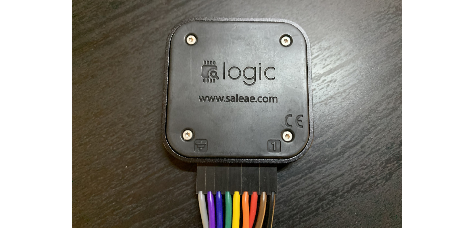
Figure 12.16 – Saleae Logic 8
- Attach test clips to the ends of the gray, orange, red, brown, and black leads. Each test clip has two metal pins that can be inserted into the connector at the end of a lead. Only connect one of these pins to a lead. The black, brown, red, and orange leads correspond to the first four channels in the logic analyzer. The gray lead always connects to GND.
- Disconnect your BeagleBone Black from the 5V power supply so that it is off.
- Pull the female ends of all the jumper wires except for 3V3 from the header pins we soldered onto the GPS Breakout.
- Grab the CS pin on the GPS Breakout with the clip on the orange lead.
- Grab the SCLK pin on the GPS Breakout with the clip on the red lead.
- Grab the GND pin on the GPS Breakout with the clip on the gray lead.
- Skip the NC and 3V3 pins because we are not probing those.
- Grab the MOSI pin on the GPS Breakout with the clip on the black lead.
- Grab the MISO pin on the GPS Breakout with the clip on the brown lead.
- Reconnect the female ends of the jumper wires to the header pins we soldered onto the GPS Breakout. If the jumper wires are already connected, then just slide the female ends up the header pins a bit and attach the test clips. Push the female ends down onto the pins so that they do not slip off easily. The finished assembly should look something like this:

Figure 12.17 – Test clips attached for probing
The yellow jumper wire is 3V3 in my case, so no test clip is attached to it. The blue jumper wire is MOSI, which is probed by the black lead from the logic analyzer.
- Reconnect your BeagleBone Black to the 5V power supply. The GPS Breakout should power up and the onboard power LED should light up red.
To configure the Logic 8 so that it samples on four SPI channels, follow these steps:
- Launch the Logic application and wait for it to connect to the logic analyzer over the USB port.
- Click on the + sign in the Analyzers pane to add an analyzer:

Figure 12.18 – Add Analyzer
- Select SPI from the Add Analyzer pop-up menu.
- Click the Save button in the Analyzer Settings dialog:
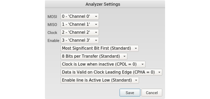
Figure 12.19 – Analyzer Settings
CPOL and CPHA stand for clock polarity and clock phase. A CPOL of 0 means the clock is low when inactive, while a CPOL of 1 means the clock is high when inactive. A CPHA of 0 means data is valid on a clock leading edge, while a CPHA
of 1 means data is valid on a clock trailing edge. Four different SPI modes are available: mode 0 (CPOL = 0, CPHA = 0), mode 1 (CPOL = 0, CPHA = 1), mode 2 (CPOL = 1, CPHA = 1), and mode 3 (CPOL = 1, CPHA = 0). The ZOE-M8Q defaults to SPI mode 0. - Click on the cog button next to Channel 4 on the left sidebar to bring up the Channel Settings pop-up menu:

Figure 12.20 – Hide This Channel
- Select Hide This Channel from the Channel Settings menu.
- Repeat steps 5 and 6 for Channels 5, 6, and 7 so that only Channels 0 to 3 are visible.
- Click on the cog button next to Channel 0 (MOSI) on the left sidebar to bring up the Channel Settings pop-up menu.
- Select 4x from the Channel Settings menu:

Figure 12.21 – Enlarging the channel
- Repeat steps 8 and 9 for Channels 1 to 3 (MISO, CLOCK, and ENABLE) to make those signal graphs larger.
- Click on the button to the right of the cog button for Channel 3 (ENABLE) on the left sidebar to bring up the Trigger Settings pop-up menu. ENABLE corresponds to SPI CS, so we want sampling to start upon receipt of an event from that channel.
- Select the falling edge symbol as the trigger from the Trigger Settings menu:

Figure 12.22 – Selecting the falling edge trigger
- Click on the up/down arrow symbol on the Start button in the top-left corner to set the speed and duration of the sampling.
- Lower the speed to 2 MS/s and set the duration to 50 Milliseconds:

Figure 12.23 – Lowering the speed and duration
As a rule of thumb, the sample rate should be at least as four times as fast as the bandwidth. By this measure, a 1 MHz SPI port requires a minimum sample rate of 4 MS/s. Since spidev_test sets the speed of the SPI port to 500 kHz, then a sample rate of 2 MS/s should be just enough to keep up. Undersampling results in an irregular CLOCK signal. The SPI ports on the BeagleBone Black can operate as fast as 16 MHz. In fact, 16 MHz is the speed spi0.0 defaults to in our custom nova.dts, as shown by dmesg.
To capture an SPI transmission from the BeagleBone Black, hit the Start button in the top-left corner. If the CS signal is behaving correctly, your capture should not start until you run the spidev_test program.
Upon executing spidev_test from the debian@bealglebone terminal, sampling should trigger and a graph similar to the following should appear in the Logic window:

Figure 12.24 – spidev_test transmission
Use the scroll wheel on your mouse to zoom in and out of any interesting segments of the signal graphs. Notice that the ENABLE graph on Channel 3 drops low whenever data is sent by the BeagleBone Black on Channel 0 (MOSI). The CS signal for SPI is normally active low, so the ENABLE graph jumps high when no data is being transferred. If the ENABLE graph stays high, then no more data is sent to the GPS module because that peripheral never gets enabled on the SPI bus.
Here is a closeup of an interesting segment of the MOSI graph on Channel 0:

Figure 12.25 – MOSI segment
Notice that the recorded 0x40 0x00 0x00 0x00 0x00 0x95 byte sequence matches the contents of the default TX buffer for spidev_test. If you see this same byte sequence on Channel 1 instead, then the MOSI and MISO wires could be swapped somewhere in
your circuit.
Here is the tail end of the SPI transfer:
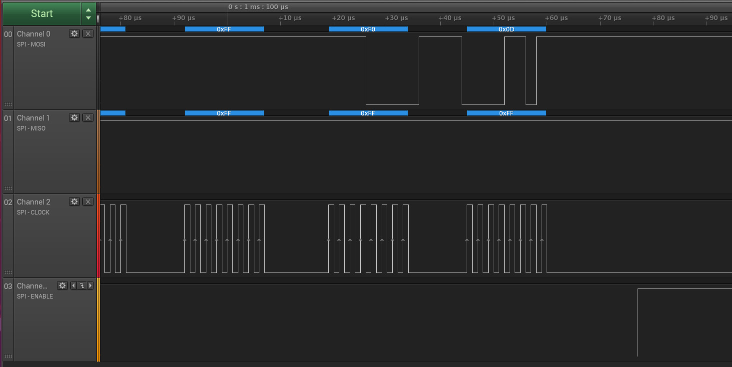
Figure 12.26 – End of spidev_test transmission
Notice that the last two bytes on Channel 0 (MOSI) of this segment are 0xF0 and 0x0D, just like in the default TX buffer. Also, notice that the CLOCK signal on Channel 2 oscillates for a regular number of cycles whenever a byte is transferred. If the CLOCK signal looks irregular, then either the data being sent is getting dropped or garbled or your sample rate isn't fast enough. The signal graph for Channel 1 (MISO) remains high throughout this session since no NMEA message is received from the GPS module on the first SPI transfer.
If the signal on Channel 3 (ENABLE) settles on the logic 0 state, this suggests that the pin being probed was muxed without the PULL_UP bit being set. The PULL_UP bit acts like a pull up resistor holding the line high when the CS signal is inactive, hence the term "active low". If you see what looks like a CLOCK signal on a channel other than 2, then either we probed the wrong pin or swapped SCLK with another wire somewhere. If the signal graphs match the images in the last three figures, then we have succeeded in verifying that SPI is operating as intended.
We now have another powerful tool in our embedded arsenal. Besides SPI, the Logic 8 can also be used to probe and analyze I2C signals. We will use it again in the next section to examine NMEA messages that are received from the GPS module.
Receiving NMEA messages over SPI
NMEA is a data message format supported by most GPS receivers. The ZOE-M8Q outputs NMEA sentences by default. These sentences are ASCII text, starting with the $ character, followed by comma-separated fields. Raw NMEA messages are not always easy to read, so we will use a parser to add helpful annotations to the data fields.
What we want to do is read the stream of NMEA sentences from the ZOE-M8Q out of the /dev/spidev0.0 interface. Since SPI is full-duplex, this also means writing to /dev/spidev0.0, although we can simply write the same 0xFF value over and over again. There is a program called spi-pipe that is designed to do this sort of thing. It is part of the spi-tools package, along with spi-config. Rather than relying on spi-pipe, I chose to modify spidev-test so that it streams the ASCII input from the GPS module to stdout. The source for my spidev-read program can be found in this book's code archive, inside the MELP/Chapter12/spidev-read directory.
To compile the spidev_read program, use the following commands:
debian@beaglebone:~$ cd MELP/Chapter12/spidev-read
$ gcc spidev_read.c -o spidev_read
Now, run the spidev_read program:
$ ./spidev_read
spi mode: 0x0
bits per word: 8
max speed: 500000 Hz (500 KHz)
$GNRMC,,V,,,,,,,,,,N*4D
$GNVTG,,,,,,,,,N*2E
$GNGGA,,,,,,0,00,99.99,,,,,,*56
$GNGSA,A,1,,,,,,,,,,,,,99.99,99.99,99.99*2E
$GNGSA,A,1,,,,,,,,,,,,,99.99,99.99,99.99*2E
$GPGSV,1,1,00*79
$GLGSV,1,1,00*65
$GNGLL,,,,,,V,N*7A
[…]
^C
You should see a spurt of NMEA sentences once every second. Hit Ctrl + C to cancel the stream and return to the command-line prompt.
Let's capture these SPI transfers with the Logic 8:
- Click on the up/down arrow symbol on the Start button in the top-left corner to change the duration of the sampling.
- Set the new duration to 3 seconds.
- Click the Start button in the top-left corner.
- Run the spidev_read program again.
The Logic software should stop capturing after 3 seconds and a graph similar to the following should appear in the Logic window:

Figure 12.27 – spidev_read transmissions
We can clearly see the three spurts of the NMEA sentences on Channel 1 (MISO) precisely 1 second apart from each other.
Zoom in to get a closer look at one of these NMEA sentences:

Figure 12.28 – NMEA sentence segment
Notice that the data on MISO channel now coincides with drops in the ENABLE signal and oscillations on the CLOCK signal. The spidev_read program only writes 0xFF bytes out to MOSI, so there is no activity on Channel 0.
I have included a NMEA parser script written in Python, along with the spidev_read source code. That parse_nmea.py script depends on the pynmea2 library.
To install pynmea2 on the BeagleBone Black, use the following command:
$ pip3 install pynmea2
Looking in indexes: https://pypi.org/simple, https://www.piwheels.org/simple
Collecting pynmea2
Downloading https://files.pythonhosted.org/packages/88/5f/a3d09471582e710b4871e41b0b7792be836d6396a2630dee4c6ef44830e5/pynmea2-1.15.0-py3-none-any.whl
Installing collected packages: pynmea2
Successfully installed pynmea2-1.15.0
To pipe the output of spidev_read into the NMEA parser, use the following command:
$ cd MELP/Chapter12/spidev-read
$ ./spidev_read | ./parse_nmea.py
The parsed NMEA output looks as follows:
<RMC(timestamp=None, status='V', lat='', lat_dir='', lon='', lon_dir='', spd_over_grnd=None, true_course=None, datestamp=None, mag_variation='', mag_var_dir='') data=['N']>
<VTG(true_track=None, true_track_sym='', mag_track=None, mag_track_sym='', spd_over_grnd_kts=None, spd_over_grnd_kts_sym='', spd_over_grnd_kmph=None, spd_over_grnd_kmph_sym='', faa_mode='N')>
<GGA(timestamp=None, lat='', lat_dir='', lon='', lon_dir='', gps_qual=0, num_sats='00', horizontal_dil='99.99', altitude=None, altitude_units='', geo_sep='', geo_sep_units='', age_gps_data='', ref_station_id='')>
<GSA(mode='A', mode_fix_type='1', sv_id01='', sv_id02='', sv_id03='', sv_id04='', sv_id05='', sv_id06='', sv_id07='', sv_id08='', sv_id09='', sv_id10='', sv_id11='', sv_id12='', pdop='99.99', hdop='99.99', vdop='99.99')>
<GSA(mode='A', mode_fix_type='1', sv_id01='', sv_id02='', sv_id03='', sv_id04='', sv_id05='', sv_id06='', sv_id07='', sv_id08='', sv_id09='', sv_id10='', sv_id11='', sv_id12='', pdop='99.99', hdop='99.99', vdop='99.99')>
<GSV(num_messages='1', msg_num='1', num_sv_in_view='00')>
<GSV(num_messages='1', msg_num='1', num_sv_in_view='00')>
<GLL(lat='', lat_dir='', lon='', lon_dir='', timestamp=None, status='V', faa_mode='N')>
[…]
My GPS module was unable to see any satellites or acquire a fixed position. This could be due to any number of reasons, such as choosing the wrong GPS antenna or no clear line-of-sight to the sky. If you are experiencing similar failures, that is okay. RF is complicated and the goal of this chapter was only to prove we could get SPI communications with the GPS module working. Now that we've done that, we can begin to experiment with alternate GPS antennas and more of the ZOE-M8Q's advanced features, such as its support for the much richer UBX message protocol.
With NMEA data now streaming out to the terminal, our project is finished. We succeeded in verifying that the BeagleBone Black can communicate with the ZOE-M8Q over SPI. If you skipped over the Probing SPI signals with a logic analyzer section, now is a good time to resume with that exercise. Like I2C, SPI is supported by most SoCs, so it is worth getting familiar with, especially if your application requires high-speed peripherals.
Summary
In this chapter, we learned how to integrate a peripheral with a popular SoC. To do that, we had to mux pins and modify the device tree source using knowledge gleaned from data sheets and schematics. Without finished hardware in hand, we had to rely on a breakout board and do some soldering so that the part could be wired together with a dev board. Lastly, we learned how to use a logic analyzer to verify and troubleshoot electrical signals. Now that we have working hardware, we can begin to develop our embedded application.
The next two chapters are all about system startup and the different options you have for the init program, from the simple BusyBox init to more complex systems such as System V init, systemd, and BusyBox's runit. Your choice of init program can have a big impact on the user experience of your product, both in terms of boot times and fault tolerance.
Further reading
The following resources provide more information about the topics that were introduced in this chapter:
- Introduction to SPI Interface, by Piyu Dhaker: https://www.analog.com/en/analog-dialogue/articles/introduction-to-spi-interface.html
- Soldering is Easy, by Mitch Altman, Andie Nordgren, and Jeff Keyzer: https://mightyohm.com/blog/2011/04/soldering-is-easy-comic-book
- SparkFun GPS Breakout (ZOE-M8Q and SAM-M8Q) Hookup Guide, by Elias the Sparkiest: https://learn.sparkfun.com/tutorials/sparkfun-gps-breakout-zoe-m8q-and-sam-m8q-hookup-guide