Chapter 8 Epitaxy
8.1 INTRODUCTION
Two ancient Greek words, επl (epi, placed or resting upon) and ταζlζ (taxis, arrangement), are the root of the modern word epitaxy, which refers to extended single-crystal film formation on top of a crystalline substrate. Epitaxy is arguably the most important phenomenon in semiconductor thin-film device technology. Interestingly, however, epitaxy is usually of little concern in most other major thin-film applications, e.g., optical, hard, and protective coatings and films used for recording, storage, and display of information. Although epitaxy was probably first observed to occur in alkali halide crystals more than a century ago, the actual word epitaxy was apparently introduced into the literature by the French mineralogist L. Royer in 1928 (Ref. 1). For many years the phenomenon of epitaxy continued to be of scientific interest to numerous investigators employing vacuum evaporation, sputtering, and electrodeposition methods. A sense of some of this early work on island growth systems, e.g., metal films on alkali halide substrates, was given in Chapter 7.
Actually, a hierarchy of epitaxial effects is exhibited by films and substrates having widely different crystal and electronic structures. The chapter starts by discussing them so that issues related to epitaxial crystallography, interfacial atomic interactions, and film stress and defects can be better appreciated.
Over the past several decades epitaxy has left the laboratory and assumed crucial importance in the processing of electronic and optoelectronic devices. For these purposes, defect-free epitaxial films exhibiting layer growth are essential, and that is where our interest will be centered in this chapter. At the outset two types of epitaxy can be distinguished and each has important scientific and technological implications. Homoepitaxy refers to the case where the film and substrate are the same material. Epitaxial (epi) Si deposited on Si wafers is the most significant example of homoepitaxy. In fact, one of the first steps in the fabrication of integrated circuit transistors is CVD vapor-phase epitaxy of Si on Si (see Section 6.3.2). The reader may well ask why the underlying Si wafer is insufficient; why must single-crystal Si be extended by means of the epi-film layer? The reason is that the epilayer is generally freer of defects, is purer than the wafer substrate, and can be doped independently of it. A dramatic improvement in the yield of early bipolar transistors was the result of incorporating the epi-Si deposition step. The second type of epitaxy is known as heteroepitaxy and refers to the case where films and substrates are composed of different materials, e.g., AlAs deposited on GaAs. Heteroepitaxy is the more common phenomenon and the one the chapter almost exclusively treats. Optoelectronic devices such as light-emitting diodes (LEDs) and lasers utilizing compound semiconductors, are based on heteroepitaxial film structures.
Differences between the two basic types of epitaxy are schematically illustrated in Fig. 8-1. When the epilayer and substrate crystal are identical, the lattice parameters are perfectly matched and there is no interfacial-bond straining. In heteroepitaxy the lattice parameters are necessarily unmatched, and depending on the extent of the mismatch, we can envision three distinct epitaxial regimes. If the lattice mismatch is very small, then the heterojunction interfacial structure is essentially like that for homoepitaxy. However, differences in film and substrate chemistry and coefficient of thermal expansion can strongly influence the electronic properties and perfection of the interface. Small lattice mismatch is universally desired and actually achieved in a number of important applications through careful composition control of the materials involved.
Figure 8-1 Schematic illustration of lattice-matched, strained, and relaxed heteroepitaxial structures. Lattice-matched heteroepitaxy is structurally similar to homoepitaxy.
When the film and substrate lattice parameters differ more substantially, we may imagine the other cases in Fig. 8-1. Either the two lattices strain to accommodate their crystallographic differences or, if this is not possible, dislocation defects form at the interface (relaxed epitaxy). Strained-layer epitaxy generally prevails during the early film formation stages irrespective of crystal structure or mismatch in lattice parameter. It usually occurs between film–substrate pairs composed of dissimilar materials which have the same crystal structure. Lattice parameter differences are generally an order of magnitude larger than in the case of lattice-matched heteroepitaxy. Near the interface the first few film layers strain to match the substrate crystallography; we say that such film growth is pseudomorphic and it gives rise to coherent epilayers. The outstanding examples of strained layer heteroepitaxy are the structures and devices consisting of Gex Si1–x films grown on Si.
In recent years there has been a rising swell of research devoted to both the basic science of epitaxy and its engineering applications. A sampling of this activity includes:
1. Creating new wide-bandgap energy optoelectronic devices, i.e., LEDs and lasers, based on GaInN materials (Ref. 2), and improving the reliability of various photon sources and detectors used in optical communications systems.
2. Fabrication and use of assorted high-speed microelectronic digital, high-frequency, and wireless communications devices composed of Gex Si1–x (Ref. 3) and compound-semiconductor materials (Ref. 4).
3. The dream of creating three-dimensional integrated circuits possessing intrinsically high device-packing densities. Rather than a single level of processed devices, a vertical multifloor structure can be imagined with each level of devices separated from neighboring ones by insulating films (Fig. 8-2). What is crucial is the ability to grow epitaxial semiconductor films on top of or bury them beneath insulating substrates, e.g., Si on SiO2. This will require selective epitaxial growth at existing crystalline Si, and nowhere else, followed by lateral growth across surfaces that are ill suited to epitaxy (Ref. 5).
4. The fabrication of multilayer heterojunction composites. These epitaxial film structures include quantum wells and superlattices. By engineering bandgap structures some remarkable nanoscale quantum electronic and optical devices have emerged (Refs. 6, 7).
5. Deposition of oriented electroceramic films and multilayers for varied purposes, e.g., high-temperature superconductors, magnetic garnets for magnetooptical devices, and ferroelectric films for memory applications (Ref. 8). In the previous chapter the earliest stages of homoepitaxy and island epitaxy were discussed. Building on this prior introduction and emphasizing thicker films, the present chapter has an ambitious agenda. Its purpose is to first present the physical issues related to film crystallography and defect structures that stem from epitaxial deposit–substrate interactions. The major focus of the chapter, however, is layered-film epitaxy of compound semiconductors. Assorted processes to deposit epitaxial compound-semiconductor films and the techniques employed to characterize them will be discussed. Properties of important epitaxial structures and recent applications in electronics and optoelectronics will be stressed throughout.
8.2 MANIFESTATIONS OF EPITAXY
8.2.1 INTRODUCTION
The concept of epitaxy spans a wide latitude of meaning with a hierarchy of structural and physical distinctions. On the one hand what has been called epitaxy can mean a loose structural accommodation between totally different film and substrate materials. For example, graphoepitaxy exemplified by crystalline metals deposited on amorphous substrates lies at one end of the spectrum in this regard; the resulting films are quite defective. Epitaxy can also mean the intimate interaction between materials that are very similar electronically and chemically, possessing the same crystal structure and virtually identical lattice parameters, e.g., certain binary and ternary III–V compound semiconductors; in this case the films are relatively free of defects. This section addresses a variety of fundamental structural, crystallographic and property issues that arise in both common as well as extreme forms of epitaxial behavior.
8.2.2 GRAPHOEPITAXY
This unusual form of epitaxy employs artificial microstructures, fabricated on a substrate surface, to manipulate the nucleation, growth, and orientation of film overlayers. For graphoepitaxy to occur, films must deposit with a given texture, e.g., (100). This means that (100) planes of grains lie parallel to the substrate surface, but their orientation is random and can rotate about the [001] axis. If the grains encounter a substrate pattern raised in relief, e.g., a grating with a period smaller than the grain size, the film will be constrained to perpetuate the original orientation. The effect can be understood by referring to the schematic depiction in Fig. 8-3 of a deposited polycrystalline film with (100) texture. When the substrate surface is either textured with a square (Fig. 8-3b) or triangular (Fig. 8-3c) wave relief, the growing film engulfs the otherwise randomly oriented grains that would form on a flat surface (Fig. 8-3a). Since no crystallographic or even bonding demands are made of the substrate, the latter can even be amorphous; for that matter so can the initial film deposit. Thus, starting with a deposit of amorphous Si (0.5 μm thick) on a fused (amorphous) SiO2 substrate containing a square relief grating (3.8μm spatial period, 0.1μm deep), scanned laser-beam annealing recrystallized and enlarged the resulting Si grains to a size of 100 μm. But there were considerable angular spreads in the [100] direction lying parallel to the grating surface (± 15°) as well as perpendicular to the film surface (± 2.5°).
Figure 8-3 Examples of graphoepitaxy. (a) Polycrystalline film exhibiting a (100) texture deposited on an amorphous substrate. (b) Uniform (100) oriented film deposited on a substrate containing a square-wave relief. (c) Similar (100) oriented film deposited on a substrate containing a triangular-wave structure.
(From Ref. 9. Reprinted with the permission of Dr. D. C. Flanders.)
The phenomenon of graphoepitaxy was described in some detail because it reveals that films can be aligned or oriented even in the presence of a large misfit strain and lack of any apparent bonding between the film and substrate. Machlin (Ref. 10) has persuasively argued that many reports of epitaxy are, in fact, manifestations of graphoepitaxy, where assorted substrate terraces, cleavage steps, and defects are the artificial structures that foster oriented film growth. This is probably true of metal-island epilayer films on alkali halide substrates (Section 7.5.3). In these systems there is generally weak bonding, large lattice misfits, and different film–substrate crystal structures and symmetries.
An important example of graphoepitaxy appears to occur in aluminum interconnect metallizations. Normally, Al grains exhibit (111) texture when deposited on blanket SiO2 surfaces. However, films deposited within confining submicron channels, etched into the surrounding SiO2, are oriented in a bamboo-like grain structure. Such a linear grain array is resistant to electromigration degradation (see Section 11.6.3) because the damage-prone grain boundaries are oriented normal to the current flow. In effect, the Al stripe behaves like a long, thin, sequentially misoriented "single crystal."
8.2.3 HETEROEPITAXY
For the purposes of this chapter we can distinguish between two types of heteroepitaxial systems. The first deals with film–substrate materials that differ structurally, chemically, and electronically from one another, e.g., metal–semiconductor. In contrast there are the (compound) semiconductor–(compound) semiconductor heteroepitaxial structures which share a common crystallography and electronic structure, and often similar chemistry. It is the former case that is treated in this section.
8.2.3.1 Crystallographic Notation
In cases other than graphoepitaxy involving dissimilar materials, the relative orientations between the film and substrate are generally coupled. To understand the epitaxial relationship and the nature of the interfacial structure it is necessary to identify the crystallographic orientations between the film and substrate. Unlike the notation used to describe the two-dimensional surface crystallography in Section 7.2.3.2, the traditional (3-D) Miller indices are employed assuming there is no reconstructed substrate surface. For this purpose the indices of the overgrowth plane are written as (HKL) while those of the parallel substrate plane at the common interface are taken as (hkl). The corresponding parallel directions in the overgrowth and substrate planes, denoted by [UVW] and [uvw], respectively, must also be specified. This tetrad of indices, written by convention as (HKL)//(hkl); [UVW]//[uvw], serves to define the epitaxial geometry. As an example, for parallel epitaxy of Ni on Cu, the notation would read (001)Ni//(001)Cu; [100]Ni//[100]Cu. In this case both planes and directions coincide. For (111)PbTe//(111)MgAl2O4; [211]PbTe//[101]MgAl2O4 the interfacial plane is common but the directions are not. Sometimes, the epitaxial relationships can be predicted on the basis of lattice fitting arguments. Those planes and directions which give the best lattice fit often, but certainly not always, determine the film–substrate orientation.
An important quantity which characterizes epitaxy is the lattice misfit f, which was defined in Section 7.3.4.1 as
where a0(f) and a0(s) refer to the unstrained lattice parameters of film and substrate, respectively. Epitaxy is often a matter of accommodation where elimination of defects requires some bond stretching at the interface by both film and substrate atoms. A compromise is struck, creating a common interfacial lattice parameter. Thus, a positive f implies that the initial layers of the epitaxial film will be stretched in tension while the substrate is compressed. Similarly, a negative f means film compression and an extended substrate.
8.2.3.2 Geometrical Features of Metal/Semiconductor Heteroepitaxy
Metal/semiconductor structures are used for contact applications in all solid-state devices, and although epitaxial films may be desirable they are generally not essential. However, as device and contact dimensions continue to shrink the issue of metal/semiconductor heteroepitaxy assumes a greater urgency; not only does epitaxy affect electrical transport across the junction, but through heteroepitaxy the potential to fabricate three-dimensional silicon circuits is facilitated. Examples of metal- (and metal-silicide–) semiconductor heteroepitaxy are briefly treated in turn.
8.2.3.2.1 Metal/Silicon
We have already noted the sharp, defect-free interface between cobalt silicide (CoSi2) and Si in Fig. 1-4. Similar epitaxial relationships hold between NiSi2 and Si. What makes for excellent epitaxy in the cases of CoSi2 and NiSi2 is the fact that both silicides have cubic CaF2 structures with respective lattice parameters of 5.365 Å and 5.406 Å. These are close to the a0 value for Si, i.e., 5.431 Å, and therefore, the resulting lattice misfit for CoSi2 is simply f = (5.431 Å − 5.365 Å)/5.365 Å = 0.0123. Despite the larger misfit and poorer epitaxy in TiSi2 this metal is currently the contact material of choice in silicon technology because of higher electrical conductivity.
8.2.3.2.2 β-FeSi2/Silicon
Other metal silicide films do not exhibit the same epitaxial quality described above. The much-studied β-FeSi2 is nevertheless interesting because it is a semiconductor and not a metal like other silicides (11). Imposing its low-symmetry orthorhombic structure (a = 9.86 Å, b = 7.79 Å, c = 7.88 Å) on the threefold symmetric (111) Si substrate causes oriented domains of epitaxial βFeSi2 films to form. As shown in Fig. 8-4a the domains are rotated relative to one another. For the indicated overgrowth the epitaxial notation for β-FeSi2 grown on (111) Si is (101)β FeSi2//(111)Si:[010]β-FeSi2//[![]() 10]Si. Similarly, when β-FeSi2 films form on (100) Si substrates, the epitaxial orientation shown in Fig. 8-4b is (100)β-FeSi2//(100)Si:[010]β-FeSi2//[110]Si. If there is no surface reconstruction in these diagrams, calculation of the misfit is relatively straightforward. For example, in the case of the latter, assuming the tetragonal structure approximates the orthorhombic lattice,
10]Si. Similarly, when β-FeSi2 films form on (100) Si substrates, the epitaxial orientation shown in Fig. 8-4b is (100)β-FeSi2//(100)Si:[010]β-FeSi2//[110]Si. If there is no surface reconstruction in these diagrams, calculation of the misfit is relatively straightforward. For example, in the case of the latter, assuming the tetragonal structure approximates the orthorhombic lattice,
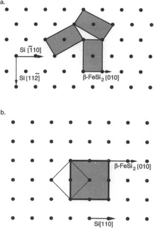
Figure 8-4 Epitaxial relationships between β-FeSi2 and Si. (a) β-FeSi2 (shaded) grown on (111) Si. (b) β-FeSi2 grown on (100) Si.
(From Ref. 11. Reprinted with the permission of the authors.)
8.2.3.2.3 Metal–GaAs Heteroepitaxy
Similar epitaxial relationships between assorted metals and compounds deposited on GaAs and other compound-semiconductor surfaces have also been investigated (Ref. 12). Based on simple geometric matching we can distinguish three different epitaxial arrangements in Fig. 8-5, where the cubic (zinc blende) GaAs substrate (a0(s) = 5.653 Å) is covered by films of materials that also have a cubic crystal structure (e.g., FCC, BCC, CsCl, NaCl).
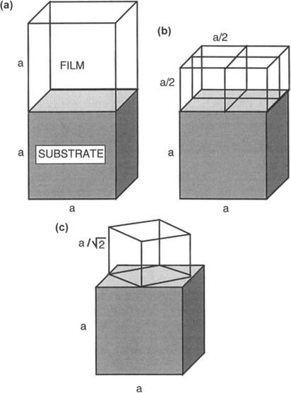
Figure 8-5 Simple epitaxial alignments for cubic films (f) on a cubic substrate (s). (a) a0(f) = a0(s); (b) 2a0(f) = a0(s); (c) 21/2a0(f) = a0(s).
(From Ref. 12. Reprinted with the permission of the author.)
The simplest epitaxial alignment is the cube-on-cube (Fig. 8-5a) where the lattice parameters are equal (a0(s) = a0(f)). For (100) GaAs only the impractical elements Ca (FCC) and Rb (BCC) provide the closest lattice matches. However, rare-earth arsenide (RE-V) films, e.g., ErAs, YbAs, and ErxSc1-x As films, exhibit reasonably good epitaxy. These compounds have the NaCl structure so that the As sublattice is continuous across the (100) interface, thus promoting chemical stability.
There are cases where a0(s) is almost twice a0(f), and such metals are expected to grow epitaxially (Fig. 8-5b). For example, consider the growth of an (110) Fe (BCC) film on (110) GaAs. Because the lattice parameter for Fe is 2.866 Å it appears that two Fe unit cells could be accommodated by one of GaAs. The resulting epitaxial geometry is denoted by
In this system the misfit in the [001] direction is
High-quality epitaxial Fe films have been deposited on GaAs, enabling fundamental studies of ferromagnetism (Ref. 13).
If a0(s) is close to ![]() a0(f) in magnitude, epitaxial deposits are expected to grow in 45° rotated alignment based on lattice-matching arguments (Fig. 8-5c). Candidate metals for such epitaxy include Al and Ag. Epitaxy does occur, but since other film orientations are also observed the situation is more complex. A few monolayers of intervening metal, e.g., Ga for Al, Fe for Ag, sometimes fosters the predicted epitaxy, perhaps by altering surface energies or by providing a growth template.
a0(f) in magnitude, epitaxial deposits are expected to grow in 45° rotated alignment based on lattice-matching arguments (Fig. 8-5c). Candidate metals for such epitaxy include Al and Ag. Epitaxy does occur, but since other film orientations are also observed the situation is more complex. A few monolayers of intervening metal, e.g., Ga for Al, Fe for Ag, sometimes fosters the predicted epitaxy, perhaps by altering surface energies or by providing a growth template.
It is clear that a more complete understanding of dissimilar materials epitaxy must consider issues of interfacial bonding, stress, and thermodynamic stability in addition to simple geometric matching.
8.2.4 TILTED-LAYER EPITAXY
In the various manifestations of epitaxy considered it has been tacitly assumed that the epitaxial films grow with their planes parallel to those of the substrate. But, as schematically illustrated in Fig. 8-6 (top), we have a situation where planes of the epitaxial film are coherently tilted with respect to the substrate planes (Ref. 14). This manifestation of epitaxy occurs on the vicinal surfaces of a miscut substrate. The exposed vicinal planes are slightly misoriented from some major low-index or singular plane. As a result the surface breaks up into an array of low-index terraces of generally variable length terminated by steps whose heights may also vary. When films are deposited on such slightly misoriented (˜ 2–3°) surfaces at high temperatures and/or low fluxes, adatoms are mobile enough relative to their encounter probability and incorporate directly at step edges. In this regime, film growth occurs by step advancement along terraces, i.e., a "step-flow" process. Homoepitaxy of silicon on slightly tilted silicon surfaces, considered in Section 7.5.4.1, essentially proceeds by this mechanism.
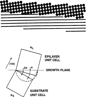
Figure 8-6 (Top) Illustration of tilted-layer epitaxy between film atoms (above) and vicinal planes of substrates (below).
(From Ref. 14.) (Bottom) Geometry of strain relief by tilting lattice-mismatched vicinal heterosystems.
Let us now quantitatively relate the angle of tilt necessary to preserve heteroepitaxial growth of films on a similarly stepped substrate with terraces of constant length. We consider cubic materials under the geometric conditions shown in Fig. 8-6 (bottom) where (100) substrate planes are misoriented from the exposed growth plane by angle α. With a tilt of angle Δα both film and substrate planes will essentially periodically coincide where they intersect at the interface. For a lattice misfit of f, elementary geometry reveals this will happen when
provided the epilayer is fully relaxed (Ref. 15).
8.3 LATTICE MISFIT AND DEFECTS IN EPITAXIAL FILMS
8.3.1 Equilibrium Theory of Lattice Misfit
In this section we explore some implications of lattice misfit with respect to the perfection of epitaxial films. The basic theory which accounts for the elastic/plastic changes in the bilayer was originally proposed by Frank and van der Merwe (Ref. 16). It attempts to account for the accommodation of misfit between two lattices rather than being a theory of epitaxy per se. The theory predicts that any epitaxial layer having a lattice-parameter mismatch with the substrate of less than∼ 9 % would grow pseudomorphically. Initially, very thin films strain elastically to have the same interatomic spacing as the substrate, making the interface coherent with atoms on either side lining up. With increasing film thickness the rising total elastic strain energy will eventually exceed the energy associated with a relaxed structure consisting of an array of misfit dislocations (discussed in Section 8.3.4) separated by wide regions of relatively good fit. At this point the initially strained film ideally decomposes to this relaxed structure where a portion of the misfit is relieved by dislocations. As the film continues to grow, more misfit is relieved until at infinite thickness the elastic strain is totally eliminated. In the case of epitaxial growth without interdiffusion, pseudomorphism exists only up to some critical film thickness dc beyond which dislocations are introduced. Matthews and co-workers (Ref. 17) were the first to derive an expression for dc using an approach that was presented in the first edition of this book.
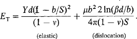
A similar, but perhaps more instructive treatment due to Nix (Ref. 18) is reproduced here. Throughout it is assumed that film and substrate have the same Young’s (Y) modulus and same shear (μ) modulus. The analysis is divided into two film thickness (d) regimes that are depicted in Fig. 8-7.
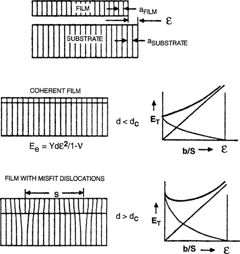
Figure 8-7 Illustration of the Matthews–Blakeslee equilibrium theory of misfit-dislocation formation. (Top) Coherent film is produced when d < dc. (Bottom) Film with misfit dislocations result when d > dc.
(After Ref. 15.) (Reprinted with the permission of the authors.); (From Ref. 18. Reprinted with permission of W. D. Nix.)
1. d < dc. In the early stages of film growth, elastic strain energy Ee (per unit area) increases with d as
see Eq. 1-45 for comparison) where ε is the biaxial elastic strain and ν is Poisson’s ratio. No dislocations are present in the film.
2. d > dc. Now consider the formation of (misfit) dislocations at the film–substrate interface as a means of relieving the elastic strain that develops during further film growth. If the dislocations are assumed to be arrayed in a square grid of side S, the elastic strain in the film is reduced from its initial misfit value (f) to ε = f – b/S. The quantity b/S is proportional to the number of misfit dislocations at the substrate interface and when b/S = f, the film strain vanishes. In essence each dislocation threads the entire film thickness and extends the lateral film length by the Burgers vector magnitude, b. The total strain energy ET (per unit area) is now a sum of the elastic and dislocation energy ETd (per unit area) or
 (8-4)
(8-4)The second term deserves further comment. Theory shows that the energy per unit length of a dislocation is [μb2/4π(1 – v)] ln(R0/b) + Ec, where R0 is a radius about the dislocation where the strain field terminates, and Ec is the dislocation core energy. After incorporating Ec and noting that R0 scales as d, we may substitute R0 = βd, where estimates of constant β range from 0.701 to 2.72. Also, the dislocation length per unit square area of grid is ∼ 2S/S2 or 2/S, and by combining terms, Eq. 8-4 results. Physically the equation indicates that strain energy is a volume energy that increases linearly with film thickness. In contrast, dislocation energy is nearly constant with only a weak logarithmic dependence on d arising from R0.
A plot of each energy contribution vs b/S is shown in Fig. 8-7. The fact that there is a minimum in ET at a nonzero b/S value reveals that the structure is in mechanical equilibrium only if dislocations are present. By minimizing the total energy with respect to dislocation number, i.e., dET/d(b/S) = 0, and evaluating the resulting expression at b/S = 0, the critical film thickness (dc) is determined to be
because μ = Y/2(1 + v). For films thicker than dc, misfit dislocations appear. In the region where dc is approximately a few thousand angstroms, dc is roughly b/2f. This means that the film will be pseudomorphic until the accumulated misfit dcf exceeds about half the unit cell dimension or b/2.
The validity of these ideas has been critically tested on several occasions in Si-based materials. By doping Si wafers with varying amounts of boron, whose atomic size is smaller than that of Si, the lattice parameter of the substrate can be controllably reduced. This affords the opportunity to study defect generation in subsequently deposited epitaxial films under conditions of very small lattice mismatch. As expected, an increase in f resulted in an increase in misfit dislocation density (Ref. 20).
8.3.2 DEFECTS in Gex Si1–x/Si FILMS
Experimentation on Gex Si1–x/Si epitaxial films has enabled the theory to be extended into the regime of large lattice misfits (Ref. 21). The results are shown in Fig. 8-8 where regions of lattice-strained but defect-free (commensurate) epitaxy are distinguished from those of dislocation-relaxed (discommensurate) epitaxy. Nature is kinder to us than the Matthews theory would suggest, and considerably thicker films than dc predicted by Eq. 8-5 can apparently be deposited in practice. The reason is that Gex Si1–x strained-layer films are not in equilibrium. Extended dislocation arrays do not form instantaneously with well-defined spacings; rather, dislocations nucleate individually over an area determined by a width w and unit depth, over which atoms above and below the slip plane are displaced by at least b/2. For isolated screw dislocations, the energy per unit length is approximately equal to ˜ μb2/4π ln d/b; when formed in a film of thickness d, its area energy density is then given by (μb2/ 4πw) ln d/b. By equating this to the elastic energy which drives dislocation nucleation, Bean has shown that
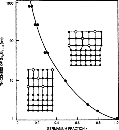
Figure 8-8 Experimentally determined limits for defect-free strained-layer epitaxy of Gex Si1–x on Si. Note that f is proportional to Ge fraction.
(From Ref. 22.)
 (8-6)
(8-6)The solid line of Fig. 8-8 (Ref. 22) represents the excellent fit of this equation to the experimental data for the case where w is arbitrarily chosen to be five [110] lattice spacings or ∼ 19.6 Å. When the lattice misfit becomes large, the spacing between misfit dislocations decreases to the order of only a few lattice spacings. In such a case lattice misfit theory breaks down. There are no longer large areas of good fit separated by narrow regions of poor fit. Rather, poor fit occurs everywhere.
Epitaxial Gex Si1–x films exhibit interesting strain-induced modulations in surface morphology (Ref. 23) that are shown in the TEM cross-sectional image of Fig. 8-9 (top). The surface ripples arise because the film is under compressive stress, a consequence of the fact that lattice parameters of Ge–Si solid-solution alloys necessarily exceed those for Si. As a result the lattice-plane spacing of the film shrinks near the cusplike troughs and expands at the rounded peaks as schematically depicted. A flat surface might be expected to represent the minimum energy configuration. However, when relieval of film strain-energy outweighs the tendency of surface energy (γ) to smooth steps arising from the relaxation distortion, roughening of the surface occurs. Analysis (Ref. 24) reveals that under these conditions the inequality Yε2>4γπ2trms/λ2 holds, where λ and trms are the sinusoidal undulation wavelength and mean height, respectively, and ε is the mismatch strain.
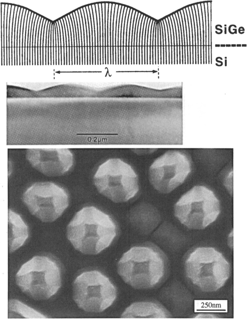
Figure 8-9 (Top) Cross-sectional [100] TEM image of strain-induced surface ripples on an uncapped Ge0.81Si0.19 film and accompanying schematic depiction of the distortion of vertical lattice planes. (Bottom) Scanning electron micrograph top-view of faceted pyramid and dome-shaped islands formed during growth of a 40 nm thick Si0.7Ge0.3 alloy film on (001) Si. Film growth was by UHVCVD (Section 8.6.3.2) at 690°C. The largest islands are 70 nm high.
(After Ref. 23. Reprinted with the permission of the author.); (Courtesy of F. M. Ross, IBM, T.J. Watson Research Center.)
Another manifestation of strain relaxation in compressed epitaxial films is the transition from a planar film to a three-dimensional morphology consisting of pyramidal islands (Ref. 25). This effect is shown in an annealed heteroepitaxial film of Si0.7Ge0.3 at the bottom of Fig. 8-9. The resultant faceted dome-shaped islands produce a surface roughening that is troublesome when fabricating coherently-strained device structures.
8.3.3 TYPES AND SOURCES OF DEFECTS IN EPITAXIAL FILMS
The issues just raised with respect to misfit dislocations and nonplanar surface morphologies are but a part of a larger concern for defects in epitaxial films. Semiconductor wafers are now largely "dislocation free"; in silicon there are fewer than 10 dislocations/cm2 while for GaAs the dislocation density is typically less than 1000/cm2 (Ref. 26). It is well known that dislocations, twins, and stacking faults degrade many device properties by lowering carrier concentrations and mobilities. They create states in the energy gap and serve to reduce the minority carrier lifetime and quantum efficiency of photonic devices. By acting as charge-recombination centers, defects drastically reduce the radiative processes of photon emission or absorption. For these reasons majority-carrier devices can tolerate higher defect levels (e.g., ∼ 105/cm2) than discrete minority-carrier devices (e.g., ∼ 103/cm2). In a decade the Semiconductor Industry Association projects that defect counts in silicon wafers will (must) drop by a factor of between 15 to 20, e.g., 1 oxygen-induced stacking fault/cm2 by 2010 (Ref. 27). Achieving such reductions in increasingly densely packed integrated circuits will require enormous efforts, first to uncover defect origins and then to devise methods for their elimination.
Several categories of defects in epitaxial films are shown schematically in Fig. 8-10 and it is instructive to briefly consider each in turn.
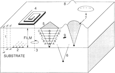
Figure 8-10 Schematic composite of crystal defects in epitaxial films. 1, Threading edge dislocations; 2, interfacial misfit dislocations; 3, threading screw dislocation; 4, growth spiral; 5, stacking fault in film; 6, stacking fault in substrate; 7, oval defect; 8, hillock; 9, precipitate or void.
8.3.3.1 Defect Propagation from Substrate
A classic example of this is the propagation of an emergent screw dislocation spiral from the substrate surface into the growing film. Depositing atoms preferentially seek the accommodating ledge sites of the dislocation spiral staircase. Layers of defect-free film then radiate laterally to cover the substrate. Except for the screw dislocation, an epitaxial layer of otherwise good fit is possible. Occasional substrate dislocations which are present are apparently sources of such dislocations observed in homoepitaxial layers. Gross defects such as grain boundaries and twins are, however, rarely present.
8.3.3.2 Stacking Faults
Stacking faults are crystallographic defects in which the proper order of stacking planes is interrupted. For example, consider the first three atomic planes or layers of a (111) silicon film. Each of these planes may be imagined to be a close-packed array of atomic spheres (Fig. 1-2a), and each successive layer fits into the interstices of the previous layer. Atoms in the second layer (B) have no choice but to nest in one set of interstices of the first (A) layer. It now makes a difference which set of B layer interstices atoms of the third layer choose to lie in. If they lie above neither the A nor the layer atoms, the stacking sequence is ABC, and in a perfect epitaxial film the ABCABCABC, etc, order is preserved. If, however, a plane of atoms is missing from the normal sequence, e.g., ACABCABC, or a plane of atoms has been inserted, e.g., ABCBABCABC, then stacking fault defects are produced. It is established that they propagate from dislocations and oxide precipitates at the substrate interface. Misoriented clusters or nuclei containing stacking faults coalesce with normal nuclei and grow into the film in the manner of an inverted pyramid. Continuing growth causes the characteristic closed triangle shown in Fig. 8-10 to become progressively larger. For (100) growth the stacking faults form squares which can be revealed by appropriate etches. Although stacking faults are a vanishing breed in homoepitaxial Si films their density increases with decreasing growth temperature. In mismatched heteroepitaxial films, e.g., GaAs on Si, stacking faults are common.
Related to stacking faults are the ubiquitous "oval defects" observed during MBE growth (Section 8.6.2) of compound semiconductors. These defects, shown schematically in Fig. 8-10, are faceted growth hillocks which nucleate at the film–substrate interface and nest within the epitaxial layer. They usually contain a polycrystalline core bounded by four {111} stacking-fault planes. With densities of ∼ 10–100 cm−2 and sizes ranging from 1 μm2 to ∼ 30 μm2, these defects are a source of considerable concern. There are a number of possible sources for oval defects in GaAs including carbon contamination from CVD precursors, incomplete desorption of oxides prior to growth, and spitting of Ga and Ga2O from melts.
8.3.3.3 Dislocation Loops from Precipitates, Impurities, or Dopants
This category is self-explanatory. The precipitates and dislocations usually form during cooling and are the result of solid-state reactions subsequent to growth. Films containing high intentional or accidental dopants or impurity levels are susceptible to such defects.
8.3.3.4 Low-Angle Grain Boundaries and Twins
These defects arise from misoriented islands which meet and coalesce. When this happens small-angle grain boundaries or crystallographic twins result. The lattice stacking is effectively mirrored across a twin plane C, i.e.,… BCABCBACB…. Both types of defects may anneal out by dislocation motion if the temperature is high enough. During heteroepitaxial growth Matthews (Ref. 17) has suggested that there is some ambiguity in the exact orientation of small nuclei. He has formulated a rule of thumb that the relaxation of elastic misfit strain causes a variation in the orientation of crystal planes (in radians) roughly equal to the magnitude of the lattice misfit f. Such an effect would naturally give rise to a network of small-angle grain boundaries.
8.3.4 FORMATION OF MISFIT DISLOCATIONS
More attention has probably been lavished on misfit dislocations than any other class of defect in high-performance epitaxial films. Although misfit dislocations lie in planes parallel to the substrate–film interface, they generally originate from threading dislocations (Ref. 28). These pierce through the film, the substrate, or both and lie in crystallographic planes that intersect the interface plane as shown in Fig. 8-11. Consider a threading dislocation arising from the substrate. As it extends into the stressed film the threading component glides or bends in the slip plane. This dislocation segment bends more and more as the film thickens and becomes increasingly stressed. Correspondingly, the threading dislocation portion in the oppositely stressed substrate moves slightly in the opposite direction. Finally, at the critical thickness dc, the film dislocation is able to glide infinitely, leaving behind a stable misfit dislocation at the interface. Threading dislocations can also nucleate from the top surface in the form of a small loop. Film stress expands the loop as the screw dislocation segments (parallel to Burgers vector b) are propelled outward while the edge component (perpendicular to b) glides to the interface and becomes the misfit dislocation. Since large misfits of ∼ 1–2% or more are necessary to nucleate dislocations, it is likely that stress-concentrating particulates, precipitates, or even atomic-scale defects are required to facilitate their formation.
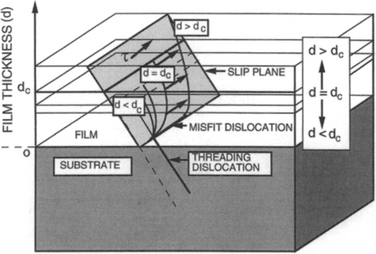
Figure 8-11 A depiction of how stress on thin film plane causes threading dislocation from substrate to form a misfit dislocation when d > dc.
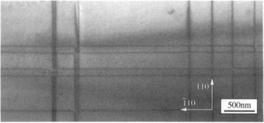
Misfit dislocations have been often observed by transmission electron microscopy. For example, a misfit dislocation array, generated during relaxation of a SiGe alloy film on (100) Si, is shown in Fig. 8-12.
8.3.5 EPITAXIAL DEFECTS IN PERSPECTIVE
In closing, it is appropriate to comment on the various levels of perfection that exist in epitaxial layers. Early epitaxial semiconductor films were judged to be single crystals based on standard X-ray and electron diffraction techniques that are relatively insensitive to slight crystal misorientations. However, subsequent electrical characterization of these films yielded significantly poorer electrical properties than anything imaginable in bulk meltgrown single crystals. In general, thinned slices of bulk crystals were more structurally perfect than epitaxial films of equivalent thickness. This is certainly true of epitaxial films exhibiting island and SK growth and most of the films reported in the older literature. However, many of today’s lattice-matched MBE films, grown under exacting conditions, are indeed structurally perfect when judged by the unambiguous standard of high-resolution TEM lattice imaging. In fact, the crystalline quality of epitaxial films generally exceeds that attainable in bulk grown crystals.
8.4 EPITAXY OF COMPOUND SEMICONDUCTORS
8.4.1 INTRODUCTION
Compound semiconductor films have been grown epitaxially on single-crystal insulators (e.g., Al2O3, CaF2) as well as semiconductor substrates. However, it is the latter case that has attracted the overwhelming bulk of the attention and it will be our primary focus. In the exploitation of compound semiconductors for electronic and optoelectronic devices the creation of epitaxial heterojunctions is crucial (Refs. 29, 30). The term heterojunction refers to the interface between two single-crystal semiconductors of different composition and bandgap energy brought into contact, not differing doping levels of the same semiconductor. To better understand both the structure and electrical properties of these junctions and the devices that make use of them, an introduction to compound-semiconductor materials is an instructive way to start.
8.4.2 COMPOUND-SEMICONDUCTOR MATERIALS
8.4.2.1 Properties
Materials employed for epitaxial electronic and optoelectronic devices are largely drawn from a collection of direct-bandgap III–V semiconductor compounds. Although II–VI and IV–VI semiconductors are used to a much lesser extent, the discussion applies to them as well. Table 8-1 contains a list of important semiconductors together with some of their physical properties. Those that are pertinent to the possibility and quality of epitaxy are semiconductor nature, i.e., direct or indirect bandgap; bandgap energy; lattice constant; and thermal expansion coefficient. The implications of some of these properties on epitaxy/devices are detailed below.
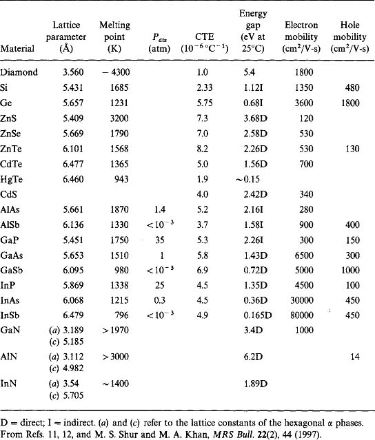
8.4.2.1.1 Direct and Indirect Energy Bandgaps
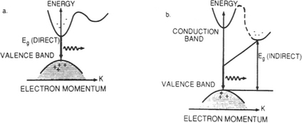
When light is emitted from or absorbed in a semiconductor, energy as well as momentum must be conserved. In a direct-bandgap semiconductor the carrier transitions between the valence and conduction bands occur without change in momentum of the two states involved. In the energymomentum or equivalent energy-wave vector, parabola-like (E vs k) representation of semiconductor bands (Fig. 8-13), emission of light occurs by a vertical electron descent from the minimum conduction band energy level to the maximum vacant level in the valence band. This is what occurs in the direct energy gap materials GaAs and InP. However, in indirect-bandgap semiconductors such as Ge and Si the transition occurs with a change in momentum that is essentially accommodated by excitation of lattice vibrations and heating of the lattice. This makes direct hole–electron recombination with photon emission unlikely. But in direct-bandgap semiconductors such processes are more probable, making them far more efficient (by orders of magnitude) light emitters.
8.4.2.1.2 Bandgap Energy
This important semiconductor property can be understood by considering the variation of the absorption coefficient (α) as a function of photon energy as shown in Fig. 8-14. If light of intensity I0 is incident on a semiconductor surface, the photon intensity at a depth x below the surface is attenuated to I(x), such that
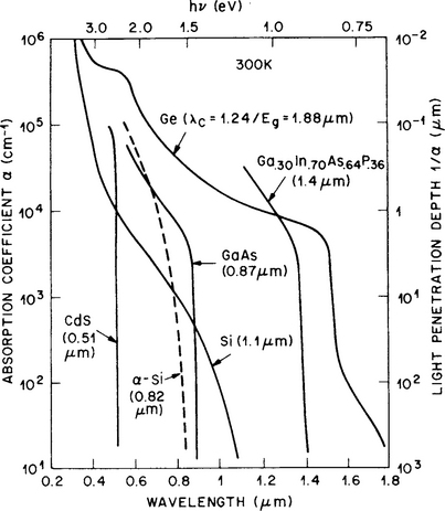
Figure 8-14 Optical absorption coefficients for various semiconductor materials.
(Reprinted with permission from J. Wiley & Sons, S. M. Sze, Semiconductor Devices – Physics and Technology. McGraw-Hill, New York, 1985.)
In all semiconductors α becomes negligible once the wavelength exceeds the cutoff value. This critical wavelength, λc, is related to the bandgap energy Eg by a variant of the well-known relation E = hv or Eg = hc/λc, where h, c, and ν are Planck’s constant and speed and frequency of light, respectively. Alternatively,
For direct-bandgap semiconductors the value of α becomes large on the short-wavelength side of λc, signifying that light is absorbed very close to the surface. For this reason even thin-film layers of GaAs are adequate, for example, in solar cell applications. In Si, on the other hand, α varies more gradually with wavelength less than λc because of the necessity for phonon participation in light absorption/generation processes. Therefore, efficient solar-cell action necessitates thicker layers if indirect-energy-gap semiconductors are employed. In addition to a direct-bandgap semiconductor, photonic device operation generally requires a specific wavelength or value of Eg for light emission or absorption processes.
8.4.2.1.3 Lattice Parameter
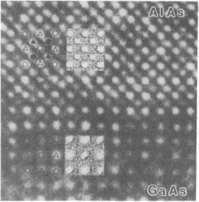
To ensure defect-free interfaces in semiconductor film/substrate heterostructures, it is essential that the lattice parameters (a0) of both be closely matched. For optical devices, lattice mismatches of less than 0.1% are sought. As an example consider GaAs and AlAs with respective a0 values of 5.6532 and 5.6611Å. The lattice mismatch between these compounds is Δa0/a0 or 0.16%. No hint of structural defects at the interface between epitaxial films of these compounds is observed in the lattice image of Fig. 8-15.
8.4.2.1.4 Thermal Expansion Coefficient
To prevent excessive thermal stress from developing at the film–substrate interface during deposition and processing, a match of thermal expansion coefficients is desirable. This condition is largely met in III–V devices based on GaAs, InP, and combinations of these materials.
8.4.2.2 Designing Epitaxial Film–Substrate Combinations
The first three of the semiconductor properties just mentioned converge in the extremely handy graphical representations of Eg vs a0 shown in Figs. 8-16a and 8-16b. These apply, respectively, to the common III–V compound semiconductors (Fig. 8-16a) where Eg < 2 eV, and to the III–V and II–VI materials where Eg >2 eV (Fig. 8-16b), together with their corresponding alloys. Through the use of these figures, the design and selection of complex semiconductor alloys with the desired properties may be visualized. Elements and binary compounds are represented simply as points. Ternary alloys are denoted by lines between constituent binary compounds. When one of the elements is common to both compounds, a continuous range of solid-solution ternary alloys generally forms upon alloying binaries. Thus the line between InP and InAs in Fig. 8-16a represents the collection of InPx As1–x, ternary solution alloys, with x dependent on the proportions mixed. Within the areas outlined by four binary compounds are quaternary alloys. Therefore, the Ga1–x InxAS1–yPy system may be thought of as arising from suitable combinations of GaAs, GaP, InAs, and InP. However, there is no need to start with these four binary compounds when synthesizing a quaternary; it is usually only necessary to control the vapor pressures of the Ga-, In-, As-, and P-bearing species. Furthermore, solid lines represent direct-bandgap ternary compounds while the dashed lines refer to materials with an indirect bandgap.
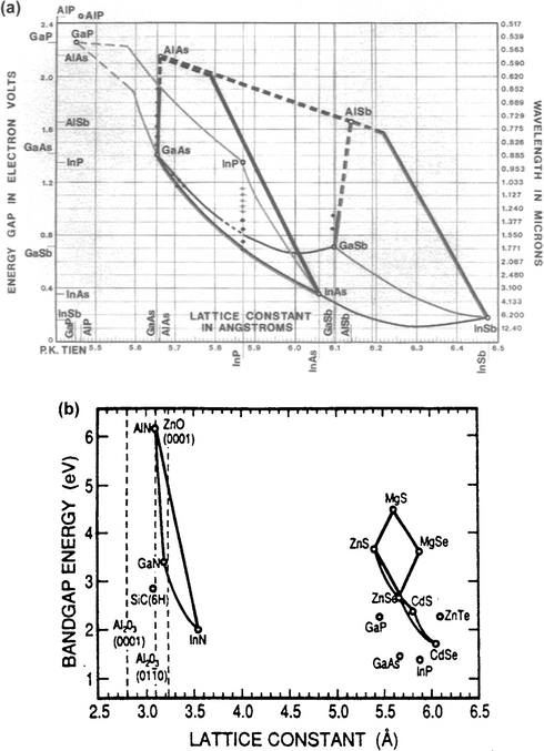
Figure 8-16 Energy gaps and corresponding lattice constants for (a) various III–V compound semiconductors with Eg ![]() 2 eV; (b) various II–VI and III–V compound semiconductors with Eg
2 eV; (b) various II–VI and III–V compound semiconductors with Eg![]() 2 eV. Only data for the hexagonal αAlN, GaN, and InN phases are plotted.
2 eV. Only data for the hexagonal αAlN, GaN, and InN phases are plotted.
(a) (courtesy of P. K. Tien, AT&T Bell Laboratories); (b) (From T. Matsuoka, A. Ohki, T. Ohno, and Y. Kawaguchi, J. Cryst. Growth 138, 727, 1994. Reprinted with the permission of Dr. T. Matsuoka.)
A few examples will illustrate the use of these important diagrams. Suppose it is desired to create semiconductor materials for optoelectronic devices that have an energy gap of 1.0 eV. What are the compositions of some candidate materials and what are their lattice parameters? Extending a horizontal line across Fig. 8-16a at Eg = 1.0 eV (or λ = 1.24 μm) we see that the alloys of the following pairs are crossed: GaAs–InAs; GaAs–GaSb; InP–InAs; AlAs–InAs; AlSb–GaSb; and AlSb–InSb. Although these all appear to be potentially useful, AlSb–GaSb has an indirect bandgap and is disqualified. Even though AlAs and AlSb are also indirect semiconductors, the indicated ternary compositions at 1 eV appear to be direct. Upon alloying these binary compounds we may assume, in the simplest approximation, that the resultant lattice constants and energy gaps of the ternaries are weighted averages of the binary values. As an example, let us determine the composition of the desired InGaAs alloy for which a0 must equal 5.76Å, the value at 1.0 eV. For a linear law of lattice-constant mixtures, i.e., Vegard’s law, a0(InxGa1–xAs) = (x)a0(InAs) + (1 – x)a0(GaAs). Since 5.76 = 6.07x + 5.65(1 – x), x = 0.26, and the predicted alloy has the composition In0.26Ga0.74As. Alternatively, linear averaging of energy gaps gives Eg(InxGa1–xAs) = (x)Eg(InAs) + (1 – x)Eg(GaAs). Thus, 1.0 = 0.36x + 1.43(1 – x) or x = 0.40. To resolve this discrepancy in x, let us consult Table 8-2 for experimental values of direct energy gaps in selected III–V ternary solid solutions. On this basis x is calculated to be 0.40, so the preferred ternary composition is In0.40Ga0.60As.
Table 8-2 Composition Dependence of Direct Energy Gaps in Selected III - V Alloysa
| Alloy | Direct energy gap (eV) | |
|---|---|---|
| Alx Ga1_xAs | 1.424 + 1.455x | (0 < 0.37 < x) |
| Gax In1_x As | 0.36 + 1.064x | |
| Alx In1_xAs | 0.360 + 2.012x + 0.698x2 | |
| GaAsxSb1_x | 0.726 − 0.502x + 1.2x2 | |
| InAsxSb1−x | 0.18 − 0.41x + 0.58x2 | |
| InPx As1_x | 0.360 + 0.891x + 0.101x2 | |
| Alx In1_xSb | 0.172 + 1.621x + 0.43x2 |
a From J. W. Mayer and S. S. Lau, Electronic Materials Science: For Integrated Circuits in Si and GaAs. Macmillan, New York, 1990.
Next, consider the practical problem of fabricating lasers emitting coherent light at 1.0 eV. In these devices, semiconductor films must be deposited on a readily available substrate, e.g., GaAs or InP, and, importantly, be lattice matched to it. Our ternary alloy is lattice-matched to neither GaAs nor InP, and none of the prospective 1 eV materials is lattice-matched to GaAs. A new semiconductor must therefore be found. Calculation using Vegard’s law shows that Ga0.47In0.53As, which is commercially produced for optoelectronic devices, has the same lattice constant as InP; unfortunately, Eg for this ternary alloy is not 1 eV but rather 0.70 eV (from Fig. 8-16a). All is not lost, however, because by alloying Ga0.47In0.53As with InP Eg for the new quaternary GaInAsP alloy can be raised to a value of 1.0 eV, all the while simultaneously maintaining a0 = 5.87Å. To estimate the required stoichiometry we assume Eg(GaInAsP) = (1– x)Eg(Ga0.47In0.53As) + xEg(InP), where x is the fraction of P added. Substituting, 1.0 = (1 – x)0.70 + x1.27 and x = 0.53; therefore, the desired semiconductor film composition is Ga0.22In0.78As0.47P0.53. Growing such a lattice-matched film may not be easy but is certainly not insurmountable.
Other ternary semiconductor properties are similarly altered upon blending binary compounds. For example, the index of refraction n, required for light-guiding properties in lasers, varies as (Ref. 31)
in the AlAs–GaAs system. Thus it is possible to design ternary alloys with a larger Eg and smaller n relative to GaAs, while maintaining an acceptable lattice match for high-quality heterojunctions. These unique combinations of properties have led to the development of a family of injection lasers, light-emitting diodes, and photodiodes in the GaAs–AlAs system and other III–V semiconductors as well.
8.4.3 SCOPE OF DEVICES AND APPLICATIONS
There have been two broad sets of applications based on compound semiconductor epitaxial thin-film structures. The first are optoelectronic devices where generally one, or more commonly, a limited number of heterojunctions is involved. Examples include light-emitting diodes (Fig. 8-17) and lasers (Fig. 8-18). Edge- as well as surface-emitting versions of these light sources exist for assorted purposes, e.g., fiber-optical communications systems, multiaccess optical disks, and optical computing. In solid-state optoelectronic devices, which also include photovoltaics and photodetectors, there are essentially no substitutes for compound semiconductors, i.e., they must stem from III–V, II–VI, or IV–VI materials and their combinations. The operation of the different optoelectronic devices can be simply understood on the basis of Fig. 8-19, which distinguishes among three different phenomena that occur at p–n junctions. In the first (Fig. 8-19a), absorption of a photon with energy of at least Eg results in electron promotion from the valence to conduction band. This is essentially what happens in diode detectors and solar cells, because once there are charge carriers in the conduction band they power and activate electronic circuits. Spontaneous emission of a photon having energy Eg is depicted in Fig. 8-19b.
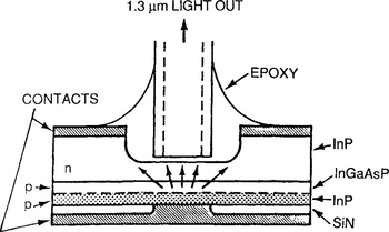
Figure 8-17 Schematic of a surface-emitting InGaAsP (λ = 1.3 μm) light-emitting diode.
(Courtesy N. K. Dutta, AT&T Bell Laboratories.)
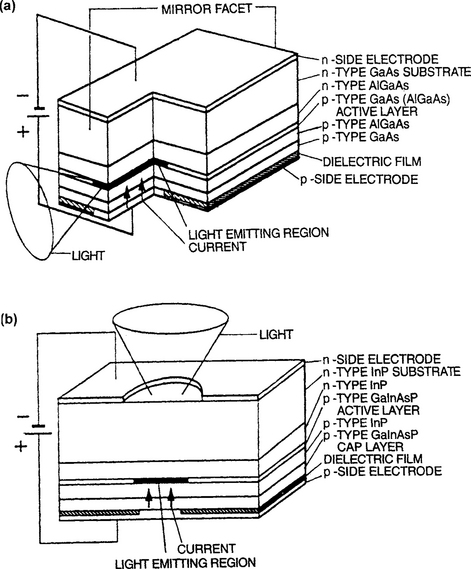
Figure 8-18 Schematic views of basic laser structures. (a) Edge-emitting planar type based on GaAs (or InP). (b) Surface-emitting GaAlAs/GaAs laser prepared by MOCVD.
(From M. Fukuda, Reliability and Degradation of Lasers and LEDs. Reprinted with the permission of Artech House and the author.)
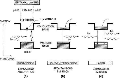
Figure 8-19 Three electron-transition processes between semiconductor valence and conduction bands shown within the context of photonic junction devices. (a) Absorption; (b) spontaneous emission; (c) stimulated emission.
This process arises when current passes through a forward-biased junction, e.g., in a light-emitting diode. Lastly, stimulated emission occurs in lasers whose junctions are also forward-biased (Fig. 8-19c). The existence of an optical cavity and mirrors to confine and enable directed light amplification distinguishes lasers from LEDs. For a more extensive treatment of the physics, characteristics, and operation of photonic devices the reader is referred to the many excellent textbooks (Refs. 30, 32) on the subject.
A second important class of applications for these materials is in analog and digital electronic devices (Ref. 4). Into this category fall assorted discrete diodes and heterojunction transistors as well as integrated-circuit combinations for use in computer circuits and high-frequency communications systems. Although present computer technology is based almost exclusively on silicon devices and integrated circuits, there are other interesting high-speed electronics applications where compound semiconductor devices are indispensable. As examples we cite wireless communications of all kinds at RF and particularly microwave (˜ 1 GHz to 1000 GHz) frequencies. They employ analog as well as digital devices and circuits made of these materials for such diverse purposes as mobile communications, satellite-based voice and data systems, and computer networking applications. The high charge-carrier mobilities evident in Table 8-1 are central to these applications. There are also advantages in using heterojunctions. For example, in transistor heterostructures with an emitter having a wider bandgap relative to both base and collector, there is a barrier to reverse injection of minority carriers, and this raises the gain/efficiency ratio of the device.
In addition to these examples of "traditional" heterojunctions, an exciting thrust of compound semiconductor epitaxy deals with superlattices or layered stacks of films. These structures not only have interesting scientific implications, but have been incorporated in assorted electronic and photonic devices where their unique properties have improved or extended traditional performance levels.
For reasons of interest and book balance (there is already much coverage of electronic devices), the subsequent discussion will focus on optical devices.
8.4.4 LIGHTING THE IR TO VISIBLE SPECTRUM WITH COMPOUND SEMICONDUCTORS
The development of materials and devices for operation in the spectral domain extending from the visible to the infrared has been one of the great triumphs of solid-state science and engineering in the past three decades (Ref. 33). High-brightness light-emitting diode sources have been a particular quest and the record of achievement based on quantum efficiencies, i.e., the number of photons generated per electron–hole pair, has been impressive. For example, the following quantum efficiencies have been recorded for LEDs in the visible region: 17% for red (0.629 μm); 11.5% for orange (0.604 μm); 6.3% for green; and 9% for blue. Some sample materials issues and applications are provided next to provide a sense of this technological odyssey, which has now made blue lasers and white LEDs a reality.
8.4.4.1 Optical Communications
Optical communication systems transmit information optically through fibers. This is done by converting the initial electronic signals into light pulses employing laser or light-emitting diode light sources. The light launched at one end of an optical fiber is confined to the fiber core and propagates along it over long distances. At the other end of the system the light pulses are detected by photodiodes and converted back into electronic signals, which, in telephone applications, finally generate sound. In such a system it is crucial to transmit the light with minimum attenuation or low optical loss. Great efforts have been made to use the lowest-loss fiber possible and minimize loss at both the source and detector ends. If optical losses are high, it means that the optical signals must be reamplified with additional, costly repeater stations. The magnitude of the problem can be appreciated when transoceanic communications systems are involved. In silica-based fibers it has been found that minimum transmission losses occur at a wavelength in the range 1.3–1.55 μm The necessity to operate within this IR-wavelength window bears directly on the choice of suitable semiconductors and epitaxial deposition technology required to fabricate the required sources and detectors.
Reference to Table 8-1 shows that InP is transparent to 1.3–1.55 μm light. This means that InP wafers can serve both as a substrate on which epitaxial films can be grown and as a mechanical support facilitating the coupling of fibers to devices (Fig. 8-17). As we have seen earlier a very close lattice match to InP (a0 = 5.869Å) can be effected by alloying Ga0.47In0.53As and InP. In this way high-performance lasers based on the lattice-matched GaInAsP/InP system have emerged for optical communications use.
8.4.4.2 Light-Emitting Semiconductor Devices
Bright visible-light-emitting devices with λ > 0.5 μm have been available for well over 30 years. The ubiquitous red lasers and light-emitting diodes are based on epitaxial AlGaAs on GaAs, while orange, yellow, and green LEDs are fabricated from indirect bandgap materials, e.g., GaAsP doped with nitrogen. However, practical sources for the violet-blue-green end of the spectrum, i.e., 0.4–0.5 μm have been notably slow in appearing. They require semiconductors with wide energy bandgaps ranging from somewhat below 2.5 to 3 eV and greater. Table 8-1 reveals that all compound semiconductor classes have potential candidate materials in this Eg range, e.g., (II–VI) ZnS, ZnSe, and ZnTe; (III–V or III–N) GaN, AlN, and InN; and (IV–VI) SiC, an indirect semiconductor. Despite much research and development over the years, particularly in II–VI materials (Ref. 34), devices derived from them were not commercialized even though sizable wafers of ZnS, ZnSe, ZnTe, and SiC have been available for some time (Ref. 35). Two major obstacles to the fabrication of II–VI and III–N diode devices have been the difficulty in doping these materials p-type, and the unacceptably large dislocation and stacking fault densities at heteroepitaxial interfaces. The former has limited junction formation while the latter has led to short-lived devices. With advances in p-doping (˜ 1018/cm3 in ZnSe) coupled with a reduction in defect density (to ∼ 105/cm2) due to epitaxial growth first on GaAs (where f = 0.25%) and then on ZnSe wafers, device performance improved (laser lifetimes of ∼ 1000 h); however, it still fell short of what was demanded. Blue-light device prospects for the wurtzite or hexagonal III–N materials appeared to be even more dim. For example, in the case of GaN the substrate of choice is sapphire (Al2O3) but the lattice mismatch of 14% has led to dislocation densities of ∼ 1010/cm2. In comparison, defect densities of less than ∼ 103/cm2 are typical in lattice-matched III–V devices grown on GaAs and InP.
8.4.4.3 GaN Light-Emitting Semiconductor Devices
The situation just described prevailed until 1993 when Nichia Chemical Industries, a small family-owned business in Japan, astonished the world by demonstrating a very bright blue GaN LED (Ref. 36). This revolutionary advance as well as subsequent ones based on it were spearheaded by S. Nakamura and enabled Nichia to leap ahead of Western efforts in this area (Refs. 37-40). Two key discoveries contributed to this progress. First, satisfactory p-type doping was achieved using Mg. Secondly, a compliant, recrystallized amorphous buffer film of GaN on top of the sapphire substrate reduced the harmful effects of dislocations and lattice and thermal expansion coefficient mismatches. This enabled device-quality epitaxial GaN layers to be grown by MOCVD methods, despite initially high dislocation densities (Ref. 2).
Today, highly efficient UV, blue, and green InGaN LEDs have been fabricated with (external) quantum efficiencies of 7.5% at 0.371 μm (UV), 11.2% at 0.468 μm (blue), and 11.6% at 0.520 μm (green). Some of these blue-light sources have brightnesses of more than 1000 mcd and are comparable to superbright red LEDs; they are more than a hundred times brighter than SiC blue LEDs. There are many actual as well as potential applications for this new generation of light sources. The largest LEDdisplay sky screen in the world, located in Tianjin, China, measures 40 meters in length and 14 meters in height and contains some 680,000 blue and 1,700,000 green LEDs. Traffic lights composed of blue LED sources have already appeared.
An important recent advance has been the development of long-lived InGaN blue-light lasers (Ref. 40) such as that shown in Fig. 8-20. Laser lifetimes critically depend on the dislocation density in the active diode region, and this has been dramatically reduced by fabricating devices on epitaxial layers that are seeded and grown over a buffer layer (see Section 8.5.2.2). Upon commercialization of blue lasers, an important application promises to be optical storage for memories. Since information storage densities vary as the inverse square of the wavelength of light used, increases by a factor of about 4 may be anticipated relative to the present red AlInGaP lasers. A big prize would be an LED or laser-based replacement for the incandescent lamp. For more detailed information the reader should consult the now extensive literature on this subject.
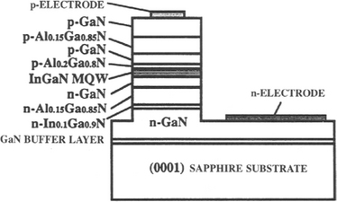
Figure 8-20 Structure of the first InGaN multiquantum-well laser diode.
(From Ref. 40. Reprinted with the permission of the author.)
8.5 HIGH-TEMPERATURE METHODS FOR DEPOSITING EPITAXIAL SEMICONDUCTOR FILMS
8.5.1 SCOPE
In both this and the next section methods for depositing epitaxial semiconductor films will be described. For convenience of organization, Section 8.5 focuses primarily on elevated-temperature processes where chemistry and chemical equilibria play important roles. Thus, liquid-phase epitaxy involving semiconductor melts, and CVD methods are primarily stressed here. On the other hand, generally lower-temperature epitaxial deposition processes, characterized perhaps more in physical than chemical terms, are emphasized in Section 8.6. The prime example of this case is molecular beam epitaxy (MBE). Nevertheless, a stark division into two categories is somewhat arbitrary because deposition processes overlap and exist in hybrid combinations. For example, MOCVD, a relatively low-temperature process, is treated in this section, but MOMBE, which is essentially MBE but employs MOCVD precursors, is deferred to the next. Throughout, distinctions between these processes will be raised, and their applications and relative merits stressed.
8.5.2 EPITAXIAL FILMS FROM MELTS
8.5.2.1 Liquid-Phase Epitaxy
In liquid-phase epitaxy (LPE) melts rather than vapors are in contact with the growing films and substrates. Introduced in the early 1960s LPE is still widely used to produce compound-semiconductor devices. For example, of commercially produced devices presently over 40% are light-emitting diodes, and of these almost 50% are LPE-grown GaP devices; another 20% are LPE-grown AlGaAs/GaAs LEDs (Ref. 41). However, for greater layer uniformity and atomic abruptness, LPE has been supplanted by various vapor-phase epitaxy methods, notably MOCVD. LPE involves the precipitation of a crystalline film from a supersaturated melt onto a substrate that serves as both the template for epitaxy and the physical support for the heterostructure. The process can be understood by referring to the GaAs binary phase diagram (Fig. 1-15). Consider a Ga-rich melt containing 10 at.% As. When heated above ∼ 920°C all of the As dissolves. If the melt is cooled below the liquidus temperature into the two-phase field, it becomes supersaturated with respect to As. Only a melt of lower than the original As content can now be in equilibrium with GaAs. The excess As is, therefore, rejected from solution in the form of GaAs which grows epitaxially on a suitably placed substrate. Readers will appreciate that the crystals they grew as children from supersaturated aqueous solutions essentially formed by this mechanism.
Through control of cooling rates, different kinetics of layer growth apply. For example, the melt temperature can either be lowered continuously together with the substrate (equilibrium cooling) or separately reduced some 5–20°C and then brought into contact with the substrate at the lower temperature (step cooling). Theory backed by experiment has demonstrated that the epitaxial layer thickness increases with time as t3/2 for equilibrium cooling and as t1/2 for step cooling (Ref. 29). Correspondingly, the growth rates or time derivatives vary as t1/2 and t−1/2, respectively. These diffusion-controlled kinetics respectively indicate either an increasing or decreasing film growth rate with time depending on mechanism. Typical growth rates range from ∼ 0.1 to 1 μm per minute. A detailed analysis of LPE is extremely complicated in ternary systems because it requires knowledge of thermodynamic equilibria between solids and solutions, nucleation and interface attachment kinetics, solute partitioning, diffusion, and heat transfer. LPE offers several advantages over other epitaxial deposition methods, including low-cost apparatus capable of yielding films of controlled composition and thickness, with lower dislocation densities than the parent substrates.
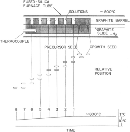
To grow multiple GaAs/AlGaAs heterostructures, the seed substrate is sequentially translated past a series of crucibles holding melts containing various amounts of Ga and As together with such dopants as Zn, Ge, Sn, and Se as shown in Fig. 8-21. Each film grown requires a separate melt. Growth is typically carried out at temperatures of ∼ 800°C with maximum cooling rates of a few degrees Celsius per minute. Limitations of LPE growth include poor thickness uniformity and rough surface morphology, particularly in thin layers. The CVD and MBE techniques are distinctly superior to LPE in these regards.
Although semiconductor LPE applications have been stressed here, the technique is also widely practiced to prepare epitaxial films of niobates and garnets.
8.5.2.2 Seeded Lateral Epitaxial Film Growth over Insulators
The methods we describe here briefly have been successfully implemented in Si but not in GaAs or other compound semiconductors. Inclusion of this subject here is suggested by the use of melts. Technological needs for three-dimensional integrated circuits and isolation of high-voltage devices have spurred the development of techniques to grow epitaxial Si layers over such insulators as SiO2 or sapphire. The LEGO (Lateral Epitaxial Growth over Oxide) process (Ref. 42) is one such technique whose intent is to form isolated surface tubs of high-quality Si surrounded on all sides by a moat of SiO2. Because of this excellent insulation, devices fabricated within the tubs are also radiation hardened or immune from radiation-induced charge effects originating in the underlying bulk substrate. The process, shown schematically in Fig. 8-22, starts with patterning and masking a Si wafer to define the tub regions followed by etching of deep slanted wall troughs. A thick SiO2 film is grown, and seed windows are opened down to the substrate by etching away the SiO 2. Then a thick polycrystalline Si layer (100 μm thick) is deposited by CVD methods. This surface layer is then melted by the unidirectional radiant heat flux from incoherent light emitted by tungsten halogen-arc lamps (lamp furnace). The underlying wafer protected by the thermally insulating SiO2 film does not melt except in the seed windows. Crystalline Si nucleates at each seed and grows vertically and then laterally across the SiO2, leaving a single-crystal layer in its wake upon solidification. Lastly, mechanical grinding and lapping of the solidified layer prepares the structure for further microdevice processing. Conventional dielectric isolation processing also employs a thick CVD Si layer. But the latter merely serves as the mechanical handle that enables the bulk of the Si wafer to be ground away.
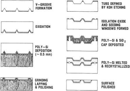
Figure 8-22 Process sequence employed to isolate single-crystal Si tubs. (Left) Conventional dielectric isolation process. (Right) LEGO process.
(Courtesy of G. K. Celler, AT&T Bell Laboratories.)
An alternate process for broad-area lateral epitaxial growth over SiO2 (i.e., Si on SiO2 or SOI) employs a strip heat source in the form of a hot graphite or tungsten wire, scanned laser, or electron beam. After patterning the polycrystalline or amorphous Si on the oxide, the strip sweeps laterally across the wafer surface. Local zones of the surface then successively melt and recrystallize yielding, under ideal conditions, one large epitaxial Si film layer.
Lateral-overgrowth epitaxy is not only limited to silicon technology. An interesting example occurs in the processing of blue GaN lasers. As shown in Fig. 8-23, the buffer layer of GaN deposited on (0001) Al2O3 (sapphire), although smooth, contains too high a dislocation density for the fabrication of reliable devices. However, by utilizing a SiO2 mask containing an array of windows, subsequently deposited GaN films seed or nucleate within them as single crystals. These grow into relatively thick crystalline overgrowths that laterally coalesce to yield a continuous layer. Importantly, a relatively defect-free epitaxial layer is created since the propagation of threading dislocations is effectively curtailed at the constricted seed windows. Diode lasers (Fig. 8-20) fabricated on this top layer have displayed 10,000 h lifetimes during continuous operation at room temperature (Ref. 2).
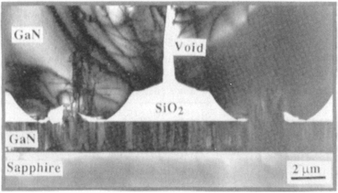
Figure 8-23 Cross-sectional TEM micrograph of laterally overgrown GaN film on a SiO2 mask and window areas.
(From Ref. 2. Reprinted with the permission of the author.)
8.5.3 CVD-BASED EPITAXY
In the CVD-based epitaxial film deposition processes considered now, two gaseous precursors, one for each atomic group, are generally employed, and compound-semiconductor films are produced at pressures ranging anywhere from ∼ 0.5 to 760 torr. Deposition is carried out at temperatures many hundreds of degrees lower than the melting point of the semiconductor. This fact underscores an important distinction that should be noted between prior processes to produce epitaxial films and the ones discussed in subsequent sections. For example, the epitaxy of Si (Section 6.3.2), LPE growth from the melt (Section 8.5.2.1), and even the reversible transport vapor-phase epitaxy (VPE) of GaAs by chloride or hydride CVD processes (Section 6.2.6), are all carried out at elevated temperatures, and thus close to thermodynamic equilibrium. These deposition processes therefore can usually be reversed from film growth to film etching or dissolution through change in temperature. Since the net film-deposition rate is the difference between the rates of adatom–substrate bonding and atomic desorption or reevaporation, near thermodynamic equilibrium the film growth rate is a small difference between large numbers.
In contrast, the processes now considered, particularly MOCVD and later MBE (Section 8.6.2), are conducted at relatively low temperatures and further from thermodynamic equilibrium. Atomic desorption and reevaporation rates are reduced while vapor impingement and adatom– substrate bonding rates remain unchanged, leading to high film-deposition rates. The difference between reversible and a more nearly irreversible film deposition has important ramifications with respect to film-thickness uniformity. In the former case, difficult-to-control high rates of film growth and etching tend to make for rougher films. On the other hand, smoother film surfaces and sharper interfaces between successive deposited layers are a consequence of low-temperature deposition. This is one of the advantages of MOCVD relative to VPE and LPE in the growth of high-performance epitaxial films.
8.5.3.1 Metalorganic CVD Processes for Semiconductor Epitaxy
We have already discussed various MOCVD processes in connection with the deposition of metal and oxide films (Section 6.6.4); whereas the former invariably deposit in polycrystalline form, oxide films assume structures ranging from amorphous to polycrystalline. However, MOCVD was invented to deposit III–V and II–VI compound semiconductor films where it is always the intent to grow high-quality single-crystal or epitaxial films (Refs. 43-45). For this reason the acronyms MOVPE (metalorganic) or OMVPE (organometal) vapor-phase epitaxy are equivalently used when speaking of processes to deposit epitaxial films. In overcoming the shortcomings of the earlier chloride and hydride CVD methods, MOCVD has been particularly effective in preparing films for a variety of visible and long-wavelength lasers as well as quantum-well devices.
8.5.3.1.1 Precursors
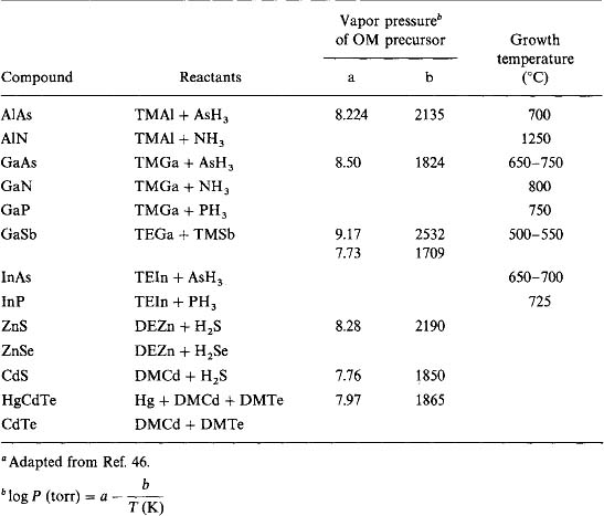
Availability of suitable precursors is critical to the success of MOCVD processes (Ref. 46). Over the years a workable number have been synthesized and some of these are entered in Table 8-3. Among the attributes precursors must possess are adequate volatility, a sufficiently large temperature window between evaporation and decomposition, clean decomposition at relatively low temperatures, good shelf life, manufacturability (yield, cost), and, importantly, low toxicity. Chemically, precursors largely consist of metal alkyl compounds with methyl (M) and ethyl (E) groups present in twofold (di, D) or threefold (tri, T) coordination. Vapor pressures for some precursors are also entered together with typical semiconductor deposition-temperatures.
8.5.3.1.2 Gas Reactions
These metalorganic precursors undergo two main types of CVD reactions. In the first they are reacted with very pure and inexpensive Group V gaseous trihydrides (AsH3, PH3, SbH3), e.g., TMGa and AsH3 to deposit GaAs (Eq. 6-13). However, as hydrides are extremely toxic, safer but more costly Group V alkyl substitutes, e.g., TMAs, TEAs (triethylarsenic), TMP, and TESb, have been developed. This makes possible a second type of reaction, an all-alkyl gas pyrolysis such as
In addition, metalorganic compounds such as DEZn and bicyclodipenta-dienylmagnesium (Cp2Mg) are available for doping purposes. A constant concern with organic gases, however, is incorporation of carbon dopant. Variations in film growth rates are relatively small for alternative MOCVD precursors delivering the same element.
8.5.3.1.3 Reactors
The design of MOCVD reactors means confronting issues frequently absent in other CVD systems. These include the efficient delivery of expensive precursors, the generally hazardous nature of the gases, the often severe temperature gradients in the system, and precise pressure control and valving necessary to deposit multilayer films. The latter capabilities are critical in order to maintain atomically abrupt interfaces in high-performance optoelectronic devices, e.g., quantum-well lasers. To ensure film growth uniformity, substrates usually face upward and lie horizontally on a rotating platform where they are exposed to showerheads or gas nozzles that supply the Group III and V precursors from above as shown in Fig. 8-24. Under such conditions (Refs. 47, 48) the boundary-layer thickness (δ) varies as δ(cm) ∼ [Pω]−1/2;, where P is the reactor pressure and ω is the substrate angular velocity. Certain critical gas-flow parameters are also dependent on ω. For example, the Reynolds number, Re ![]() rd ρω/η, where rd is the substrate disk radius, ρ is the density, and η is the viscosity. In addition, a mixed convection parameter (MCP) has been defined (Ref. 48) as MCP = g{(Td/T∞–1)/(ω3/2η1/2)}, where g is the gravitational constant, and Td and T∞ are the temperatures of disks with radii rd and infinity, respectively. Increasing ω causes Re to rise and MCP to decline. Avoidance of unstable flows, therefore, requires a trade-off between these two dimensionless numbers, e.g., Re < 2000, MCP < 2. It is found that rotational speeds of several hundred to a thousand rpm are optimum in order to reduce δ in a controlled way while avoiding turbulent gas flow. Utilizing computer-controlled gas exchange and supply systems, high-quality, epitaxial multilayer semiconductor structures have been grown in reactors containing a 42-cm diameter rotating disk that accommodates thirty-eight 2.5 cm or nine 10 cm diameter wafers. In addition to GaAs, other III–Vas well as II–VI and IV–VI semiconductor compound films have been synthesized this way.
rd ρω/η, where rd is the substrate disk radius, ρ is the density, and η is the viscosity. In addition, a mixed convection parameter (MCP) has been defined (Ref. 48) as MCP = g{(Td/T∞–1)/(ω3/2η1/2)}, where g is the gravitational constant, and Td and T∞ are the temperatures of disks with radii rd and infinity, respectively. Increasing ω causes Re to rise and MCP to decline. Avoidance of unstable flows, therefore, requires a trade-off between these two dimensionless numbers, e.g., Re < 2000, MCP < 2. It is found that rotational speeds of several hundred to a thousand rpm are optimum in order to reduce δ in a controlled way while avoiding turbulent gas flow. Utilizing computer-controlled gas exchange and supply systems, high-quality, epitaxial multilayer semiconductor structures have been grown in reactors containing a 42-cm diameter rotating disk that accommodates thirty-eight 2.5 cm or nine 10 cm diameter wafers. In addition to GaAs, other III–Vas well as II–VI and IV–VI semiconductor compound films have been synthesized this way.
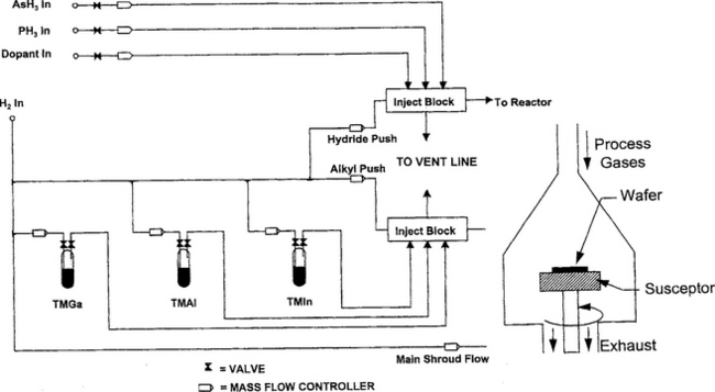
Figure 8-24 Simplified schematic of a III–V MOCVD system showing the gas delivery system and vertical rotating disk reactor.
(From A. G. Thompson, Materials Letters 30, 255 (1997). Reprinted with the permission of the author.)
The deposition of GaN-based films for blue-green-violet photonic devices (Section 8.4.4.3) represents an important triumph for MOCVD methods. Because of the very high equilibrium nitrogen vapor pressures for GaN and InN, growth of InGaN films poses a great challenge. Unusually high nitrogen/Group III (e.g., TMGa) partial pressure ratios of 1000 or more are required, and the nitrogen source gases (N2, NH3) must be efficiently delivered to substrates typically maintained at ∼ 550°C for InN and ∼ 900°C for GaN (Ref. 49). Special reactors with high gas flow capabilities have been built for this purpose.
8.5.3.1.4 Film Growth Rate
Film growth rates (![]() ) and compositions for CVD processes are directly dependent on gas partial pressures (P) and volume flow rates (
) and compositions for CVD processes are directly dependent on gas partial pressures (P) and volume flow rates (![]() ). Let us consider the case of III–V compound semiconductor MOCVD in the mass-transport limited regime. It is assumed there is an abundance of the group V element and that pyrolysis of group III alkyl molecules is complete, yielding monomers. The perfect gas law suggests that the growth rate for a binary compound film is given by (Ref. 50)
). Let us consider the case of III–V compound semiconductor MOCVD in the mass-transport limited regime. It is assumed there is an abundance of the group V element and that pyrolysis of group III alkyl molecules is complete, yielding monomers. The perfect gas law suggests that the growth rate for a binary compound film is given by (Ref. 50)
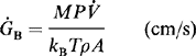 (8-10)
where M and ρ are its molecular weight and density, respectively, A is the area of deposition, and kBT has the usual meaning. In the case of ternary column III sublattice alloys, the growth rate (GT) is given by the sum of two such terms, one for each element, i.e.,
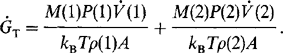 (8-11)
If, for example, we were considering AlxGa1-XAs films, 1 would refer to Al, 2 to Ga, M(1) to AlAs, and M(2) to GaAs. The stoichiometric constant x is simply given by
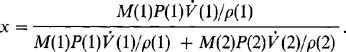 (8-12)
There may be other integer prefactors for the PV terms if any of the alkyl sources is other than a monomer; thus for TMAl, a dimer, all terms involving Al would be multiplied by 2. Also, in the reaction-controlled regime for film growth, equations 8-10 and 8-11 would be multiplied by a temperature-dependent rate constant.
8.5.3.2 Atomic Layer Epitaxy (ALE)
This CVD-based technique enables the growth of epitaxial compound-semiconductor films an atom layer at a time (Refs. 51, 52). For this reason ALE has also been called digital epitaxy. To see how it works let us consider Fig. 8-25, where the binary compound AB is being deposited on an AB substrate surface that is terminated by a layer of A–and B–atoms (–denotes a bond). We assume that the precursors for atoms A and B, molecular AC and BD, respectively, have high vapor pressures. Furthermore, the chemical bonding between A and B is assumed to be stronger than that between A–A and B–B pairs. Upon introducing the AC precursor (1) the reaction with B atoms on the substrate effectively create a surface layer of B– A –together with weakly held C. If the growth temperature is sufficiently high, excess AC merely reevaporates and film growth is self-limiting (2). To add another monolayer the reactor is purged of AC, and BD precursor is introduced (3).
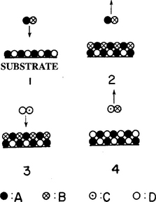
Figure 8-25 Schematic of the atomic layer epitaxy process. The process steps are described in the text.
(From T. F. Kuech, Proc. IEEE 80, 1609, 1992. Reprinted with the permission of the author.)
The B atoms will now combine with the A–atoms to form the B–A–B–structure, and as before, excess BD evaporates. But in addition, C and D react and the CD molecular by-product desorbs leaving an AB film layer behind (4). Through successive cycles of stepwise deposition, films of the desired thickness can be deposited without precise control of process variables.
In the II–VI compounds ZnS, ZnTe, and ZnSe epitaxial film growth by ALE is even simpler than described above; the precursors can simply be the individual atomic species, e.g., Zn and S2. But for the III–V semiconductors, ALE growth is more difficult because the group III elements, e.g., Ga and In, have much lower vapor pressures than corresponding elements from group V. Raising the temperature to promote group III atom volatility results in group V atom loss and film degradation. Therefore, instead of elemental sources, atomic layer epitaxy in III–V semiconductors is accomplished using molecular precursors as in Fig. 8-25, particularly metalorganics for the group III metal (e.g., Ga(CH3)3) and a hydride, e.g., PH3, AsH3, for the group V element. In the case of GaAs growth the first step involves thermal cracking of hydrides which generates AsHx (with x = 1, 2) and As4 products; the As (i.e., A) then directly reacts with the substrate-surface terminated Ga- (i.e., B). Reaction of remaining hydrogen with the metalorganic precursor gas liberates Ga, which bonds to the monolayer of As-, as well as the volatile by-product CH4 (i.e., DC). It is clear that narrow processing temperature windows for condensation, reaction, precursor decomposition, and reevaporation must be optimized. The adsorption–desorption kinetics presented earlier (Section 7.2.5), extended to include surface chemical reactions, can help to model such ALE processes.
In addition to compound semiconductors, other materials have been grown by ALE methods, including elements (e.g., Si, Ge); oxides (e.g., Al2O3, SnO2, In2O3); nitrides (e.g., TiN, TaN); and superconductors (e.g., δ-NbN, YBa2Cu3O7). Employing ALE-grown materials, devices such as monolayer (delta) doped field-effect and heterojunction transistors, as well as quantum-well lasers and superlattice structures, have been demonstrated. Selective epitaxy, side-wall coverage, and monolayer etching are some of the unique features of ALE. On the other hand, low overall film-deposition rates and the complexity of purging and sequencing precursors are decided disadvantages.
8.5.3.3 Additional CVD Epitaxy Processes
In closing, a couple of novel concepts to produce epitaxial films will be briefly addressed. The first, known as vapor-levitation epitaxy, or VLE, is schematically shown in Fig. 8-26. In this process a heated substrate is levitated above a nitrogen track close to a porous frit through which the hot gaseous reactants pass. Upon impingement on the substrate, chemical reactions and film deposition occur while product gases escape into the effluent stream. The gas velocity increases while the gas-concentration profile exhibits depletion as a function of radial distance from the center of the circular substrate. These effects cancel one another and uniform films are deposited. The VLE process was designed for the growth of epitaxial III–V semiconductor films and has certain advantages worth noting:
1. There is no physical contact between substrate and reactor.
2. Thin layer growth is possible.
3. Sharp transitions can be produced between films comprising multilayer stacks.
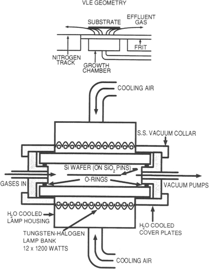
Figure 8-26 (Top) Illustration of VLE process. (Bottom) Schematic of RTCVD process.
(Courtesy of M. L. Green, AT&T Bell Laboratories.)
The second method, known as rapid-thermal CVD processing (RTCVD), enables epitaxial deposition through rapid, controlled variations of substrate temperature. Source gases (e.g., halides, hydrides, metalorganics) react on low thermal-mass substrates heated by radiation from external high-intensity lamps (Fig. 8-26). The latter undergo rapid temperature excursions, and heating rates of hundreds of degrees Celsius per second are possible. In the case of III–V semiconductors, high-quality epitaxial films have been deposited by first desorbing substrate impurities at elevated temperatures followed by immediate lower temperature growth (Ref. 53).
Lattice-matched, atomically sharp heterojunction interfaces can be grown by RTCVD methods, particularly with metalorganic precursors. Only molecular beam epitaxy, considered next, can match or exceed these capabilities.
8.6 LOW-TEMPERATURE METHODS FOR DEPOSITING EPITAXIAL SEMICONDUCTOR FILMS
8.6.1 SCOPE
Descriptors such as low temperature, physical, and high vacuum serve to distinguish some of the epitaxial-film deposition processes treated here from those discussed in the previous section. In addition to the well-known and widely used ultrahigh-vacuum MBE methods, a number of hybrid MBE–CVD processes will be discussed and compared. The intent of these is to usually grow lattice-matched III–V compound-semiconductor films. In contrast, a novel ultrahigh-vacuum, low-temperature CVD process devoted to the epitaxial deposition of Gex Si1–x films will also be described. These strained epitaxial films are now the basis of high-speed electronic devices and have assumed considerable importance. This section ends with a brief discussion of some lesser-known processes for depositing epitaxial films.
8.6.2 MOLECULAR BEAM EPITAXY
This conceptually simple single-crystal film-growth technique represents the state of the art attainable in deposition processes from the vapor phase (Ref. 54). Molecular beam epitaxy essentially involves highly controlled evaporation in an ultrahigh vacuum (˜ 10−10 torr) system. The reaction of one or more evaporated beams of atoms or molecules with the single-crystal substrate yields the desired epitaxial film. High-quality film-growth only ensues if the surfacediffusion-incorporation time (τdi) is less than for the deposition of a monolayer. If these two times are reversed, unincorporated atoms will be physically buried by the incoming monolayer and give rise to defective layers. Since τdi is thermally activated, a low growth temperature limit is implied for good epitaxy. For example, at typical MBE growth rates in the range of 1 μm/h, excellent quality AlGaAs can be grown at temperatures as low as ∼ 680°C, GaAs as low as ∼ 475°C, and InAs as low as ∼ 350°C. In these results it appears that the Group III species governs the growth temperature. Thus, higher temperatures are required for AlxGa1–xAs because AlAs is thermally more stable than GaAs. For InP growth from In and P2 beams on (100) InP, substrate temperatures of 350–380°C have been used. Similarly, InxGa1–xAs films, lattice matched to InP, have been grown between 400 and 430°C. Recommended substrate temperatures for MBE growth of GaAs range from 500 to 630°C and are higher than the minimum ones quoted. The MBE deposition window (Section 3.2.3.2), film structure, and morphology have been comprehensively and authoritatively treated by Tsao (Ref. 55) in terms of fundamental thermodynamic, kinetic, and defect issues.
A modern MBE system is displayed in the photograph of Fig. 8-27. It features independent control of beam sources and film deposition, cleanliness, and real-time structural and chemical characterization capability. In such systems precise fabrication of semiconductor heterostructures from a fraction of a micron thick down to a single monolayer is possible. The heart of an MBE deposition system is shown schematically in Fig. 8-28a. Arrayed around the substrate are semiconductor and dopant atom heating sources consisting of either effusion cells or electron-beam guns. The latter are employed for the high-melting Si and Ge materials. On the other hand, effusion cells are used to evaporate compound-semiconductor elements and their dopants. An effusion cell is essentially an isothermal cavity containing a hole through which the evaporant exits; it behaves like a small-area source and exhibits cosφ vapor emission. Vapor pressures of important compound semiconductor species are displayed in Fig. 3-2.
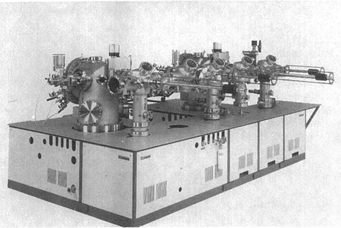
Figure 8-27 Photograph of multichamber MBE system.
(Courtesy of Riber Division, Inc. Instruments SA.)
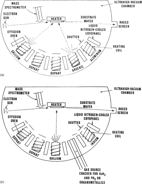
Figure 8-28 Arrangement of sources and substrate in (a) conventional MBE system; (b) MOMBE system.
(Courtesy of M. B. Panish, AT&T Bell Laboratories.)
Consider now a substrate positioned a distance L from a source aperture of area A, with φ = 0. An expression for the number of evaporant species striking the substrate is
As an example consider a Ga source in a system where A = 5 cm2 and L = 12 cm. At T = 900°C the vapor pressure PGa ![]() 4.2 × 10⁻⁴ torr and substituting MGa = 70, the arrival rate of Ga at the substrate is calculated to be 5.69 × 10¹⁴ atoms/cm2-s. The As arrival rate is usually much higher and, therefore, film deposition is controlled by the Ga flux. An average monolayer of GaAs is 2.83 Å thick and contains 6.3 × 10¹⁴ Ga atoms/cm2. Hence, the growth rate is calculated to be (5.69 × 1014 × 2.83 × 60)/6.3 × 1014 = 153 Å/min, a value typically an order of magnitude lower than for CVD growth rates.
4.2 × 10⁻⁴ torr and substituting MGa = 70, the arrival rate of Ga at the substrate is calculated to be 5.69 × 10¹⁴ atoms/cm2-s. The As arrival rate is usually much higher and, therefore, film deposition is controlled by the Ga flux. An average monolayer of GaAs is 2.83 Å thick and contains 6.3 × 10¹⁴ Ga atoms/cm2. Hence, the growth rate is calculated to be (5.69 × 1014 × 2.83 × 60)/6.3 × 1014 = 153 Å/min, a value typically an order of magnitude lower than for CVD growth rates.
In many applications GaAs/AlxGa1–xAs multilayers are required. For this purpose the Ga and As beams are on continuously while the Al source is operated intermittently. Actual growth rates are determined by the measured layer thickness divided by the deposition time. The fraction × can be determined from the relation
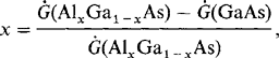 (8-14)
where the respective growth rates (![]() ) must be known.
) must be known.
8.6.2.1 Gas Source MBE
Although MBE, which uses solid sources for both group III and V elements, has been extremely successful for the growth of arsenides and antimonides, it has been less useful for phosphides (Ref. 54). The very high vapor pressure of phosphorus has meant excessive desorption relative to incorporation in growing films. To offset this desorption, the V/III flux ratio is an order of magnitude higher than for arsenides. The large quantities of P employed means physically big sources which stretch the capacity of pumping systems. It was primarily as a response to difficulties with phosphorus that gas-source MBE was introduced into compound semiconductor technology (Ref. 56). Because the process shown in Fig. 8-28b incorporates a gas source to supply group V elements, terms such as gas-source molecular beam epitaxy (GSMBE) or, less commonly, chemical beam epitaxy (CBE) have been coined. Organometallics, often used for this purpose, are thermally cracked, releasing the group V element as a molecular beam into the system. Hydride gas sources, e.g., AsH3, PH3, have also been similarly employed for this purpose. Excellent epitaxial-film quality has been obtained in these hybrid MBE–MOVPE processes. A final process known by the acronym MOMBE employs metalorganics for the group V elements and solid group III elements.
MBE systems have been employed in manufacturing environments since 1984 to fabricate GaAs laser diodes (Ref. 57) and since 1986 to make monolithic microwave integrated circuits and high-power heterojunction bipolar transistors (Ref. 58). Surface defect densities less than 10 cm− 2 have been attained by optimizing the function of the group III Knudsen cell. More recently, GSMBE systems using an AsH cracker source have been built to continuously deposit 1.7 thick metal–semiconductor field-effect transistor (MESFET) structures with growth occurring at 540°C and 10−5 torr. Multiwafer throughput of four 10 cm diameter or seven 3 cm diameter wafers per 2.5 h, using a vacuum load-locked capability of recharging 500 cm3 Knudsen cells of Ga, Al, and In, gives an idea of the operation scale. Electrical (sheet) resistance variations of less than 2% (over a 27 cm diameter area), GaAs electron mobilities as high as 124,000 cm2/V-s (77 K), and an oval defect density of ∼ 40 cm−2 are indicative of the excellent quality of the epitaxy.
8.6.2.2 MBE vs OMVPE: Advantages and Disadvantages
These two epitaxy techniques have emerged as the ones of choice in high-performance applications (Ref. 54). Relative to LPE and VPE they both readily enable near-atomic film/substrate interface abruptness, high levels of doping uniformity, and growth of multilayered structures having different compositions and doping levels. When compared to OMVPE, MBE’s former advantage in interface abruptness no longer exists. However, MBE growth is further removed from thermodynamic equilibrium so that films are produced at lower substrate temperatures. Perhaps the greatest advantage of MBE is the vacuum environment that makes possible the in situ diagnostic capabilities of reflection high-energy electron diffraction (RHEED) and mass spectrometry. Discussed later in Section 8.7.4.2, the former technique yields precise monolayer growth rates and provides a measure of film smoothness; the latter is used to monitor desorption of species from chamber wall or depositing film surfaces. Relative safety is another advantage of MBE as the metalorganic sources are often toxic and or pyrophoric. Advantages of OMVPE include two to three times greater film growth rates, less maintenance downtime, and little difficulty in depositing phosphorus. Although the situation has occasionally flip-flopped, transistor and laser diode device characteristics from MBE-grown III–V materials have generally exceeded those of devices prepared by OMVPE.
8.6.3 SILICON HETEROEPITAXY
Since the early 1960s Si has been the semiconductor of choice. Its dominance cannot, however, be attributed solely to its electronic properties, for it has mediocre carrier mobilities and only average breakdown voltage and carrier saturation velocities. The absence of a direct bandgap rules out light emission and severely limits its efficiency as a photodetector. Silicon does, however, possess excellent mechanical and chemical properties. A high modulus of elasticity and high hardness enable Si wafers to withstand the rigors of handling. Its great natural abundance, ability to be readily purified, possession of a highly inert and passivating oxide, and ease of device processing have all helped to secure a dominant role for Si in solid-state technology. Nevertheless, Si is being increasingly supplanted in high-speed applications by compound semiconductors.
The idea of combining semiconductors which can be epitaxially grown on low-cost Si wafers is very attractive. Monolithic integration of III–V devices with Si integrated circuits offers the advantages of combined photonic–electronic functionality and higher speed signal processing distributed over larger substrate areas. Furthermore, Si wafers are more robust and dissipate heat more readily than GaAs wafers. Unfortunately, there are severe crystallographic as well as chemical compatibility problems that limit Si-based heteroepitaxy. Reference to Table 8-1 reveals that Si is only closely lattice matched to GaP and ZnS. Furthermore, its small lattice constant precludes conventional epitaxial matching to III–V semiconductor alloys.
8.6.3.1 Wafer Bonding
Direct wafer bonding refers to the phenomenon of making mirror-polished, flat and clean wafers of almost any materials adhere to each other by bringing their surfaces into contact; van der Waals forces are the source of the bonding. Special treatments are required to make the surfaces hydrophilic (with one or two monolayers of oxygen or water) or hydrophobic (hydrogen-covered due to a HF dip); such surfaces facilitate subsequent bonding, e.g., by hydrogen bridge bonds. Assorted combinations such as Si–Si, Si–SiO2–Si for silicon-on-insulator (SOI) technology (Section 8.5.2.2), and Si-based heteroepitaxial structures with large substrate mismatches have been fabricated by these methods (Ref. 59).
In wafer bonding the epi-film layer (X) is first deposited on a lattice-matched substrate (Y). Then a clean, atomically flat Si wafer is bonded, usually with applied heat and pressure, to the similarly flat Y–X–combination so as to produce a Y–X–Si sandwich. After substrate Y is chemically etched off, the desired X–Si pair remains. By these means wafer-bonded, III–V semiconductor/Si heteroepitaxial structures of large lattice mismatch have been fabricated containing misfit dislocations but apparently no threading dislocations.
Despite the exciting possibilities of wafer bonding, GexSi1–x/Si strained-layer epitaxy appears to be the primary basis for future silicon heterostructures.
8.6.3.2 Ultrahigh-Vacuum Chemical-Vapor Deposition (UHV/CVD)
This relatively new process pioneered by Meyerson (Refs. 60, 61) challenges our conventional notions regarding CVD processes, particularly the high-temperature epitaxial deposition of silicon. As noted in Section 6.3.2, Si epitaxy is normally practiced well above 1000°C in atmospheric or sometimes in low-pressure (10–100 torr) reactors. Desorption of water vapor and oxygen contaminants as well as native oxide from the silicon surface, so necessary for high-quality epitaxy, is a result of the high temperatures employed. But, such temperatures also cause troublesome redistribution of dopants between the substrate and epitaxial layer being grown (autodoping). The evolution of silicon technology to ever-smaller dimensions coupled with heavily doped patterned substrates has made it imperative to limit diffusion by reducing the so-called thermal budget, e.g., 1000°C for 30 min, for epitaxy. Rather than high-temperature surface cleaning a novel approach was to passivate the Si surface ex situ by etching in HF. This simple step produces a monolayer of hydrogen that passivates the Si surface and reduces its tendency to react with H2O and O2 by some 13 orders of magnitude (Ref. 60)! As a result, native oxide does not form; instead the passivated surface can now be exposed to SiH4, which displaces the adsorbed hydrogen and directly reacts with the substrate to produce epitaxial Si. By this strategy an atomically clean Si surface can be obtained at deposition temperatures of ∼ 500°C. To maintain surface cleanliness, the UHV/CVD reactor is typically first pumped to the 10−9 torr range while film growth is carried out at a pressure of ∼ 10−3 torr or lower. In addition to silane, simultaneous gas flows of GeH4, B2H6, and PH3 are used, the first to produce GexSi1–x films and the latter two to dope them. With respect to the latter, excellent control of boron content in Si is achieved through variation of the diborane flow. In addition to GexSi1–x/Si superlattices shown in Fig. 8-29, similar defect-free, highly doped, metastable 10 at.% B–Si/Si multilayer structures have been grown.
Figure 8-29 (a) Cross-sectional TEM image of Gea4Sia6-Si strained-layer superlattice. (b) High-resolution lattice image.
(Courtesy of J. C. Bean and R. Hull, AT&T Bell Laboratories.)
The major application for SiGe technology is the base region of heterojunction bipolar transistors (HBTs). In this device the highly doped GexSi1–x base is pseudomorphically grown over an n-doped Si collector and then covered with a polysilicon emitter. A typical configuration merges these HBTs with their high-frequency capability and Si CMOS for digital applications. Other potential applications for SiGe ranging from wireless communications to optoelectronics including traditional (CMOS) and quantum (resonant tunneling diode) devices have been discussed in the literature (Refs. 61, 62). It now appears that high-speed devices based on SiGe are competitive with those derived from III–V compound semiconductors. The often quoted observation that "GaAs is the material of the future… and it always will be" may have added significance now that SiGe has boosted the performance of Si devices.
8.6.4 LESS COMMON EPITAXY PROCESSES
Just as there are different manifestations of epitaxy, a variety of approaches have been undertaken to produce epitaxial structures and architectures. In this section, several of these unusual techniques are described. In general they are limited to selected materials but include some interesting and potentially important applications.
8.6.4.1 Molecular Beam Allotaxy (MBA)
In this method a buried heteroepitaxial layer is formed upon annealing a subsurface precipitate layer. The MBA process (Ref. 63) can be understood by considering the formation of an epitaxial Si/CoSi2/(100)Si structure. Because of the small lattice mismatch between CoSi2 and Si noted earlier (Section 8.2.3.2), this is a model MBA system. To produce the trilayer epitaxial structure a buffer homoepitaxial Si film is first deposited on a Si wafer within an MBE system at 500– 700°C. Then as the Si flux is maintained constant, Co metal is coevaporated first at a steadily increasing rate, then at a constant rate for some time, and finally at a rate that ramps down to zero. A Si top layer completes the structure. In effect a trapezoidal depth profile of Co in the form of small-to-large-to-small CoSi2 precipitates buried within the Si matrix results. When these precipitates are annealed to temperatures of 1100–1200°C they coalesce into CoSi2 layers with flat and atomically abrupt interfaces. The growth mechanisms, i.e., Ostwald ripening and sintering, already discussed (Section 7.4.5) are responsible for the enlargement of the bigger precipitates at the expense of the smaller ones. A similar continuous buried β-FeSi2 layer has been prepared by MBA. However, the Si cap layer contained many twins and is considerably more defective than is the case for CoSi2.
8.6.4.2 Mesotaxy
The same objective, buried disilicide layers embedded in silicon, can also be realized by an ion-implantation process known as mesotaxy. In the case of CoSi2 200 keV Co + ions are implanted into Si at fluences of ∼ 2 × 10¹⁷ ions/cm2 resulting in a Gaussian distribution of metal atoms. This is followed by annealing treatments at 1000°C during which time the Co concentration profile narrows by similar coalescence phenomena while the surrounding lattice damage is significantly reduced. Abrupt epitaxial silicide layers buried 1000Å beneath the Si surface have been produced this way (Ref. 64).
Through similar ion implantation of oxygen ions into silicon at high energies and fluences, followed by annealing, highly insulating, subsurface layers of amorphous SiO2 films have been produced. Ion-beam synthesis of buried SiO2 is known as SIMOX (separation by implanted oxygen). Together with MBA and mesotaxy they represent important potential processes for the eventual realization of three-dimensional integrated circuits.
8.6.4.3 van der Waals Epitaxy
We have already noted the severe restriction on heteroepitaxy imposed by lattice mismatch between materials containing strong ionic or covalent bonds. However, one might imagine conditions for epitaxy to be relaxed on substrate surfaces that do not contain the dangling electrons which promote chemical bonding across interfaces. In the absence of the latter we speak of an epitaxy based on weak van der Waals interactions (Ref. 65). Suitable surfaces for such purposes stem from easily cleaved materials, or semiconductors whose bonds are terminated by specific atoms, e.g., S or Se on (111) GaAs, H on Si(111), and F on CaF2. Among the inorganic film/substrate van der Waals epitaxy systems that have been studied are Se/Te; TMX2/SnS2; TMX2/mica; TMX2/S–GaAs(111); GaSe/Se–GaAs(111); and GaSe/H–Si(111), where TM is a transition metal, e.g., Mo, Nb, and X is S, Te, or Se. Epitaxial organic films, e.g., phthalocyanines/TMX2 and C60/TMX2, have also been prepared. In virtually all cases large lattice mismatches are involved, but good epitaxial growth has been claimed.
8.6.4.4 Colloidal Epitaxy
The concept of epitaxy has extended beyond merely arranging atoms on a crystalline substrate, to depositing colloidal particles on a geometrically patterned substrate template. In this way, colloidal silica particles with a 0.525 μm radius have been made to controllably settle onto a substrate lithographically patterned with an FCC (100) planar array of accommodating holes (Ref. 66). The result is a periodic three-dimensional, microporous dielectric structure known as a photonic crystal. These crystals have unique optical properties and are claimed to "manipulate light the way superconductors manipulate electrons" (Ref. 67).
8.7 MECHANISMS AND CHARACTERIZATION OF EPITAXIAL FILM GROWTH
In this section we explore the interactions of depositing atoms with surfaces leading to the incorporation of atoms into growing epitaxial films. Mechanisms involving molecular beams have been most studied because characterization instrumentation is usually more readily incorporated into MBE chambers than CVD systems. For this reason there will be some discussion of MBE-based diffraction methods that have revealed so much about the structure of surfaces as well as films that grow on them. Finally the important subject of selective epitaxy will also be addressed to close the chapter.
8.7.1 HOMOEPITAXY OF SILICON
One may expect that the kinetics of MOMBE film growth (Ref. 68) of Si would parallel that of thermal CVD Si homoepitaxy treated in Section 6.3.2. For example, the deposition of epitaxial silicon on Si(001) employing a Si2H6 precursor yielded an Arrhenius curve of growth rate vs temperature quite similar to that of Fig. 6-13. However, in MOMBE a transition from reaction control to flux (gas transport) control occurred at about 600°C compared to 1000°C in CVD. Below this temperature the rate of silicon formation was limited by desorption of reaction product hydrogen in a process occurring with an activation energy of 2.0 eV. Above this temperature desorption is very rapid and film growth is limited only by the precursor flux.
In the case of UHV/CVD deposition of Si, the critical hydrogen adlayer begins to desorb above 400°C with an activation energy of 2.58 eV. Film growth must commence before appreciable surface hydrogen loss occurs. Interestingly, however, SiH4 itself forms an ordered self-terminating adlayer on Si, or an effective epitaxial monolayer at room temperature. The presence of Ge on the Si surface accelerates epitaxial film growth by lowering the activation energy for desorption of the hydrogen by-product.
8.7.2 FILM GROWTH OF GaAs AND RELATED FILMS
8.7.2.1 Kinetics of Adsorption and Desorption
Since the first step in MBE film growth involves surface adsorption, let us first consider a beam of Ga atoms incident on a GaAs surface. Below about 480°C Ga atoms readily physisorb on the surface but above this temperature Ga both adsorbs and desorbs. Time-resolved mass-spectroscopy measurements of the magnitude of the atomic flux desorbing from the substrate have revealed details of GaAs film-growth mechanisms (Ref. 69). The instantaneous Ga surface concentration, nGa, is increased by the incident Ga beam flux, ![]() (Ga), and simultaneously reduced by a first-order kinetics desorption process. Therefore,
(Ga), and simultaneously reduced by a first-order kinetics desorption process. Therefore,
where τ(Ga) is the Ga adatom lifetime and nGa/τ(Ga) represents the Ga desorption flux, •des(Ga). Integrating Eq. 8-15 yields
For a rectangular pulse of incident Ga atoms the detected desorption flux closely follows the dependence of Eq. 8-16. Similarly, when the Ga beam is abruptly shut off, the desorption rate decays as exp – (t/τ(Ga)). The exponential rise and decay of the signal is shown schematically in Fig. 8-30a.
Figure 8-30 Deposition and desorption pulse shapes on (111) GaAs for (a) Ga, (b) As2, (c) As2 on a Ga-covered surface.
(After Ref. 69.)
In the case of As2 molecules incident on a GaAs surface, the lifetime is extremely short so that the desorption pulse profile essentially mirrors that for deposition (Fig. 8-30b), i.e., ![]() des(As2) =
des(As2) = ![]() (As2). However, on a Ga-covered GaAs surface, τ(As2) becomes appreciable with desorption increasing only as the available Ga is consumed (Fig. 8-30c). These observations indicate that in order to adsorb As2 on GaAs, Ga adatoms are essential.
(As2). However, on a Ga-covered GaAs surface, τ(As2) becomes appreciable with desorption increasing only as the available Ga is consumed (Fig. 8-30c). These observations indicate that in order to adsorb As2 on GaAs, Ga adatoms are essential.
8.7.2.2 Mechanisms
Detailed models for epitaxial growth on (100) GaAs with both As2 and As4 precursors have been reviewed more recently by Joyce (Ref. 70). In the case of incident Ga plus As2 fluxes on a Ga-stabilized GaAs surface (defined later), the As2 molecules are first adsorbed into a mobile, weakly bound precursor state that has a residence time of ∼ 10−5 s. First-order dissociative chemisorption on Ga atoms enables As incorporation into the growing film. If the Ga flux is less than half the As2 flux, one As atom sticks to each Ga atom. At low substrate temperatures, association of As2 produces As4 molecules which then slowly desorb. Similarly, when films are grown employing an As4 flux, these molecules are also first adsorbed as a mobile, weakly bound precursor state. This entity migrates along the surface with a diffusive activation energy of 0.25 eV, while its residence time is temperature dependent with a desorption activation energy of 0.4 eV. The sticking coefficient of As never exceeds 0.5, even with a completely covered Ga surface or when the Ga flux exceeds the As4 flux. This fact is explained by assuming a pairwise dissociation of the As4 molecules chemisorbed on adjacent Ga atoms in a second-order reaction. During GaAs growth it is suggested that when two As4 molecules react, four As atoms are incorporated while the other four desorb as As4. For either As precursor under conventional deposition conditions the film growth-rate determining step is the migration rate of Ga adatoms to appropriate lattice sites where reaction occurs. In summary these adsorption/desorption effects strongly underscore the kinetic rather than thermodynamic nature and control of MBE growth.
8.7.2.3 Stabilized and Reconstructed Surfaces
Normally, III–V compound-semiconductor films are grown with a two- to tenfold excess of the group V element. This maintains the elemental V/III impingement flux ratio > 1. For GaAs and AlxGa1–x As, this condition results in stable stoichiometric film growth for long deposition times. In contrast to the preceding so-called As-stabilized growth, there is Ga-stabilized growth which occurs when the flux ratio is approximately 1. An excess of Ga atoms is generally avoided, however, because they tend to cluster into molten droplets.
The (100) and (111) surfaces of GaAs and related compounds exhibit a variety of reconstructed surface geometries dependent on growth conditions and subsequent treatments (Ref. 55). For As- and Ga-stabilized growth, (2 × 4) and (4 × 2) reconstructions, respectively, have been observed on (100) GaAs. Other structures, i.e., C(2 × 8) As and C(8 × 2) Ga, have also been reported for the indicated stabilized structures. To complicate matters further, intermediate structures, e.g., (3 × 1), (4 × 6), and (3 × 6), as well as mixtures also exist within narrow ranges of growth conditions. The complex issues surrounding the existence and behavior of these surface reconstructions are continuing subjects of research.
8.7.2.4 Mechanism of Growth in GaInAsP
During epitaxial film deposition of multicomponent semiconductors the mechanisms of substrate chemical reactions and atomic incorporation can be quite complex. For example, a proposed model of sequential deposition of the first two monolayers of GaInAsP on an InP substrate is depicted in Fig. 8-31 for the hydride process (Ref. 71). The first step is suggested to involve adsorption of P and As atoms. Then GaCl and InCl gas molecules also adsorb in such a way that the Cl atoms dangle outward from the surface. Next, gaseous atomic hydrogen adsorbs and reacts with the Cl atoms forming HCl molecules, which then desorb. Now the process repeats with P and As desorption and when the cycle is completed, another bilayer of quaternary alloy film deposits. This picture accounts for single-crystal film growth and the development of variable As/P and Ga/In stoichiometries.
Figure 8-31 Atomic mechanisms involved in the sequential deposition of GaInAsP on InP.
(Reprinted with permission from J. Wiley & Sons. From Ref. 71.)
8.7.3 SELECTIVE EPITAXY
Compared to actual and potential applications for selective deposition of metal films (Section 6.8.6), selective epitaxial growth (SEG) (also known as selective area epitaxy (SAE), or selected area growth (SAG) of semiconductors promises to have a far greater impact (Ref. 50). By selective epitaxy we mean the growth of single-crystal films over a desired patterned area and nowhere else. The technique has been practiced in both elemental and compound semiconductor materials. Strategies for SEG differ depending on the type of semiconductor and nature of film deposition, i.e., physical or chemical. Most often, selective epitaxy is associated with differential film deposition in windows, opened in masks, relative to the mask itself. In addition, it is required that selective epitaxial films have the same electrical and optical properties as similarly deposited blanket or broad-area films. Surfaces for SEG are not always planar. If, for example, the substrate is textured with a triangular topography, localized epitaxial growth may be concentrated at the V-shaped bottoms as adsorbed species migrate from the peaks, down the slopes, and into the valleys. In such cases crystallography is important in defining the growth morphologies.
8.7.3.1 Selective Epitaxy in Silicon Materials
There is a history of SEG in Si dating back to the early 1960s (Ref. 72). This effort has almost entirely been devoted to fostering nucleation and growth of epitaxial Si on Si surfaces and suppressing these processes on adjoining SiO2 or silicon nitride mask surfaces. It is usually accomplished by CVD processes involving H2 reduction of a chlorosilane, e.g., SiCl4, Si2 Cl2 H2, to deposit Si, and with simultaneous HCl additions to etch away spurious Si nuclei before they coalesce and grow. In an LPCVD-based SEG study using a Si2Cl2H2/HCl/H2 mixture, as many as 105 hemispherical, 0.5 sized cap-shaped Si nuclei per cm2 deposited on dielectric rather than Si surfaces (Ref. 73). Elimination of such an intolerable defect density is critical before any of the applications suggested for selective epitaxy, e.g., filling deep trenches and contact holes, formation of emitter windows in bipolar transistors, processing of DRAM cells and three-dimensional integrated circuits, can be realized. More recently (Ref. 74) selective heteroepitaxial deposition of SiGe films has been studied and the effects of SiO2/Si area ratio, HCl flow rates, temperature, and doping on film growth explored. In contrast to Si the growth of SiGe at low temperatures is strongly dependent on oxide coverage.
8.7.3.2 Selective Epitaxy in Compound Semiconductors
In general, compound semiconductor devices require fewer processing steps than their silicon-based counterparts. A great advantage of selective deposition is the further reduction in the number of steps. In fact, the fabrication of a semiconductor laser wholly by selective epitaxy processing has already been demonstrated (Ref. 75).
In the remainder of this section only III–V semiconductors used for photonic devices will be considered and selective MBE, MOCVD, and MOMBE techniques for their deposition briefly reviewed.
8.7.3.2.1 MBE
Through the imposition of a shadow mask between the molecular beam source and substrate, patterned epitaxial features have been readily produced in GaAs, AlGaAs, and InAs materials. However, the growth of complicated structures necessitates manipulating numerous shadow masks. Furthermore, mask contact with the substrate generates defects, and for these reasons SEG by this method is not feasible. By using deposited SiO2 masks, the latter shortcoming is eliminated. Although high-quality epitaxial films grow in the mask window, a polycrystalline deposit often coats the mask (pseudoselective epitaxy); in addition, the single and polycrystalline regions at the mask edge are generally defective. A key to preventing GaAs nucleation on SiO2 masks is to enhance desorption of Ga adatoms. Elevated growth temperatures and a reduced As flux tend to enhance selectivity. In general, less deposition on the mask and hence greater selectively occurs with GaAs relative to AlGaAs because SiO2 reacts more with Al than with Ga.
8.7.3.2.2 MOCVD
Although selective epitaxy by MBE means is limited by physical variables, MOCVD takes advantage of the greater number of possibilities inherent in varying system chemistry. For example, by using a metalorganic chloride source of Ga, i.e, Ga(C2H5)2Cl instead of, say, (CH3)3 Ga (TMG), selective growth of GaAs over SiO2, si3N4, and SiONx is more readilyachieved (Ref. 76). Apparently GaCl does not adsorb on the mask material, nor is this chloride dissociated to free Ga for deposition. This suggests that Al and In halides may also promote selective growth of AlGaAs and InGaAs. In a similar vein the reaction of AsCl3 together with (CH3)3 Ga inhibited deposition of GaAs onW and Si3N4 masks (Ref. 77). Furthermore, HCl adsorption on the mask may aid etching of any deposit there.
8.7.3.2.3 MOMBE
Although the chemical precursors are the same as for MOCVD, high-vacuum operation eliminates boundary-layer transport and suppresses gas-phase reactions, both of which are conducive to high selectivity. Fewer gas-phase collisions of precursor molecules mean less decomposition and reduced impingement on and interaction with the mask. As a result, greater selectivity is found in MOMBE than in atmospheric MOCVD. A study of selective GaAs deposition employing mass spectroscopy is particularly revealing (Ref. 78). At about 350°C TMG molecules were observed to adsorb, immediately decompose, and release Ga atoms on the GaAs surface. But, on the SiO2 mask surface molecular decomposition did not occur below 535°C. This suggests a processing window for selective epitaxy in this system based on temperature.
8.7.4 IN SITU FILM CHARACTERIZATION OF MBE FILMS
This section deals with two techniques that are capable of monitoring the structure and composition of epitaxial films during in situ growth. Low-energy electron diffraction (LEED) and reflection high-energy electron diffraction (RHEED), which are distinguished in Fig. 8-32, have provided much of our knowledge of epitaxial film growth mechanisms. An ultrahigh-vacuum environment is a necessity for both methods because of the sensitivity of diffraction to adsorbed impurities and the need to eliminate electron-beam scattering by gas molecules. This is why they are limited to use in MBE systems.
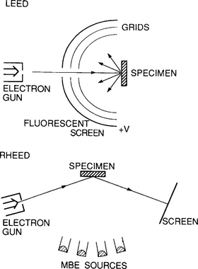
8.7.4.1 LEED
In LEED a low-energy electron beam (10–1000 eV) impinges normally on the film surface and only penetrates a few angstroms below the surface. Bragg’s law for both lattice periodicities in the surface plane results in cones of diffracted electrons emanating along forward and backscattered directions. Simultaneous satisfaction of the diffraction conditions means that constructive interference occurs where the cones intersect along a set of lines or beams radiating from the surface. These backscattered beams are intercepted by a set of grids raised to different electric potentials. The first grids encountered retard the penetration of low-energy inelastic electrons. Diffracted (elastic) electrons of higher energy pass through and, accelerated by later grids, produce illuminated spots on the hemispherical fluorescent screen.
Both LEED and RHEED patterns of the (7 × 7) structure of the Si (111) surface are shown in Fig. 8-33. To obtain some feel for the nature of these diffraction patterns it is useful once again to think in terms of the reciprocal space. Arrays of reciprocal latice points form rods or columns of reciprocal-lattice planes shown as vertical lines pointing normal to the real surface.
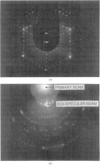
Figure 8-33 (a) LEED pattern of Si surface (38 eV electron energy, normal incidence). (b) RHEED pattern of Si surface (5 keV electron energy, along <112> azimuth).
(Courtesy of H. Gossmann, AT&T Bell Laboratories.)
They are indexed as (10), (20), etc., in Fig. 8-34. Consider now an electron wave of magnitude 2π/λ, propagating in the direction of the incident radiation and terminating at the origin of the reciprocal lattice. Following Ewald we draw a sphere of radius 2π/λ, about the center. A property of this construction is that the only possible directions of the diffracted rays are those which intersect the reflecting sphere at reciprocal lattice points as shown. To prove this we note that the normal to the reflecting plane is the vector connecting the ends of the incident and diffracted rays. But this vector is also a reciprocal lattice vector. Its magnitude is 2π/α, where a is the interplanar spacing for the diffracting plane in question. It is obvious from the geometry that
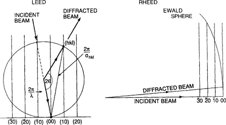
Figure 8-34 Ewald sphere construction for LEED and RHEED methods. The film plane is horizontal, and reciprocal planes are vertical lines.
which reduces to Bragg’s law, the requisite condition for diffraction. When the electron energies are small as in LEED, the wavelength is relatively large, yielding a small Ewald sphere. A sharp spot diffraction pattern is the result. The intense hexagonal spot array of Fig. 8-33a reflects the sixfold symmetry of the (111) plane while the six fainter spots in between are the result of the (7 × 7) surface reconstruction.
8.7.4.2 RHEED
An immediate advantage of RHEED is that the measurement apparatus does not physically interfere with deposition sources in an MBE system the way LEED does. This is one reason why RHEED has become the overwhelmingly preferred real-time film characterization accessory in MBE systems. In RHEED the electron beam is incident on the film surface at a grazing angle of a few degrees at most. Electron energies are much higher than for LEED and range from 5 to 100 keV. From the standpoint of diffraction, the high electron energies lead to a very large Ewald sphere (Fig. 8-34). The reciprocal lattice rods have finite width due to lattice imperfections and thermal vibrations; likewise, the Ewald sphere is of finite width because of the incident electron-energy spread. Therefore, the intersection of the Ewald sphere and rods occurs for some distance along their height, resulting in a streaked rather than spotty diffraction pattern. During MBE film growth both spotted and streaked patterns can be observed; spots occur as a result of three-dimensional volume diffraction at islands or surface asperities while streaks characterize smooth layered film growth. These features can be seen in the RHEED patterns obtained from MBE-grown GaAs films (Fig. 8-35).
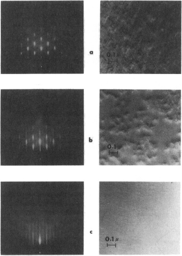
Figure 8-35 RHEED patterns [40 keV, (110) azimuth] and corresponding electron micrograph replicas (38,400 ×) of same GaAs surface. (a) Polished and etched GaAs substrate heated in vacuum to 580°C for 5 min. (b) 150 Å film of GaAs deposited; (c) 1 of GaAs deposited.
(From Ref. 69. Courtesy of A. Y. Cho, AT&T Bell Laboratories.)
8.7.4.3 RHEED Oscillations
An important attribute of the RHEED technique is that the diffracted beam intensity is relatively immune to thermal attenuation arising from lattice vibrations. This makes it possible to observe the so-called RHEED oscillations during MBE growth of epitaxial semiconductor films. In the case of GaAs the intensity of the specular RHEED beam undergoes variations which track the step density of Ga on the growing surface layer. If we consider Fig. 8-36 and associate the maximum beam intensity with the flat surface where the fractional coverage ![]() = 0 (or
= 0 (or ![]() = 1), then the minimum intensity corresponds to
= 1), then the minimum intensity corresponds to ![]() = 0.5. During deposition of a complete monolayer, the beam intensity, initially at the crest, falls to a trough and then crests again. Film growth is, therefore, characterized by an attenuated, sinelike wave with a period equal to the monolayer formation time. Under optimal conditions the oscillations persist for many layers and serve to conveniently monitor film growth with atomic resolution. The temperature above which RHEED oscillations are expected can be easily estimated. To allow a few atomic jumps to occur in order to smooth terraces before they are covered by a monolayer (per second) requires a diffusivity of roughly 10−15 cm2/s. By the example given in Section 7.4.3, RHEED oscillations are predicted to occur above 0.2TM, 0.12TM, and 0.03TM on group IV element, metal, and alkali halide substrates, respectively, in rough qualitative agreement with experiment.
= 0.5. During deposition of a complete monolayer, the beam intensity, initially at the crest, falls to a trough and then crests again. Film growth is, therefore, characterized by an attenuated, sinelike wave with a period equal to the monolayer formation time. Under optimal conditions the oscillations persist for many layers and serve to conveniently monitor film growth with atomic resolution. The temperature above which RHEED oscillations are expected can be easily estimated. To allow a few atomic jumps to occur in order to smooth terraces before they are covered by a monolayer (per second) requires a diffusivity of roughly 10−15 cm2/s. By the example given in Section 7.4.3, RHEED oscillations are predicted to occur above 0.2TM, 0.12TM, and 0.03TM on group IV element, metal, and alkali halide substrates, respectively, in rough qualitative agreement with experiment.
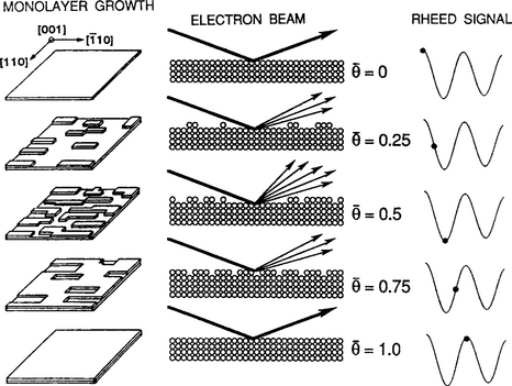
Figure 8-36 Real space representation of the formation of a single complete monolayer. θ is the fractional layer coverage. Corresponding RHEED oscillation signal is shown.
What we have said strictly applies to MBE growth on unstepped or singular planes. But what about growth on vicinal surfaces roughened by steps and terraces of length h? At low temperatures, the surface-diffusion length of adatoms is less than h and two-dimensional nucleation of monolayer islands occurs as on a singular plane. These are the conditions that lead to RHEED oscillations. However, at elevated temperatures the adatom migration length exceeds h and step edges now become a favored sink for adatoms (Ref. 70). Instead of island formation and coalescence with a progressive buildup of ![]() , film growth now proceeds by step propagation across a featureless terrain (
, film growth now proceeds by step propagation across a featureless terrain (![]() = 0). Under these conditions RHEED oscillations vanish. By noting the disappearance of RHEED oscillations (Ref. 66) in GaAs, the transition temperature (Tc) separating the two-dimensional nucleation and step propagation regimes was experimentally measured to be 590°C. Estimates of Tc based on random walk, i.e., h2 = 2Dτ, where Dand τ are the adatom diffusion coefficient and lifetime, respectively, are consistently ∼ 150–200 K lower than observed. A probable reason for the underestimate is the effective reduction in D due to adatom reactions at step edges.
= 0). Under these conditions RHEED oscillations vanish. By noting the disappearance of RHEED oscillations (Ref. 66) in GaAs, the transition temperature (Tc) separating the two-dimensional nucleation and step propagation regimes was experimentally measured to be 590°C. Estimates of Tc based on random walk, i.e., h2 = 2Dτ, where Dand τ are the adatom diffusion coefficient and lifetime, respectively, are consistently ∼ 150–200 K lower than observed. A probable reason for the underestimate is the effective reduction in D due to adatom reactions at step edges.
8.8 CONCLUSION
Synthesized thin films and bulk single crystals share much in common. Both were initially grown in response to scientific interest in the properties of solids that were crystallographically oriented, had controlled compositions, were devoid of grain boundaries, and were freer of complicating defects than their polycrystalline counterparts. After years of development, bulk single crystals emerged to critically alter existing technologies as well as create new ones, e.g., metal superalloy turbine blades for jet engines, electroceramics such as quartz, niobates, and garnets for electronic, magnetic, and optical applications, and silicon for microelectronics. So, too, with epitaxial thin films. But, by nature, heteroepitaxial thin films have proven a greater challenge to grow and exploit than bulk crystals. Intrinsically small film grain sizes, and the necessity of a substrate often having a different composition and structure, adversely influence crystalline perfection through the presence of grain boundaries, generation of film stress, and perpetuation of interfacial defects. Furthermore, electronic and optoelectronic applications requiring epitaxial films are extremely intolerant of defects.
It has been a long odyssey from the early so-called epitaxial metal films deposited on alkali-halide crystals to the lattice-matched heteroepitaxial compound-semiconductor films. Along the way a novel collection of epitaxial vapor-phase deposition processes based on chemical (CVD, MOCVD) and physical (MBE) methods as well as hybrid combinations (MOMBE, high-vacuum CVD) have been developed. These have enabled extraordinary compositional, structural, and film-thickness control of layered heteroepitaxial structures, resulting in an impressive array of GaAs- and InP-based LEDs and lasers for display, recording, and optical communications applications. These same III–V semiconductors as well as GexSi1–x materials have also been exploited in high-speed transistors used for assorted computer and communications purposes. In overcoming a most complex set of materials and processing barriers, the remarkable development of GaInN-based blue lasers has been a supreme triumph of epitaxy and a testament to its possibilities.
1. For the geometry shown in Fig. 1-4, what are the crystallographic indices of the epitaxial orientations between the CoSi2 film and Si substrate?
2. Suppose grains of a polycrystalline deposit exhibit a (111) texture, i.e., (111) planes are parallel to the substrate but with a random orientation in the surface plane.
3. Sketch an array of squares of length af on a sheet of paper. On a second sheet of paper sketch a second array of squares of length as (as ≠ af). Tilt these sheets relative to each other to create an interface along which corners of both sets of squares are coincident. Measure the involved angles. Do they agree with Eq. 8-2?
4. X-ray measurements on an epitaxial YBa2Cu3O7 superconductor film deposited on SrTiO3, yields interplanar spacings d001 = 11.647 and d110 = 2.733 Å. For strain-free YBa2Cu3O7 the interplanar spacings are d001 = 11.680 Å and d110 = 2.724 Å. Determine the strain magnitudes and signs in the [001] and [110] directions. Describe the state of stress.
5. An epitaxial film is deposited with a lattice mismatch of 2% relative to a substrate whose diameter is 10 cm. The epilayer grown at elevated temperature is thick enough that the residual strain is zero.
7. Increasing the molecular weight (M) within a given family of materials usually increases the lattice constant (a0), reduces the binding energy, and lowers the melting point (TM). Check the validity of such trends in the elemental semiconductors Si, Ge, and Sn, as well as assorted III–V and II–VI semiconductors within a binary compound family (one common element) by plotting a0 and TM vs M. Also plot the bandgap energy vs M for different semiconductor families. Is there a trend?
8. On the basis of the discussion in Section 3.2.3.2, are the MBE deposition windows for InP, GaP, InAs, and GaN expected to be wider or narrower relative to GaAs? Assume that the phase diagrams in these binary systems resemble those for GaAs.
10. The quaternary GaxIn1-XAsyP-y alloy semiconductors have an energy gap and lattice parameter given, respectively, by Eg(eV) = 1.35 – 0.72y + 0.12y2 and a0(x, y)(Å) = 0.1894y – 0.4184x + 0.0130xy + 5.869. For light-wave devices operating at 1.32 and 1.55-μm, calculate the values for x and y, assuming lattice matching to InP.
11. It is desired to make diode lasers that emit coherent radiation with a wavelength of 1.0 μm. For this purpose, III–V compounds or ternary solid-solution alloys derived from them can be utilized. At least four possible compound combinations (alloys) will meet the indicated specifications. For each alloy specify the original pair of binary compounds, the composition, and the lattice constant. (Assume linear mixing laws.)
12. Speculate on the implications of SiGe heteroepitaxy on single-crystal Ge wafers. How do you expect it to differ from SiGe epitaxy on Si? Specifically address the questions of misfit, critical film thickness dc, strain-induced modulations in surface morphology of SiGe films, deposition methods, and possible uses.
14. Sequential layers of GaAs and AlGaAs films were grown by MBE. The GaAs beams were on throughout the deposition, which lasted 1.5 h. However, the Al beam was alternately on for 0.5 min and off for 1 min during the entire run. Film thickness measurements showed that 1.80 μm of GaAs and 0.35 μm of AlAs were deposited.
16. RHEED oscillations from epitaxial films grown on a vicinal surface oriented 1° from the (100) crystallographic plane damp out at a temperature of 550°C. The activation energy for atomic diffusion of depositing species is known to be 1.9 eV. If the vicinal surface is oriented 3° from (100), at what temperature are the oscillations likely to damp out?
1 Royer L. Bull. Soc. Fr. Mineral Cristallogr.. 1928;51:7.
2 Nakamura S. J. Mater. Res.. 1999;14:2716.
3 Paul D.J. Adv. Mater.. 1999;11(3):191.
4 Sze S.M., editor. Modern Semiconductor Device Physics. New York: J. Wiley & Sons, 1998.
5 Colinge J.-P. SOI Technology: Materials to VLSI, 2nd ed. Boston: Kluwer, 1997.
6 Proc. IEEE, Quantum Devices and Applications. 1999;4(87):535.
7 Capasso F., Margaritondo G. Band Discontinuities: Physics and Device Applications. Amsterdam: Elsevier, 1990.
8 Auciello O., Foster C.M., Ramesh R. Ann. Rev. Mater. Sci.. 1998;28:501.
9 Geis M.W., Flanders D.C., Smith H.I., Antoniadis D.A. J. Vac. Sci. Technol.. 1979;16:1640.
10 Machlin E.S. Materials Science in Microelectronics. Vol. 1. Croton-on-Hudson, NY: Giro Press; 1995.
11 von Känel H., Onda N., Miglio L. Matacotta F.C., Ottaviani G. Science and Technology of Thin Films. Singapore: World Scientific, 1995.
12 Palmstrom C.J. Ann. Rev. Mater. Sci.. 1995;25:389.
13 Prinz G.A. MRS Bull.. 1988;12(6):28.
14 Flynn C.P. MRS Bull.. 1991;15(6):30.
15 468-10Riesz F. Vacuum. 1995:1021.
16 Frank F.C., van der Merwe J.H. Proc. Roy. Soc.. 1949;A189:205.
17 Matthews J.W. Matthews J.W., editor. Epitaxial Growth. New York: Academic Press, 1975.
18 Nix W.D. Metall. Trans.. 1989;20A:2224.
19 Matthews J.W., Blakeslee A.E. J. Cryst. Growth. 1975;29:272.
20 Stringfellow G.B. Rep. Prog. Phys.. 1982;45:469.
21 Bean J.C. Kasper E., Bean J.C. Silicon-Molecular Beam Epitaxy. Boca Raton, FL: CRC Press, 1988.
22 Bean J.C. Physics Today. 1986;39(10):2.
23 Cullis A.G. MRS Bull.. 1996;21(4):21.
24 Pidduck A.J., Robbins D.J., Cullis A.G. Cullis A.G., Hutchison J.L., Staton-Bevan A.E. Microscopy of Semiconductor Materials. Bristol: IOP Publishing, 1993.
25 Jesson D.E., Chen K.M., Pennycook S.J. MRS Bull.. 1996;21(4):31.
26 Hull R., Bean J.C. Crit. Rev. Solid State Mater. Sci.. 1992;17(6):507.
27 Ohring M. Failure and Reliability of Electronic Materials and Devices. Boston: Academic Press; 1998.
28 Freund L.B. MRS Bull.. 1992;17(7):53.
29 Sze S.M. Semiconductor Devices – Physics and Technology. New York: McGraw-Hill; 1985.
30 Mayer J.W., Lau S.S. Electronic Materials Science: For Integrated Circuits in Si and GaAs. New York: Macmillan; 1990.
31 Casey H.C., Sell D.D., Panish M.B. Appl. Phys. Lett.. 1974;24:63.
32 Bhattacharya P. Semiconductor Optoelectronic Devices. Englewood Cliffs, NJ: Prentice Hall; 1994.
33 Stringfellow G.B. Pankove J.I., Moustakas T.B., editors. Semiconductors and Semimetals, Vol. 50. Boston: Academic Press, 1998.
34 Kolodziejski L.A., Gunshor R.L., Nurmikko A.V. Ann. Rev. Mater. Sci.. 1995;25:711.
35 . Directory of Substrate Suppliers. Compound Semiconductor. 1998;4:36. 5
36 Johnstone B. Compound Semiconductor. 1995;1(1):36.
37 Nakamura S., Fasol G. The Blue Laser Diode. Berlin: Springer Verlag; 1997.
38 Pankove J.I., Moustakas T.B. Pankove J.I., Moustakas T.B., editors. Semiconductors and Semimetals, Vol. 50. Boston: Academic Press, 1998.
39 Matsuoka T. Adv. Mater.. 1996;8(6):469.
40 Nakamura S. Ann. Rev. Mater. Sci.. 1998;28:125.
41 Meyer M. Compound Semiconductor. 1999;5(9):26.
42 Celler G.K., Robinson McD., Trimble L.E. J. Electrochem. Soc.. 1985;132:211.
43 Razeghi M. The MOCVD Challenge. Bristol: Adam Hilger; 1989.
44 Kuech T.F. Proc. IEEE. 1992;80:1609.
45 Hicks R.F. Proc. IEEE. 1992;80:1625.
46 Stringfellow G.B. Organometallic Vapor-Phase Epitaxy. San Diego: Academic Press; 1999.
47 Thompson A.G. Mater. Lett.. 1997;30:255.
48 Thompson A.G., Stall R.A., Zawadzki P., Evans G.H. J. Electronic Matls.. 1996;25:1487.
49 Ombacher O. J. Phys. D: Appl Phys.. 1998;31:2653.
50 Coleman J.J. Proc. IEEE. 1997;85:1715.
51 Usui A., Watanabe H. Ann. Rev. Mater. Sci.. 1991;21:185.
52 Niinisto L., Leskela M. Thin Solid Films. 1993;225:130.
53 Green M.L., Brasen D., Luftman H., Kannan V.C. J. Appl Phys.. 1989;65:2558.
54 Wicks G.W. Crit. Rev. Solid State Mater. Sci.. 1993;18(3):239.
55 Tsao J.Y. Materials Fundamentals of Molecular Beam Epitaxy. Boston: Academic Press; 1993.
56 Panish M.B., Temkin H. Ann. Rev. Mater. Sci.. 1989;19:209.
57 Mataki H., Tanaka H. Microelectron. J.. 1994;25:619.
58 Izumi S., Kouji Y., Hayafuji N. J. Vac. Sci. Technol.. 1999;B17(3):1011.
59 Gösele U., Tong Q.-Y. Ann. Rev. Mater. Sci.. 1998;28:215.
60 Meyerson B.S. Proc. IEEE. 1992;80:1592.
61 Paul D.J. Adv. Mater.. 1999;11(3):191.
62 Metzger R.A. Compound Semiconductor. 1995;1(3):21.
63 Mantl S. J. Phys. D: Appl. Phys.. 1998;31:1.
64 White A.E., Short K.T. Science. 1988;241(8):930.
65 Koma A. Thin Solid Films. 1992;216:72.
66 van Blaaderen A., Ruel R., Wiltzius P. Nature. 1997;385:321.
67 Joannopoulos J.D., Meade R.D., Winn J.N. Photonic Crystals: Molding the Flow of Light. Princeton, NJ: Princeton Univ. Press; 1995.
68 Joyce B.A., Shitara T., Fahy M.R., Sato K., Neave J.H., Fawcett P.N., Kamiya I., Zhang X.M. Mater. Sci. Eng.. 1995;B30:87.
69 Cho A.Y., Arthur J.R. Prog. Solid State Chem.. 1975;10:157.
70 Joyce B.A. Coffa S., Priolo F., Rimini E., Poate J.M. Critical Issues in Semiconductor Materials and Processing Technologies. The Netherlands: Kluwer, 1992.
71 Olsen G.H. Pearsall T.P., editor. GaInAsP Alloy Semiconductors. New York: J. Wiley & Sons, 1982.
72 Ginsberg B.J., Burghartz J., Bronner G.B., Mader S.R. IBM J. Res. Develop.. 1990;34:816.
73 Fitch J.T. J. Electrochem. Soc.. 1994;141:1046.
74 Bodnar S., de Berranger E., Bouillon P., Mouis M., Skotnicki T., Regolini J.L. J. Vac. Sci. Technol.. 1997;B15:712.
75 Wang Y.L., Temkin H., Hamm R.A., Yadvish R.D., Ritter D., Harriot L.H., Panish M.B. Electron. Lett.. 1991;27:1324.
76 Keuch T.F., Tischler M.A., Potemski R. Appl. Phys. Lett.. 1989;54:910.
77 Azoulay R., Dugrand L. Appl. Phys. Lett.. 1991;58:128.
78 Ohki Y., Hirantani Y., Yamada M. Jpn. J. Appl. Phys.. 1989;28:L1486.