Chapter 6 Chemical Vapor Deposition
6.1 Introduction
Chemical vapor deposition (CVD) is the process of chemically reacting a volatile compound of a material to be deposited, with other gases, to produce a nonvolatile solid that deposits atomistically on a suitably placed substrate. It differs from physical vapor deposition (PVD), which relies on material transfer from condensed-phase evaporant or sputter target sources. Because CVD processes do not require vacuum or unusual levels of electric power, they were practiced commercially prior to PVD. A century ago CVD methods were used to deposit a protective tungsten coating on carbon filaments in an attempt to extend the life of incandescent lamps (Ref. 1) Today, high-temperature CVD processes for producing thin films and coatings have found increasing applications in such diverse technologies as the fabrication of solid-state electronic devices, the manufacture of ball bearings and cutting tools, and the production of rocket engine and nuclear reactor components. In particular, the need for high-quality epitaxial (single crystal) films in both silicon and compound-semiconductor technology, coupled with the necessity to deposit associated insulating and passivating films, has served as a powerful driver spurring the development of CVD processing methods. A schematic view of the silicon MOS transistor structure in Fig. 6-1 (also see Fig. 5-1) indicates the extent to which CVD materials monopolize the films deposited above the original wafer. With the exception of the gate oxide and metals Al-Cu, Ti/TiN, and TiSi2, all films are deposited by some variant of CVD processing. They include the (epitaxial) Si substrate, polysilicon, various SiO2 films, low-temperature oxide (LTO), borophosphosilicate glass (BPSG), and W plugs. Silicon nitride is another CVD material commonly used in these devices.

Figure 6-1 Schematic cross-sectional view of an MOS transistor structure with multilevel metallization scheme. Film materials deposited by CVD are indicated in the text. Note: LTO = low temperature oxide, BPSG = borophospho-silicate glass, STI = silicon trench insulator. After K. P. Rodbell, IBM, T. J. Watson Research Division.
Among the reasons for the growing adoption of CVD methods is the ability to produce a large variety of films and coatings of metals, semiconductors, and inorganic as well as organic compounds in either a crystalline or vitreous form, possessing desirable properties. Furthermore, the ability to controllably create films of widely varying stoichiometry makes CVD unique among deposition techniques. Other advantages include the affordable cost of the equipment and operating expenses, the suitability for both batch and semicontinuous operation, and the compatibility with other processing steps. Because of this, many variants of CVD processing have been researched and developed, including atmospheric pressure (APCVD), low-pressure (LPCVD), plasma-enhanced (PECVD), and laser-enhanced (LECVD) chemical vapor deposition. Hybrid processes combining features of both physical and chemical vapor deposition have also emerged.
The fundamental sequential steps that occur in every CVD process are sketched in Fig. 6-2 and include:
1. Convective and diffusive transport of reactants from the gas inlets to the reaction zone
2. Chemical reactions in the gas phase to produce new reactive species and by-products
3. Transport of the initial reactants and their products to the substrate surface
4. Adsorption (chemical and physical) and diffusion of these species on the substrate surface
5. Heterogeneous reactions catalyzed by the surface leading to film formation
6. Desorption of the volatile by-products of surface reactions
7. Convective and diffusive transport of the reaction by-products away from the reaction zone

Figure 6-2 Sequence of gas transport and reaction processes contributing to CVD film growth.
(From Chemical Vapor Deposition, edited by M. L. Hitchman and K. F. Jensen. Reprinted with the permission of Academic Press, Ltd., and Professor K. F. Jensen, MIT.)
Fig. 6-3 provides a perspective that integrates many of these steps, here subdivided into coordinates related to basic chemistry and physics, gas transport phenomena, and to the reactors that must deposit films efficiently. Accordingly, much of this chapter is devoted to exploring the scientific and engineering issues raised in this figure. Practical concerns of thermodynamics, gas transport, deposition rates, and film properties will be discussed in assorted thermal CVD processes. Continuing a thread running through the two previous chapters, plasma-assisted CVD processes will also be treated.
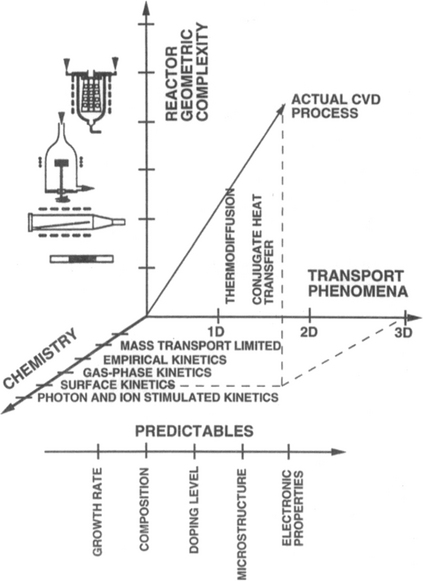
Figure 6-3 Schematic diagram of the chemical, transport, and geometrical complexities involved in modeling CVD processes.
(From Chemical Vapor Deposition, edited by M. L. Hitchman and K. F. Jensen. Reprinted with the permission of Academic Press, Ltd., and Professor K. F. Jensen, MIT.)
This chapter largely focuses on CVD processes that yield amorphous or polycrystalline films used in a variety of technologies. An exception is the treatment of epitaxial Si, a material well suited to model the thermodynamics and kinetics of film formation. Recommended books (Refs. 2-6) and review articles (Refs. 1, 7-10) dealing with these aspects of CVD are listed in the references. The very important CVD methods used to grow epitaxial III–V compound-semiconductor films for electronic and optoelectronics applications will be deferred to Chapter 8, however. In this way, corollary issues related to film crystallinity, stress, defects, and electrical properties can be better appreciated. Additional references reviewing these applications of CVD will be given then.
6.2 Reaction Types
To view the scope of the subject broadly, it is useful to first briefly categorize the various types of chemical reactions that have been employed to deposit films and coatings. Corresponding examples are given for each by indicating the essential overall chemical equation and approximate reaction temperature. In these equations (g) and (s) refer to gas and solid, respectively.
6.2.1 PYROLYSIS
Pyrolysis involves the thermal decomposition of such gaseous species as hydrides, carbonyls and organometallic compounds on hot substrates. Commercially important examples include the high-temperature pyrolysis of silane to produce polycrystalline or amorphous silicon films, and the low-temperature decomposition of nickel carbonyl to deposit nickel films:
Interestingly, the latter reaction is the basis of the Mond process, which has been employed for well over a century in the metallurgical refining of Ni.
6.2.2 REDUCTION
These reactions commonly employ hydrogen gas to effect the reduction of such gaseous species as halides, carbonyl halides, oxyhalides, or other oxygen-containing compounds. An important example is the reduction of SiCl4 on single-crystal Si wafers to produce epitaxial Si films according to the reaction
Refractory metal films such as W and Mo have been deposited by reducing the corresponding hexafluorides, e.g.,
Tungsten films deposited at low temperatures have served to interconnect levels of metallization in integrated circuits. Interestingly, WF6 gas reacts directly with exposed silicon surfaces depositing thin W films while releasing the volatile SiF4 by-product. In this way silicon contact holes can be selectively filled with tungsten while leaving neighboring insulator surfaces uncoated (see Section 6.8.6).
6.2.3 OXIDATION
Two examples of important oxidation reactions are:
The deposition of SiO2 by Eq. 6-6 is carried out at a stage in the processing of integrated circuits where higher substrate temperatures cannot be tolerated. Hard alumina coatings that extend the life of cutting tools are produced by reaction 6-7.
In another process of technological significance, a very pure form of SiO2 is produced by the oxidation reaction of Eq. 6-8:
The eventual application here is the production of optical fiber for communications purposes. Rather than a thin film, the SiO2 forms a cotton-candy-like deposit consisting of soot particles less than 1000 Å in size. These are then consolidated by elevated-temperature sintering to produce a fully dense silica rod for subsequent drawing into fiber. Whether silica films deposit or soot forms is governed by process variables favorable to heterogeneous or homogeneous nucleation, respectively. Homogeneous soot formation is essentially the result of a high SiCl4 concentration in the gas phase.
6.2.4 COMPOUND FORMATION
A variety of carbide, nitride, boride, etc., films and coatings can be readily produced by CVD techniques. What is required is that the compound elements exist in a volatile form and be sufficiently reactive in the gas phase. Examples of commercially important reactions for the deposition of hard, wear-resistant surface coatings include:
Films and coatings of compounds can generally be produced using a variety of precursor gases and reactions. For example, in the much-studied SiC system, layers were first produced in 1909 through reaction of SiCl4 + C6H6 (Ref. 11). Subsequent reactant combinations over the years have included SiCl4 + C3H8, SiBr4 + C2H4, SiCl4 + C6H14, SiHCl3 + CCl4, and SiCl4 + C6H5CH3, to name a few, as well as volatile organic compounds containing both silicon and carbon in the same molecule (e.g., CH3SiCl3, CH3SiH3, (CH3)2SiCl2). Although the deposit is nominally SiC in all cases, resultant properties generally differ because of structural, compositional, and processing differences.
Impermeable insulating and passivating films of Si3N4 are required to hermetically seal integrated circuits. Although they can be deposited at 750°C by the reaction
the necessity to deposit silicon-nitride films at lower temperatures has led to alternate processing involving the use of plasmas. Films can be deposited below 300°C with SiH4 and NH3 reactants, but considerable amounts of hydrogen are incorporated into the deposits.
The very important and rapidly growing metalorganic CVD (MOCVD) processes, used to deposit assorted epitaxial compound-semiconductor films, also fit under the present category of reactions. As the name implies, volatile organic precursor-compounds such as trimethylgallium (TMGa or (CH3)3Ga), trimethylindium (TMIn), etc., are employed. They are reacted with group V hydrides to form the semiconductor compound, e.g.,
Similar MOCVD reactions are exploited in producing a wide assortment of complex oxides and semiconductors, and these processes will be treated further in Sections 6.6.4 and 8.5.3.1, respectively.
6.2.5 DISPROPORTIONATION
Disproportionation reactions are possible when a nonvolatile metal can form volatile compounds having different degrees of stability depending on the temperature. This manifests itself in compounds, typically halides, where the metal exists in two valence states, e.g., GeI4 and GeI2, such that the lower-valent state is more stable at higher temperatures. As a result, the metal can be transported into the vapor phase by reacting it with its volatile, higher-valent halide to produce the more stable lower-valent halide. The latter disproportionates at lower temperatures to produce a deposit of metal while regenerating the higher-valent halide. This complex sequence can be simply described by the reversible reaction
and realized in systems where provision is made for mass transport between hot and cold ends. Elements which have lent themselves to this type of transport reaction include aluminum, boron, gallium, indium, silicon, titanium, zirconium, beryllium, and chromium. Single-crystal films of Si and Ge were grown by disproportionation reactions in the early days of CVD experimentation on semiconductors (Ref. 12) employing reactors like that shown in Fig. 6-4. The enormous progress made since then is evident.
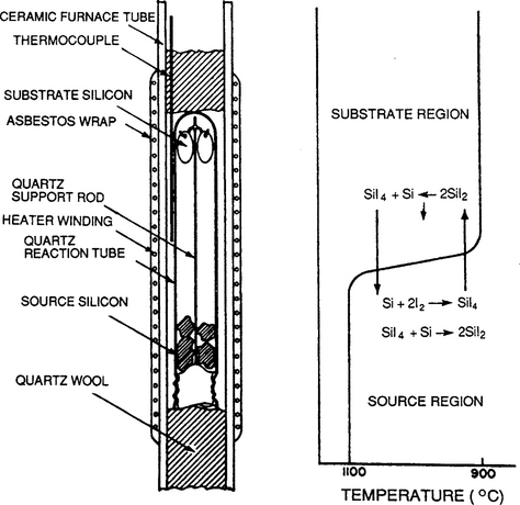
Figure 6-4 Early experimental reactor for epitaxial growth of Si films.
(From Ref. 12, copyright © 1960 by the IBM Corp., reprinted with permission.)
6.2.6 REVERSIBLE TRANSFER
Chemical transfer or transport processes are characterized by a reversal in the reaction equilibrium at source and deposition regions maintained at different temperatures within a single reactor. An important example is the deposition of epitaxial GaAs films by the chloride process according to the reaction
Here AsCl3 gas transports molten Ga, contained within the reactor, toward the substrates in the form of GaCl vapor. Subsequent reaction with As4 causes deposition of GaAs at low temperatures. At elevated temperatures the reaction reverses and the film is etched. In the alternative hydride process, As is introduced in the form of AsH3 (arsine) while HCl serves to transport Ga. Both processes essentially involve the same gas-phase reactions and are carried out in similar reactors. What is significant is that single-crystal, binary (primarily GaAs and InP but also GaP and InAs), ternary, e.g., (Ga, In)As and Ga(As, P), and quaternary epitaxial films containing controlled amounts of Ga, In, As, and P have been deposited by these processes. Combinations of gas mixtures, different substrates, and more complex reactors are required in these cases to achieve the desired film stoichiometries. These CVD processes have played an important role in fabricating the optoelectronic devices, e.g., lasers and detectors, that made long-distance optical communications possible. While they are still used, MOCVD processes are now supplanting these older CVD methods for depositing compound-semiconductor films.
The previous examples are but a small sampling of the total number of film and coating deposition reactions which have been researched in the laboratory as well as developed for commercial applications. In Table 6-1 there is a brief listing of CVD processes for depositing metals, semiconductors, and assorted compounds. Only inorganic source gases are noted here. (Metalorganic precursors and processes used to deposit these and other film materials will be discussed later.) The particular entries are culled from the review articles given earlier where specific details on process variables can be found.

In carefully examining the foregoing categories of CVD reactions, the discerning reader will note the following two common features:
1. All of the chemical reactions can be written in the simplified generalized form
where A, B… refer to the chemical species and a, b… to the corresponding stoichiometric coefficients. A single solid and mixture of gaseous species categorizes each heterogeneous reaction.
2. Some reactions are reversible, and this suggests that standard concepts of chemical thermodynamics may prove fruitful in analyzing them. Other reactions occur far from thermodynamic equilibrium and are strongly driven toward decomposition and film deposition.
There is a further distinction between chemical vapor deposition and chemical vapor transport reactions that should be noted. In the former, one or more gaseous species enter the reactor from gas tanks or liquid bubbler sources maintained outside the system. The reactants then combine at the hot substrate to produce the solid film. In chemical vapor transport reactions, solid or liquid sources are contained within either closed or open reactors. In this case externally introduced carrier or reactant gases flow over the sources, lifting them into the vapor stream where they are transported along the reactor. Subsequently, deposition of solid from the gas phase occurs at the substrates. Both chemical vapor deposition and transport reactions are, however, described by the same type of chemical reaction. As far as thermodynamic analyses are concerned, no further distinction will be made between them, and the generic term CVD will be used for both. We now turn our attention to the subject of thermodynamics.
6.3 THERMODYNAMICS OF CVD
6.3.1 REACTION FEASIBILITY
Thermodynamics addresses a number of important issues with respect to CVD. The question of whether a given chemical reaction is feasible or not is perhaps the most important of these. Once it is decided that a reaction is possible, thermodynamic calculation can frequently provide information on the partial pressures of the involved gaseous species and the direction of transport in the case of reversible reactions. Importantly, it provides an upper limit of what to expect under specified conditions. Thermodynamics does not, however, address questions related to the speed of the reaction and resulting film growth rates. Indeed, processes which are thermodynamically possible frequently proceed at such low rates because of both vapor transport kinetics and vapor–solid reaction limitations that they are unfeasible in practice. Furthermore, the use of thermodynamics implies that chemical equilibrium has been attained. Although this may occur in a closed system, it is generally not the case in an open or flow reactor where gaseous reactants and products are continuously introduced and removed. In general, CVD may be viewed as an empirical science with thermodynamic guidelines.
Provided that the free-energy change, ΔG, can be approximated by the standard free-energy change, ΔG0, many simple consequences of thermodynamics with respect to CVD can be understood. For example, consider the selection of suitable chemical reactions in order to grow single-crystal films. In this case, it is essential that a single nucleus form as an oriented seed for subsequent growth. According to elementary nucleation theory, a small negative value of ΔGV, the chemical free energy per unit volume, is required to foster a low nucleation rate of large critical-sized nuclei (Section 1.7). This, in turn, would require a ΔG0 value close to zero. When this happens, large amounts of reactants and products are simultaneously present. If ΔGv (i.e., ΔG°) were large and negative, however, the likelihood of a high rate of heterogeneous nucleation, or even homogeneous nucleation of solid particles within the gas phase, would be enhanced. The large driving force for chemical reaction tends to promote polycrystal formation in this case.
As an illustrative example it is worthwhile to follow the thought processes involved in the design of a CVD reaction to grow crystalline Y2O3 films. Following the treatment by Laudise (Ref. 13) consider the reaction
At 1000 K, ΔG° = −59.4 kcal/mol, corresponding to an equilibrium constant (Keq) given by log Keq = +13. The reaction is thus too far to the right for practical film growth. If the chloride is replaced by a bromide or iodide, the situation will be worse. YBr3 and YI3 are expected to be less stable than YCl3, making ΔG° even more negative. The situation is improved by adding a gas-phase reaction with a positive value of ΔG°, e.g.,
Thus, the possible overall reaction is now
for which ΔG° = –59.4 + 3(46.7) = +80.7 kcal/mol. The equilibrium now falls too far to the left, but substituting Y Br3 and Br2 for YCl3 and Cl2 changes the sign of ΔG° once again. Thus for
ΔG° = –27 kcal/mole. Although a value of ΔG° closer to zero would be more desirable, this reaction yields partial pressures of YBr3 equal to 10−2 atm when the total pressure is 2 atm. Growth in other systems has occurred at such pressures. Pending availability of YBr3 in readily volatile form and questions related to the operating temperature, reaction rates, and safety of gas handling, Eq. 6-20 appears to be a potential candidate for successful film growth. For analysis of chemical reactions good values of thermodynamic data are essential. Several sources of this information are listed among references E in Chapter 1.
6.3.2 CONDITIONS OF EQUILIBRIUM
Thermodynamics can provide us with much more than a prediction of whether a reaction will proceed or not. Under certain circumstances, it can yield quantitative information on the operating intensive variables which characterize the equilibrium. The problem is to evaluate the partial pressures or concentrations of the involved species within the reactor given the reactant compositions and operating temperature. In practice, the calculation is frequently more complicated than initially envisioned because in situ mass-spectroscopic analysis of operating reactors has surprisingly revealed the presence of unexpected species which must be accounted for. For example, in the technologically important deposition of epitaxial Si films on silicon wafer substrates, no fewer than eight gaseous compounds have been identified during the reduction of chlorosilanes. They are part of the much-studied Si–Cl–H system, and the following example illustrates the method of calculation (Refs. 14, 15). The most abundant chemical species in this system are SiCl4, SiCl3H, SiCl2H2, SiClH3, SiH4, SiCl2, HCl, and H2. Partial pressures of these eight gaseous species are connected by the following six equations of chemical equilibrium.
Throughout the activity of solid Si, aSi will be taken to be unity.
To solve for the eight partial pressures, two more equations relating these unknowns are required. The first specifies that the total pressure in the reactor, equal to the sum of the individual partial pressures, is fixed, e.g., at 1 atm. Therefore,
The final equation involves the Cl/H molar ratio, which may be taken to be fixed if there is no net change in the concentrations of Cl and H. Therefore,
The numerator represents the total amount of Cl in the system and is equal to the sum of the Cl contributed by each species. For example, the mass of Cl in SiCl4 is given by mCl = 4MCl (mSiCl4/MSiCl4) where m and M refer to the mass and molecular weight, respectively. But, by the perfect gas law,
Therefore, the number of moles of Cl = mCl/MCl or 4PSiCl4V/RT, and similarly for all other terms in the numerator and denominator. The common factor V/RT, involving the volume V and the temperature T of the reactor, cancels out and all that is left is given by Eq. 6-23.
There are now eight independent equations relating the eight unknown partial pressures which can be determined, at least in principle. First, however, the individual equilibrium constants Ki must be specified, and this requires a slight excursion requiring additional thermodynamic calculation. Ki is fixed by specifying T and ΔG°. A convenient summary of thermodynamic data in the Si–Cl–H system is given in Fig. 6-5 where the free energies of compound formation are plotted versus temperature in an Ellingham-type diagram. Each line represents the equation ΔG° = ΔH°–TΔS°, from which ΔH°, ΔS°, and ΔG° can be calculated at any temperature for the particular compound in question. For example, consider the formation reactions for SiCl4 and HCl at 1500 K. From Fig. 6-5,

Figure 6-5 Free energies of formation of important gaseous species in the Si-Cl-H system in the temperature range 800–1600 K.
(Reprinted with permission from the publisher, The Electrochemical Society, from Ref. 14.)

Therefore K1 = exp–6000/(1.99)1500 = 0.13, and similarly for other values of K.
The results of the calculation are shown in Fig. 6-6 for the case of a molar ratio of [Cl]/[H] = 0.01, which is typical of conditions used for epitaxial deposition of Si. Through application of an equation similar to 6-23, the molar ratio of [Si]/[Cl] was obtained and is schematically plotted in the same figure. A reactor operating temperature in the vicinity of 1400 K is suggested, because as a result of film deposition the Si content in the gas phase is minimized. Such temperatures are employed in practice. Analogous calculations have also been made for the case where [Cl]/[H] = 0.1, which is typical of conditions favoring deposition of polycrystalline Si. At equivalent temperatures the [Si]/[Cl] ratios are somewhat higher than obtained for epitaxial deposition, reflecting the greater Si gas concentration operative during polycrystal growth. In both cases hydrogen is by far the most abundant species in the gas phase.
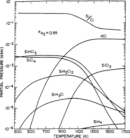
Figure 6-6 Equilibrium compositions of the SiCl4/H2 gas phase as a function of reactor temperature. Total pressure = 1 atm, Cl/H = 0.01.
(Reprinted with permission from the publisher, The Electrochemical Society, from Ref. 14.)
Now that a very laborious, traditional thermodynamic analysis of this multicomponent system has been presented, the reader will be relieved to know that there are now far simpler ways to compute the same results. In fact, by using the Outokumpu HSC Chemisty, computer-based thermodynamics database and computation software (Outokumpu Research Oy, P.O. Box 60, Fin-28101 Pori, Finland), the results of Fig. 6-6 can be reproduced in a matter of minutes. As another example, by means of this or other similar software, the equilibrium partial pressures of gas species participating in the reduction of CH4 by H2 were determined as a function of temperature. The results are shown in Fig. 6-7 and have been used as a guide in the synthesis of diamond films (Ref. 16).

6.4 GAS TRANSPORT
6.4.1 INTRODUCTION
Gas transport is the process by which volatile species flow from one part of a reactor to another. It is important to understand gas transport phenomena in CVD systems for the following reasons:
1. The deposited film or coating thickness uniformity depends on the delivery of equal amounts of reactants to all substrate surfaces.
2. Rapid deposition growth rates are dependent on optimizing the flow of reactants through the system and to substrates.
3. More efficient utilization of generally expensive process gases can be achieved as a result.
4. Computer modeling of CVD processes will be more accurate enabling improved reactor design and better predictive capability with regard to performance.
At the outset it is important to distinguish between diffusion and bulk flow processes in gases. Diffusion involves the motion of individual atomic or molecular species, whereas in bulk transport processes such as viscous flow or convection, parts of the gas move as a whole. Different driving forces and resulting transport equations define and characterize these two broad types of gas flow. Each of these will now be discussed briefly as a prelude to considering the flow combinations that take place in actual CVD reactors.
6.4.2 VISCOUS FLOW
The viscous flow regime is operative when gas transport occurs at pressures of roughly 0.01 atm and above in reactors of typical size. This is the pressure range characterisic of most CVD systems. At typical flow velocities of tens of centimeters per second, the reactant gases exhibit what is known as laminar or streamline flow. The theory of fluid mechanics provides a picture of what occurs under such circumstances. We shall consider the simplest of flow problems, i.e., that parallel to a flat plate. As shown in Fig. 6-8, the flow velocity has a uniform value ν0, but only prior to impinging on the leading edge of the plate. However, as flow progresses, velocity gradients must form because the gas clings to the plate. Far away the velocity is still uniform but drops rapidly to zero at the plate surface, creating a boundary layer. The latter grows with distance along the plate and has a thickness δ(x) given by δ(x) = 5x/(Rex)1/2, where Rex is the Reynolds number defined as Rex = υ0ρx/η. The quantities η and ρ are the gas viscosity and density, respectively. More will be said about η, but here it should be noted that the viscosity essentially establishes the frictional viscous forces which decelerate the gas at the plate surface.

Figure 6-8 Laminar gas flow patterns. (Top) Flow across flat plate. (Bottom) Flow through circular pipe.
The average boundary layer thickness over the whole plate is
 (6-24)
where ReL is defined as ReL = η0ρL/η. Because both gaseous reactants and products must pass through the boundary layer separating the laminar stream and film deposit, low values of d are desirable in enhancing mass-transport rates. This can be practically achieved by increasing the gas flow rate (v0), which raises the value of Re. Typical values of Re in CVD reactors range up to a few hundred. If, however, Re exceeds approximately 2100, a transition from laminar to turbulent flow occurs. The resulting erratic gas eddies and swirls are not conducive to uniform, defect-free film growth and are to be avoided.
It is instructive to now consider gas flow through a tube of circular cross section. The initial uniform axial-flow velocity is altered after the gas enters the tube. Boundary layers develop at the walls and grow with distance along the tube as shown in Fig. 6-8. The Reynolds number is now given by ∼2v0ρr0/η, where r0 is the tube radius. Beyond a certain critical entry length, Le ![]() , the flow is fully developed and the velocity profile no longer changes. At this point, the boundary layers around the tube circumference have merged and the whole cross section consists of “boundary layer.” The resulting axial flow is now described by the Hagen–Poiseuille relation
, the flow is fully developed and the velocity profile no longer changes. At this point, the boundary layers around the tube circumference have merged and the whole cross section consists of “boundary layer.” The resulting axial flow is now described by the Hagen–Poiseuille relation
where ![]() is the volumetric flow rate and ΔP/Δx is the pressure gradient driving force for viscous flow. Defined as the volume of gas which moves per unit time through the cross section, the volumetric flow rate is related to the average gas velocity
is the volumetric flow rate and ΔP/Δx is the pressure gradient driving force for viscous flow. Defined as the volume of gas which moves per unit time through the cross section, the volumetric flow rate is related to the average gas velocity ![]() by
by ![]() . Within the tube the gas velocity, v(r), assumes a parabolic profile as a function of the radial distance r from the center given by v(r) = vmax(1–r2/r2), where vmax is the maximum gas velocity. The gas flux J is given by the product of the concentration of the species in question and the velocity with which it moves:
. Within the tube the gas velocity, v(r), assumes a parabolic profile as a function of the radial distance r from the center given by v(r) = vmax(1–r2/r2), where vmax is the maximum gas velocity. The gas flux J is given by the product of the concentration of the species in question and the velocity with which it moves:
Upon substitution of Ci = Pi/RT from the perfect gas law, and ![]() ,
,
Provided the molar flux of any gaseous species in a chemical reaction is known, and equilibrium conditions prevail, the fluxes of other species can be determined from the stoichiometric coefficients.
Viscous flow is characterized by the coefficient of viscosity η. Kinetic theory of gases predicts that η varies with temperature as T1/2 but is independent of pressure. Experimental data bear out the lack of a pressure dependence at least to several atmospheres, but indicate that η varies as T” with n having values between 0.6 and 1.0. Gas viscosities measured in poise (P) typically range between 0.01 centipoise (cP) at 0°C and 0.1 cP at 1000°C. (1P = 0.1 Pa-s = 1 dyne-s/cm2.)
6.4.3 DIFFUSION IN GASES
The phenomenon of diffusion applies to mass transport in gases as well as condensed phases. In the case of two different gases that are initially separated and then allowed to mix, each will interdiffuse and increase the entropy of the system. Elementary kinetic theory of gases predicts that the diffusivity in gases depends on pressure and temperature as D∼T3/2/P. It is therefore usual to represent D in gases by
where n is experimentally found to be approximately∼1.8. D0, the value of D measured at standard temperature, T (273 K), and pressure, P (1 atm), is dependent on the particular gas combination in question. Typical D0 values at temperatures of interest span the range 0.1–10 cm2/s. Thus, diffusivity values in gases are many orders of magnitude higher than even the largest D values in solids. If the gas composition is reasonably dilute so that the perfect gas law applies for a given species i, Ci = Pi/RT and Eq. 1-22 can be equivalently expressed by
This formula can be applied to the diffusion of gas through the stagnant boundary layer of thickness d adjacent to the substrate. The flux is then given by
where pg is the vapor pressure in the bulk gas and Ps is the vapor pressure at the substrate surface.
Since D varies inversely with pressure, gas mass-transfer rates can be enhanced by reducing the pressure in the reactor. Advantage of this fact is taken in low-pressure CVD (LPCVD) systems, which are now extensively employed in semiconductor processing. Their operation will be discussed later in Section 6.6.3.
6.4.3.1 Close-Spaced Vapor Transport
As an example that integrates both thermodynamics and diffusion in a CVD process, consider the deposition of CdTe films by close-spaced vapor transport (CSVT) (Ref. 17). In this process mass is transferred from a solid CdTe source at temperature T1 located a very short distance l (typically 1mm) from the substrate maintained at T2 (T1 > T2). The present objective is to establish conditions necessary to derive an expression for the film growth rate. It is assumed that chemical equilibrium prevails at the respective temperatures. The basic reaction is
for which ΔG° = 68.64–44.94 × 10⁻³T kcal/mol. Therefore, the two equations
and
express the equilibria at source and substrate. If the concentrations of the gas phase species vary linearly with distance, the individual mass fluxes (in units of mol/cm2-s) are expressed by
Note the use of the perfect gas law and the neglect of the temperature dependence of D. Maintenance of stoichiometry requires that
the factor of 2 arising because Te2 is a dimer. The film growth rate is obtained by the relation
where M and ρ are the molar mass and density of CdTe, respectively. If T1 exceeds T2 by approximately 100°C, then Pi(T1) ![]() Pi(T2) where i refers to both Cd and Te2. By neglecting the T2 terms in Eqs. 6-33a and 6-33b,
Pi(T2) where i refers to both Cd and Te2. By neglecting the T2 terms in Eqs. 6-33a and 6-33b,
The value of 1.1 is derived from kinetic theory of gases, which suggests that DCd = 1.85 DTe2 in H2, or Ar ambients. Equations 6-32, 6-33, 6-34, and 6-36 enable all the partial pressures to be determined. By knowing the value of either DCd or DTe2, ![]() may then be determined.
may then be determined.
The technique of CSVT for semiconductor film growth has been reviewed by Perrier and Philippe (Ref. 18) and more recently applied to epitaxial SiC film growth (Ref. 19). Growth conditions in this study included source temperatures over 1900°C, 1–50 torr, a temperature gradient of 3.5°C/mm, and a source–substrate spacing of 1.5 mm.
6.4.4 CONVECTION
Convection is a bulk gas-flow process that can be distinguished from both diffusion and viscous flow. Whereas gas diffusion involves the statistical motion of atoms and molecules driven by concentration gradients, convection arises from the response to gravitational, centrifugal, electric, and magnetic forces. It is manifested in CVD reactors when there are vertical gas-density or temperature gradients. An important example occurs in cold-wall reactors such as depicted in Fig. 6-15 where heated susceptors are surrounded above as well as on the sides by the cooler walls. Cooler, more dense gases then lie above hotter, less dense gases. The resultant convective instability causes an overturning of the gas by buoyancy effects. Subsequently, a complex coupling of mass and heat transfer serves to reduce both density and temperature gradients in the system. Another example of convective flow occurs in two-temperature-zone vertical reactors. In the disproportionation process considered previously in Fig. 6-4, it is immaterial whether the hotter zone is physically located above or below the cooler zone insofar as thermodynamics is concerned. But efficient gas flow considerations mandate the placement of the cooler region on top to enhance gas circulation.

Figure 6-15 Schematic diagrams of reactors employed in epitaxial Si deposition. (Top) Horizontal; (lower left) pancake; (lower right) barrel.
(From S. M. Sze, Semiconductor Devices: Physics and Technology, copyright © 1985, John Wiley & Sons. Reprinted with permission.)
It is important to note that film growth is limited by viscous, diffusive, and convective mass transport fluxes which, in turn, are driven by gas pressure gradients. In open reactors the metered gas (volumetric) flow rates establish these pressure gradients. In closed reactors the latter arise because of imposed temperature differences which locally alter equilibrium partial pressures.
6.4.5 MODELING COMPLEX GAS TRANSPORT EFFECTS
When gas transport is physically more complex because of combined flows in three dimensions, the fundamental equations of fluid dynamics become the starting point of the analysis. Although there are standard treatments of the mathematical theory of transport phenomena, the texts by Lee (Ref. 20) and Middelman and Hochberg (Ref. 21) are recommended because of their chemical-engineering approach to CVD processing. Without delving into a detailed formal analysis it is instructive to note some of the features of the involved formidable partial differential equations. Three basic equations describing the conservation of mass, momentum, and energy provide the foundation of the subject. They are simply enumerated with brief verbal descriptions:
1. Continuity. The conservation of mass requires that the net rate of mass accumulation in a region be equal to the difference between the rate of mass flow in and out.
2. Navier–Stokes. Momentum conservation requires that the net rate of momentum accumulation in a region be equal to the difference between the rate of momentum in and out, plus the sum of forces acting on the system.
3. Energy. The rate of accumulation of internal and kinetic energy in a region is equal to the net rate of internal and kinetic energy in by convection, plus the net rate of heat flow by conduction, minus the rate of work done by the fluid.
In multicomponent fluid systems there are additional equations that describe concentration changes due to thermal and mass transport, as well as chemical reactions involving each of the species.
In principle, all of the above coupled equations together with the boundary conditions are sufficient to describe gas transport in reactors. However, in practice exact solutions are rare and only exist in the simplest cases, e.g., the isothermal tubular reactor of Sections 6.4.2. For this reason numerical methods based on finite-element analysis are often used to analyze gas flow in reactors of complex geometry where steep temperature gradients exist. Before starting, however, it is often found to be very useful to transform the equations into dimensionless forms by scaling the variables and properties that describe gas behavior relative to reference values. As a result, certain dimensionless numbers that may be interpreted as a ratio of the magnitude of two physical phenomena emerge in the equations.
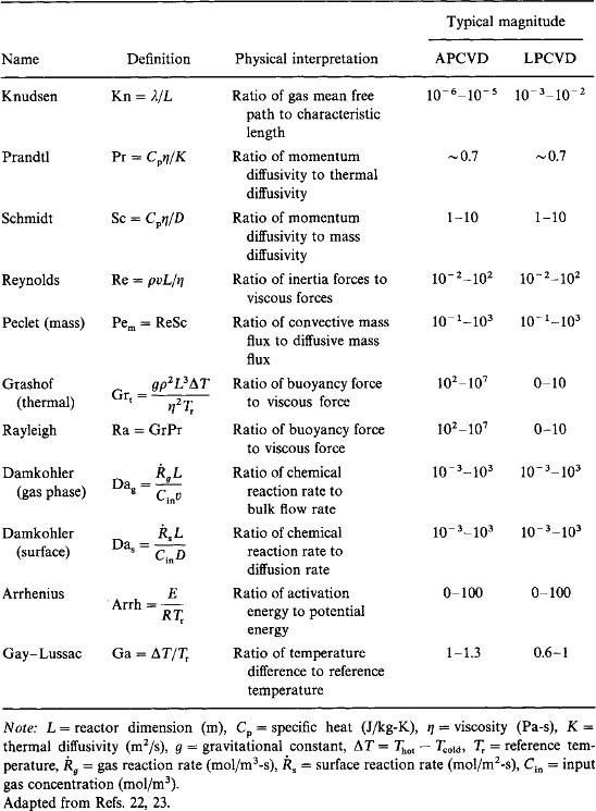
These as well as other useful dimensionless groups are defined in Table 6-2 together with their interpretations and typical magnitudes in atmospheric pressure (APCVD) and low-pressure (LPCVD) reactors (Refs. 22, 23). Although only Damkohler numbers Dag and Das specifically refer to chemical reaction rates among species within the gas or at the substrate surface, the other dimensionless groups describe gas transport in both multicomponent and homogeneous systems. In particular, the Peclet, Grashof/Rayleigh, Reynolds, Damkohler, and Knudsen numbers are important descriptors of CVD reactor processes. For example, when the Peclet number is large, species transfer is mainly due to convection, and downstream reaction products and impurities will not diffuse back to the reaction zone; for small Peclet numbers, transport due to diffusion dominates the flow. Large Grashof/Rayleigh numbers favor natural convection which tends to disturb the flow field. When the surface Damkohler number is large the film deposition process will be diffusion limited (see Section 6.5.3), but when the reverse is true surface-reaction limited deposition occurs. If the gas-phase Damkohler number is large, chemical reactions will proceed rapidly to establish thermodynamic equilibrium within the gas; but for small Damkohler numbers the residence time in the reactor is too short for gas-phase reactions to occur and the system will be far from equilibrium.
The following computer simulation of gas flow in a cylindrically symmetrical cold-wall, single-wafer reactor due to Kleijn (Ref. 23) provides an instructive application. This LPCVD reactor, containing radially impinging gas jets, was used to develop a process for depositing tungsten on 20-cm diameter silicon wafers through reduction of WF6 by H2. Subsequent figures depicted in Figs. 6-9a, 6-9b, and 6-9c illustrate the interplay of the dimensionless groups Re and Gr, at fixed Pr (Pr = 0.7) and Ga (Ga = 0.8) numbers. The resultant gas flow is expressed in terms of streamlines (ψ). Curves of ψ ranging from 0 to 1 represent the paths followed by “particles” of fluid, while gradients normal to the stream flow lines are measures of the gas velocity. Corresponding gas isotherms are also depicted. From these figures it is clear that increasing Gr at constant

Figure 6-9 Gas streamlines (left) over the range 0-1, and corresponding isotherms in K (right) for different combinations of Reynolds and Grashof numbers. The reactor profile is outlined. (a) Re = 1, Gr = 30; (b) Re = 1, Gr = 300; (c) Re = 10, Gr = 300.
(From C. R. Klerjn, “Transport Phenomena in Chemical Vapor Deposition Reactors.” Ph.D. Thesis, Technical University of Delft, 1991. Reprinted with permission.)
Re causes buoyancy-induced recirculation of gas near the edge of the heated susceptor, which then rises above it and finally falls at the cold reactor wall. However, the temperature profiles are relatively unaffected. Increasing Re suppresses the buoyancy-induced gas recirculation, produces inertial gas rolls, and creates a relatively thin thermal boundary layer above the wafer (horizontal). Clearly such simulations have the potential for suggesting reactor conditions that minimize undesirable buoyancy and inertial rolls and promote uniform flow across the wafer. Streamlining the reactor is effective in the latter regard.
6.5 FILM GROWTH KINETICS
The growth kinetics of CVD films is dependent on a number of factors associated with transport of reactants to the substrate surface and the subsequent heterogeneous surface reactions that lead to film formation. Intimate microscopic details of these reactions are often unknown and, therefore, the growth kinetics is frequently modeled in macroscopic terms. This is a simpler approach since it makes no atomistic assumptions, yet is capable of predicting deposit growth rates and uniformity.
6.5.1 AXIAL GROWTH-RATE UNIFORMITY
In this and the next section we treat the analysis of film growth on substrates placed in a horizontal reactor. We first consider the film thickness deposition rate on substrates lying parallel to the reactor axis, as a function of distance (Ref. 24). For the reactor configuration shown in Fig. 6-10a, the following is assumed:
1. The whole system is at constant temperature.
2. Along the reactor axis the gas has a constant velocity component.
3. The reactor extends a large distance in the z direction so that the problem reduces to one of two dimensions.
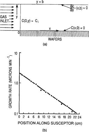
Figure 6-10 Horizontal reactor geometry with conditions for flow. (b) Variation of growth rate with position along susceptor. Reactor conditions: ![]() = 7.5 cm/s, b = 1.4 cm, T = 1200°C, and Ci = 3.1 × 10⁻⁵ g/cm3.
= 7.5 cm/s, b = 1.4 cm, T = 1200°C, and Ci = 3.1 × 10⁻⁵ g/cm3.
(From P. C. Rundle, Int. J. Electron. 24, 405,©1968 Taylor and Francis, Ltd.)
Furthermore, the flow is simply treated by assuming the mass flux J vector at any point to be composed of two terms involving the gas phase concentration of the depositing species, C(x, y),
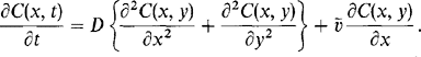
Whereas the first represents a bulk (plug) flow where the source gas moves as a whole with drift velocity v, the second term is due to diffusion of individual gas molecules, with diffusivity D, along concentration gradients. By taking the difference of the mass flux into and out of an elemental volume and equating it to the mass accumulation we obtain
 (6-38)
Only the steady-state solutions are of concern so that ![]() . The resulting equation is then subject to three conditions noted in Fig. 6-10a. Boundary value problems of this kind are readily solved by the well-known techniques of partial differential equations involving separation of variables or Laplace-transform methods. The solution is
. The resulting equation is then subject to three conditions noted in Fig. 6-10a. Boundary value problems of this kind are readily solved by the well-known techniques of partial differential equations involving separation of variables or Laplace-transform methods. The solution is
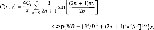 (6-39)
To obtain a more readily usable form of the solution, it is assumed as a first approximation that ![]() . Except for short distances into the reactor or small values of x, only the first term in the series need be retained. These simplifications yield
. Except for short distances into the reactor or small values of x, only the first term in the series need be retained. These simplifications yield
a solution whose concentration dependence is sinusoidal in the y direction and decays exponentially along x. The flux of source gas to the substrate surface is defined by
What we are after is the resultant deposit growth rate, ![]() Aside from simple material constants, this quantity is directly proportional to J(x)by
Aside from simple material constants, this quantity is directly proportional to J(x)by ![]() , where M and Ms are the molecular weights of the depositing species (Si) and source gas, respectively, and ρ is the film density. A combination of equations yields
, where M and Ms are the molecular weights of the depositing species (Si) and source gas, respectively, and ρ is the film density. A combination of equations yields
Values for D, ![]() , and Ci are strictly those pertaining to the mean temperature of the reactor, T. An exponential decay in the growth rate with distance along the reactor is predicted. This is not too surprising since the input gases are progressively depleted of reactants. The implicit boundary condition requiring that C = 0 at x = ∞ accounts for this loss. Despite the extreme simplicity of the assumptions, the model provides rather good agreement with experimental data on the variation of Si film growth rate with reactor distance as indicated in Fig. 6-10b. Although the specific reaction considered is the hydrogen reduction of chlorosilane, the results can be broadly applied to other CVD processes as well.
, and Ci are strictly those pertaining to the mean temperature of the reactor, T. An exponential decay in the growth rate with distance along the reactor is predicted. This is not too surprising since the input gases are progressively depleted of reactants. The implicit boundary condition requiring that C = 0 at x = ∞ accounts for this loss. Despite the extreme simplicity of the assumptions, the model provides rather good agreement with experimental data on the variation of Si film growth rate with reactor distance as indicated in Fig. 6-10b. Although the specific reaction considered is the hydrogen reduction of chlorosilane, the results can be broadly applied to other CVD processes as well.
From the standpoint of reactor performance, high growth rates and uniform deposition are the two most important concerns, assuming film quality is not comprised. The equation for ![]() serves to provide design guidelines, but these are not always simple to implement. Earlier it was noted that the boundary layer increased in the axial direction. To compensate for this effect and improve growth uniformity, d must be correspondingly reduced. Tilting the susceptor as shown in Fig. 6-15 is an effective remedy because the velocity of gas flow in the tapered space above the substrates is forced to increase with distance. Commercial horizontal and barrel reactors are designed with tilted susceptors so that enhanced transport across the stagnant layer compensates for reactant depletion. Continuously increasing the temperature downstream within the reactor is another way to enhance deposition uniformity.
serves to provide design guidelines, but these are not always simple to implement. Earlier it was noted that the boundary layer increased in the axial direction. To compensate for this effect and improve growth uniformity, d must be correspondingly reduced. Tilting the susceptor as shown in Fig. 6-15 is an effective remedy because the velocity of gas flow in the tapered space above the substrates is forced to increase with distance. Commercial horizontal and barrel reactors are designed with tilted susceptors so that enhanced transport across the stagnant layer compensates for reactant depletion. Continuously increasing the temperature downstream within the reactor is another way to enhance deposition uniformity.
6.5.2 RADIAL GROWTH-RATE UNIFORMITY ON WAFERS
In LPCVD reactors, silicon wafers are often stacked vertically along the tube axis and gases flow around and between them as shown schematically in Fig. 6-11a. The objective is to deposit polycrystalline and amorphous silicon films. In such cases it is not obvious that film thickness uniformity can be maintained across the wafer surface. Hitchman and Jensen (Ref. 25) have treated this problem whose analysis is more difficult than the one just considered. The reason is due to the more complex geometries of the wafer and their vertical stacking. Different gas flow and reaction in the interwafer spacing is thus established relative to the annular region between the tube walls and the periphery of the wafers. In the annulus, viscous flow or more simply plug flow may be assumed as previously. However, we are primarily interested in the interwafer region, where we shall assume the deposited film thickness depends solely on radial diffusional transport driven by compositional variations in the gas phase. Therefore, the steady-state diffusion equation in cylindrical coordinates for the circular wafers is
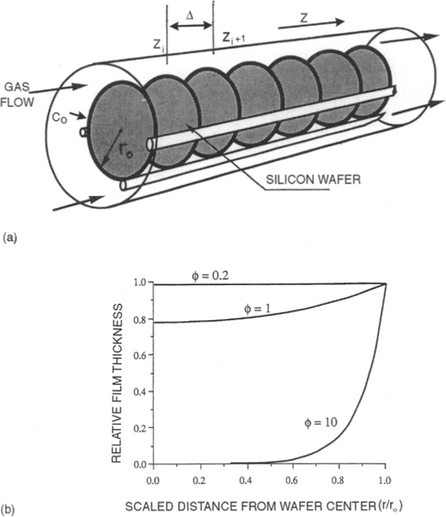
Figure 6-11 Schematic representation of hot-wall, multiple wafer LPCVD reactor geometry with gas flow boundary conditions. (b) Film thickness variation as a function of the scaled radial distance along the wafer for different values of φ.
(From Chemical Vapor Deposition, edited by M. L. Hitchman and K. F. Jensen. Reprinted with the permission of Academic Press, Ltd., and Professor K. F. Jensen, MIT.)
where r is the radial distance from the wafer center outward, and z is in the axial direction. The four boundary conditions are:
1. ![]() at r = 0 (because flow is axiosymmetric across the wafer).
at r = 0 (because flow is axiosymmetric across the wafer).
2. C = C0 at r = r0, where r0 is the wafer radius. (At r0, the gas concentration due to annular flow is joined to that of diffusion at the wafer edge.)
3. ![]() at z = zi. At the back surface (zi) of wafer i, the diffusional flux is consumed by a first-order chemical reaction whose rate constant is k.
at z = zi. At the back surface (zi) of wafer i, the diffusional flux is consumed by a first-order chemical reaction whose rate constant is k.
For a small wafer spacing (Δ) relative to r0 (typically Δ/r0 < 0.05), we may replace differentials by averages so that ![]() may be replaced by
may be replaced by ![]() , leaving
, leaving
The corresponding deposit growth rate on the wafer is again expressed by ![]() = MJ/ρMs, where now J —kC(r). Exact C(r)vs r solutions of Eq. 6-44 subject to boundary conditions 1 and 2 are in the form of incomplete Bessel functions of zero order, I0. A comparison of the film thickness (d)as a function of r relative to that at the wafer edge is instructive and given by
= MJ/ρMs, where now J —kC(r). Exact C(r)vs r solutions of Eq. 6-44 subject to boundary conditions 1 and 2 are in the form of incomplete Bessel functions of zero order, I0. A comparison of the film thickness (d)as a function of r relative to that at the wafer edge is instructive and given by
 (6-45)
Defining the dimensionless quantity ![]() when
when ![]() diffusion is rapid compared to surface reaction and the depositing species is uniformly distributed in the interwafer space; such conditions yields a uniform deposit. On the other hand when
diffusion is rapid compared to surface reaction and the depositing species is uniformly distributed in the interwafer space; such conditions yields a uniform deposit. On the other hand when ![]() , diffusion cannot keep up with the surface reaction and the precursor gas is depleted at the wafer center, resulting in a thinner deposit; a “bull’s-eye” effect now characterizes the nonuniform film thickness. These results are graphically illustrated in
, diffusion cannot keep up with the surface reaction and the precursor gas is depleted at the wafer center, resulting in a thinner deposit; a “bull’s-eye” effect now characterizes the nonuniform film thickness. These results are graphically illustrated in
6.5.3 TEMPERATURE DEPENDENCE
In order to understand the effect of temperature on film growth it is instructive to reproduce the classic treatment of film growth by Grove (Ref. 26). The essentials of this simple model are noted in Fig. 6-12 where the environment in the vicinity of the gas/growing film interface is shown. A drop in reactant concentration occurs from Cg in the bulk gas to Cg at the interface. The corresponding mass flux is given by
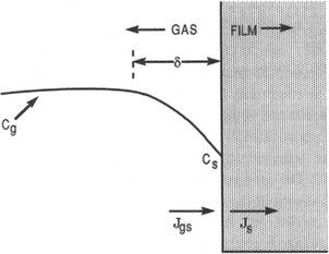
Figure 6-12 Model of CVD growth process. Gas flows normal to plane of paper.
(From Ref. 26. Reprinted with permission from John Wiley & Sons, copyright © 1967.)
where hg is the gas-phase mass-transfer coefficient to be defined later. The flux consumed by the reaction taking place at the surface of the growing film is approximated by
where first-order kinetics are assumed, and ks is the rate constant for surface reaction. In the steady state Jgs = Js and therefore,
This formula predicts that the surface concentration drops to zero if ![]() , a condition referred to as mass-transfer control. In this case slow gas transport through the boundary layer limits the otherwise rapid surface reaction. Conversely, surface-reaction control dominates when
, a condition referred to as mass-transfer control. In this case slow gas transport through the boundary layer limits the otherwise rapid surface reaction. Conversely, surface-reaction control dominates when ![]() , in which case Cs approaches Cg. Here the surface reaction is sluggish even though sufficient reactant gas is available. The film growth rate,
, in which case Cs approaches Cg. Here the surface reaction is sluggish even though sufficient reactant gas is available. The film growth rate,![]() , is given by
, is given by![]() , where
, where![]() is the atomic density or number of atoms incorporated into the film per unit volume. Therefore,
is the atomic density or number of atoms incorporated into the film per unit volume. Therefore,
The temperature dependence of ![]() hinges on the properties of ks and hg. A Boltzmann-like behavior dominates the temperature dependence of the surface chemistry, that is,
hinges on the properties of ks and hg. A Boltzmann-like behavior dominates the temperature dependence of the surface chemistry, that is, ![]() where E is the characteristic activation energy involved. Comparison of Eqs. 6-30 and 6-46 reveals that hg is related to D/d. Since Dg varies as T2 at most, and d is weakly dependent on T,hg is relatively insensitive to variations in temperature. At low temperatures, film growth is surface-reaction controlled, that is,
where E is the characteristic activation energy involved. Comparison of Eqs. 6-30 and 6-46 reveals that hg is related to D/d. Since Dg varies as T2 at most, and d is weakly dependent on T,hg is relatively insensitive to variations in temperature. At low temperatures, film growth is surface-reaction controlled, that is, ![]() whereas at high temperatures the gas mass-transfer or diffusion-controlled regime is dominant where
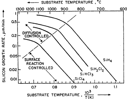
whereas at high temperatures the gas mass-transfer or diffusion-controlled regime is dominant where ![]() . The predicted behavior is borne out by growth rate data for epitaxial Si as shown in the Arrhenius plots of Fig. 6-13. Actual film growth processes are carried out in the gas diffusion-controlled region where the temperature response is relatively flat. At lower temperatures the same activation energy of about 1.5 eV is obtained irrespective of chlorosilane used. Migration of Si adatoms is interpreted to be the fundamental rate-limiting step in this temperature regime.
. The predicted behavior is borne out by growth rate data for epitaxial Si as shown in the Arrhenius plots of Fig. 6-13. Actual film growth processes are carried out in the gas diffusion-controlled region where the temperature response is relatively flat. At lower temperatures the same activation energy of about 1.5 eV is obtained irrespective of chlorosilane used. Migration of Si adatoms is interpreted to be the fundamental rate-limiting step in this temperature regime.
6.5.4 INFLUENCE OF THERMODYNAMICS
The previous discussion implies that all reaction rates increase with temperature. Although this is generally true, it is sometimes observed that higher reactor temperatures lead to lower film growth rates in certain systems. This apparent paradox can be explained by considering the reversibility of chemical reactions (Ref. (27). In Chapter 1 the net rate for a forward exothermic reaction (and reverse endothermic reaction) was given by Eq. 1-36 and modeled in Fig. 1-19. Recall that exothermic reactions mean that the sign of is negative, that is, the reactants have more energy than the products. For endothermic reactions, ΔH is positive. The individual forward and reverse reaction components are now shown in Fig. 6-14a on a common plot. Clearly, the activation energy barrier (or slope) for the reverse reaction exceeds that for the forward reaction. The net reaction rate or difference between the individual rates is also indicated. Interestingly, it reaches a maximum and then drops with temperature. A practical manifestation of this is etching–the reverse of deposition–in the high temperature range.
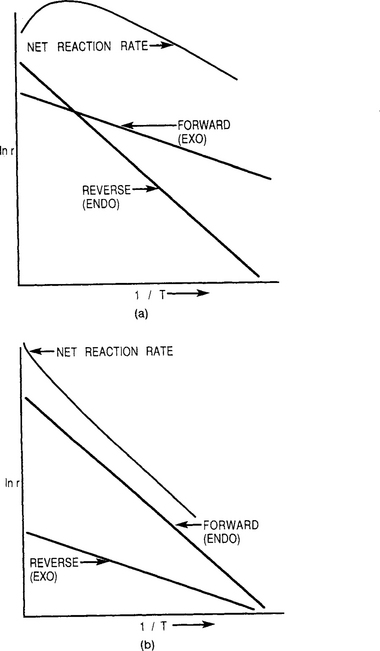
Figure 6-14 Chemical reaction energetics. (a) Activation energy for forward exothermic reaction is less than for reverse endothermic reaction. (b) Activation energy for forward endothermic reaction is greater than for reverse exothermic reaction.
(After Ref. 27.)
In Fig. 6-14b the alternate case is considered, that is, a forward endothermic deposition reaction and a reverse exothermic reaction. Here the net reaction rate increases monotonically with temperature and film growth rates will always increase with temperature. It is left for the reader to show that ΔH° for the reduction of SiCl4 by H2 (Eq. 6-3) is endothermic as written, for example, ![]() . There is actually a thermodynamic driving force which tends to transport Si from the cooler regions, the walls, to the hottest part of the reactor. This is where inductively heated substrates are placed and where film growth rates are highest. Epitaxial Si is most efficiently deposited in so-called cold-wall reactors for this reason.
. There is actually a thermodynamic driving force which tends to transport Si from the cooler regions, the walls, to the hottest part of the reactor. This is where inductively heated substrates are placed and where film growth rates are highest. Epitaxial Si is most efficiently deposited in so-called cold-wall reactors for this reason.
The opposite is true when ΔH < 0. Reversible reactions (Eq. 6-15) for the deposition of GaAs are exothermic and hot-wall reactors are employed in this case to prevent deposition on the walls. These results are a direct consequence of the well-known van’t Hoff equation
6.6 THERMAL CVD PROCESSES
6.6.1 SCOPE
The remainder of the chapter builds on the fundamentals of gas flow and reactions in CVD processes by describing their practical exploitation in producing films and coatings of interest. Most CVD processes can be conveniently subdivided into two categories. Thermal CVD processes employ heat energy to activate the required gas and gas-solid phase reactions. In contrast, the plasma-enhanced CVD processes treated in Section 6.7 derive benefit from plasma activation of the involved chemical species. As we shall see, however, even with similar input gases used to deposit the same nominal materials, films produced by thermal and plasma CVD processes can differ widely with respect to film structure, composition, and properties.
The great variety of materials deposited by thermal CVD methods has inspired the design and construction of an equally large number of processes and systems. Thermal processes have been broadly differentiated by such descriptors as low and high temperature, atmospheric and low pressure, cold and hot wall, and closed and open. Within a specific category of process, the variations in design and operating variables frequently make it difficult to compare performance of individual systems or reactors, even when depositing the same material. Regardless of process type, however, the associated equipment must have the following capabilities:
1. Deliver and meter the reactant and diluent gases into the reactor
2. Supply heat to the substrates so that reaction and deposition can proceed efficiently
In this section we will discuss some of the more widely practiced thermal CVD processes as well as some less common CVD methods; notably absent here is a treatment of CVD techniques for compound-semiconductor epitaxy, a subject extensively covered in Chapter 8. Since more information is published on CVD applications and equipment for microelectronic device fabrication, the subsequent discussion will reflect this reality.
6.6.2 ATMOSPHERIC-PRESSURE CVD
6.6.2.1 High-Temperature Atmospheric-Pressure Systems
Although there is a continual imperative to reduce semiconductor processing temperatures, the growth of high-quality epitaxial thin films is often achieved by high-temperature, atmospheric-pressure CVD (APCVD) methods. This is true of Si as well as compound semiconductors. The reactors employed can be broadly divided into hot-wall and cold-wall types. Three popular cold-wall reactor configurations are depicted in Fig. 6-15. Of note in both the horizontal and barrel reactors are the tilted susceptors. As previously discussed, this feature compensates for reactant depletion, which results in progressively thinner deposits downstream. In contrast to the other types, the wafer substrates lie horizontal in the pancake reactor. Incoming reactant gases flow radially over the substrates where they partially mix with the product gases.
Barrel reactors are commonly utilized for the deposition of epitaxial Si films where the reactions listed in Eqs. 6-21a-f occur. Silicon wafers are placed in good thermal contact with SiC-coated graphite susceptors which can be inductively heated while the nonconductive chamber walls are simultaneously air or water cooled. These reactors typically operate with H2 flow rates of several hundred standard liters per minute, and 1 vol% SiCl4. Silicon film growth rates of 0.2 to 3 μm per minute are attained under these conditions. Substantial radiant heat loss from the susceptor surface and consumption of large quantities of gas, 60% of which is exhausted without reacting at the substrate, limit the efficiency of these reactors.
High-temperature APCVD systems are also extensively employed in the deposition of hard metallurgical coatings (Refs. 5, 28). One of the important advantages of CVD methods is the ability to batch coat large numbers of small tools at one time. For this purpose commercial hot-wall reactor systems capable of individual or sequential TiC, TiN, and Al2O3 film depositions have been constructed as schematically indicated in Fig. 6-16a. Perhaps billions of cemented tungsten-carbide cutting tools have now been coated since the mid-1960s in such reactors. As many as 10–20,000 WC tool inserts (∼ 1 cm square) can be simultaneously given a∼6 μm thick coating during a several-hour treatment cycle at temperatures within the range 700–1100°C. Since hard coatings are deposited on varied substrates, such as carbides, high-speed tool steels, and ball-bearing steels, a wide range of substrate temperatures is required, necessitating different deposition techniques and conditions. For example, TiN can be deposited by CVD over a broad range of temperatures using the same TiCl4 precursor. Some typical reactions leading to the attractive, lustrous golden TiN deposits are:
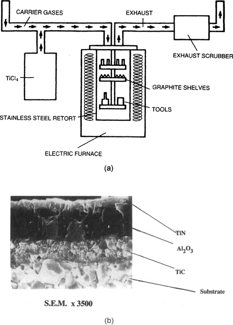
Figure 6-16 Schematic view of a commercial CVD reactor for deposition of TiC, TiN, and Al2O3 on carbide cutting tools.
(Courtesy of A. Gates, Multi-Arc Scientific Coatings Inc.) (b) SEM image of CVD multilayer coating for cutting tool inserts. Carbide substrate/TiC/Al2O3/TiN (3500 ×). Courtesy of S. Wertheimer, ISCAR Ltd.
1. High temperature, 1200°C > T > 850°C:
2TiCl4 + N2 + 4H2 → 2TiN + 8HCl
2. Moderate temperature, 850°C > T > 700°C:
TiCl4 + CH3CN + 5/2H2 → Ti(C, N) + CH4 + 4HCl
Deposition at temperatures as low as 300°C is possible, but this requires operation in a plasma discharge. Analogous reactions involving methane result in TiC deposits. The microstructure of such a multilayer CVD coating is shown in Fig. 6-16b.
6.6.2.2 Low-Temperature Atmospheric Pressure Processes
It has already been noted (Section 6.1) that in the fabrication of both memory and logic IC chips, assorted dielectric thin films, such as SiO2, BPSG glasses, and silicon nitride, are deposited in order to insulate, passivate, mask, or hermetically seal various parts of the underlying circuitry. Several types of atmospheric-pressure, low-temperature reactors have been devised over the years in order to deposit these films. They include resistance-heated rotary reactors of radial configuration and reactors featuring a close-spaced gas-nozzle geometry. In the latter, gases impinge on wafers translated past the nozzles on a metal conveyer belt. As we shall see subsequently, atmospheric CVD methods have been supplanted in many cases by low pressure CVD and plasma CVD processes; the former enable greater wafer throughputs while the latter promote film deposition at lower temperature.
The widely deployed SiO2 films have been deposited via the oxidation of silane
and the decomposition of tetraethyloxysilicate or TEOS (Si(OC2H5)4),
Instead of pyrophoric silane, the latter reaction employs an inert liquid precursor. Another advantage is the improved step and trench coverage with TEOS. This is due to the fact that the very reactive SiH4 decomposes immediately as it hits the surface. On the other hand the more complex TEOS molecules decompose slowly and diffuse further along the surface or down a trench before leaving SiO2 behind (Ref. 6). TEOS is widely used to produce the intermetal-dielectric filling in multilevel IC structures. Although APCVD (ozone/TEOS) and low-pressure CVD have been employed for this purpose (Ref. 29), the low-pressure, high-density plasma-assisted (O2-TEOS) CVD processes discussed in Section 6.7.3.1 appear to be the wave of the future (Ref. 30).
For the premetal dielectric layer that fills the space between the transistors and the first level of metallization (see Fig. 6-1), films of BPSG are traditionally employed (Ref. 31). This important layer has two functions. It electrically isolates transistors from the metal conductors, and protects them from being exposed to harmful Na+ and K+ ions, which degrade device performance. Containing about 2–6 wt% each of B and P, such films are deposited by thermal CVD methods at 500–700°C and annealed at 800–1000°C. When SiH4 is cooxidized with PH3, films of phosphosilicate glass (PSG) form, but reaction with PH3 + B2H6 mixtures generates BPSG. The role of phosphorus is to getter or trap the mobile ions, while boron “softens” the layer facilitating viscous flow and planarization during reflow annealing.
6.6.3 LOW-PRESSURE CVD (LPCVD)
One of the significant developments in semiconductor device processing was the introduction of CVD reactors that operate at lower than atmospheric pressure. Historically they were first employed to deposit polysilicon films for gate electrodes. However, assorted dielectric films such as SiO2, silicon oxynitrides, and silica glass, in addition to tungsten, other refractory metals, and silicide films, have also been deposited by LPCVD methods. If APCVD was capable of producing some of these films, what accounted for the adoption of LPCVD processing with its more complex reactors? The chief reason is the cost savings achieved by packing wafers more densely than is possible in APCVD. In practice, large batches of wafers, a hundred or more, can be processed at a time. This coupled with generally high deposition rates, improved film-thickness uniformity, better step coverage, greater control over stoichiometry and contamination problems, lower particle density, and fewer pinhole defects has given LPCVD important advantages in the processing of dielectric films.
Depending on how much below atmospheric pressure the CVD reactor operates, three different process regimes have been distinguished. From 100 torr to 1 torr we speak of reduced pressure CVD (RPCVD), while LPCVD is commonly practiced in the range from 1 to 10 mtorr. Ultrahigh vacuum CVD at∼10−7 torr, a subject discussed in Section 8.6.3.2, has enabled the realization of low-temperature silicon epitaxy. To compensate for low pressures of operation relative to 760 torr in APCVD reactors, the input reactant gas concentration must be correspondingly enriched to maintain comparable deposition rates. Actually, when normalized to the same reactant partial pressure, LPCVD film growth rates may indeed exceed those for conventional atmospheric CVD. Low gas pressures primarily enhance the mass flux of gaseous reactants and products through the boundary layer between the laminar gas stream and substrates. This effect on mass transport can be semiquantitatively estimated. According to Eq. 6-30 the mass flux of the gaseous species is directly proportional to D/δ. Since the diffusivity varies inversely with pressure, D is roughly 1000 times higher in the case of LPCVD. This more than offsets the increase in δ, which is inversely proportional to the square root of the Reynolds number. In an LPCVD reactor the gas-flow velocity is generally a factor of 10–100 times higher, the gas density a factor of 1000 lower, and the viscosity unchanged relative to APCVD. Therefore, Re is a factor of 10 to 100 times lower and δ about 3 to 10 times larger. Because the change in D dominates that of δ, a mass transport enhancement of well over an order of magnitude can be expected for LPCVD.
Now consider wafers in an APCVD reactor. Efficient film growth is limited by mass transport through the boundary layer of the flowing gases, and to overcome this barrier wafers are laid parallel to the gas stream. But in LPCVD reactors, gas molecules have a larger mean free path and greatly enhanced diffusivity. Gas will readily impinge on the wafers and deposition is no longer mass-transfer limited but rather reaction-rate controlled. This means that wafers can be stacked closer together and parallel to each other (Section 6.5.2), resulting in high wafer throughputs.
Commercial LPCVD systems commonly employ resistively heated, horizontal hot-wall reactors, as shown schematically in Fig. 6-11a. Big mechanical pumps as well as blower booster pumps are required to accommodate the large gas load at low operating pressures. One significant difference between atmospheric and LPCVD systems concerns the nature of deposition on reactor walls. Dense, adherent deposits accumulate on the hot walls of LPCVD reactors whereas thinner, less adherent films form on the cooler walls of atmospheric reactors. In the latter case, particulate detachment and incorporation in films is a problem especially on horizontally placed wafers. It is less of a problem for LPCVD reactors where vertical stacking is employed.
6.6.4 METALORGANIC CVD (MOCVD) PROCESSES
Originally developed by Manasevit and co-workers (Ref. 32) in the late 1960s to grow epitaxial compound semiconductor films MOCVD (also known as organometal, OMCVD) is now widely used for that purpose. But MOCVD has also assumed additional importance in the deposition of assorted dielectrics and metals as well. Unlike other CVD process variants that are differentiated physically on the basis of pressure, or use of plasmas or photons (see Section 6.6.5), MOCVD is distinguished by the chemical nature of the precursor gases. The great advantage of metalorganics is their generally high volatility at moderately low temperatures. Since all constituents are in the vapor phase, precise electronic control of gas flow rates and partial pressures is possible without dealing with troublesome liquid or solid sources in the reactor. This, combined with pyrolysis reactions which are relatively insensitive to temperature, allows for efficient and reproducible deposition. Carbon contamination of films is a disadvantage, however. MOCVD reactions are usually carried out at low pressures, and sometimes with plasma assist. The reactors employed, which are discussed more fully in Section 8.5.3.1, are carefully designed to optimize the flow and efficient use of generally expensive precursors.
It is useful to divide the discussion of MOCVD along two major lines of applications. The more important ones deal with epitaxial compound-semiconductor deposition, a subject that will be treated in Chapter 8. On the other hand applications considered here are to the deposition of oxide and metal films. In general, semiconductor deposition needs are more stringent with regard to reactor design and performance, as well as film quality.
At the top of Table 3-4 we have already noted a number of electroceramic films that have been prepared by pulsed-laser deposition. Because they include important applications in microelectronics, electrooptics, nonlinear optics, and information storage and display, there has been an imperative to prepare these materials by other methods including MOCVD. Assorted ferroelectric (Pb, Ba, Zr, Sr)TiO3 films, in particular, have been the subject of much attention (Refs. 33-35). By virtue of hysteresis effects in electric fields and two remanent polarization states, these titanates possess a natural memory. This, coupled with their very large dielectric constants, makes them obvious choices as capacitor dielectrics for high-density DRAM applications. In producing these films, precursors are typically heated to ∼200°C while deposition occurs anywhere from ∼300 to 1000°C. Amorphous as well as oriented microcrystalline films often deposit on silicon wafers; epitaxial films of BaTiO3 have been grown on LaAlO3 (Ref. 33).
Although the production of technologically significant surface areas of electroceramic films by laser ablation is not yet practical, MOCVD technology employing metal alkoxides or -diketonate precursors offers a flexible approach for depositing oxides (Ref. 36). MOCVD possesses the potential for large-area deposition, good composition control and film uniformity, high film-deposition rates and densities, and conformal step coverage. Success strongly hinges on the availability of suitable precursors; in this regard, commercial scale-up of MOCVD requires the following: (1) batch precursor amounts must rise from a few grams to a few kilograms, (2) production yields must rise and quality be consistent, (3) the environmental impact must be minimal, and (4) safety must be assured. Typical MOCVD precursors for electroceramic metal-oxide film deposition are listed in Table 6-3.

Before leaving this subject, it is worth noting a very versatile and inexpensive thin-film preparation method that employs metalorganic precursors in a novel way (Refs. 37, 38). Instead of being injected into a reactor as a gas, the precursors are directly applied to the substrate by spin coating, spraying, or dipping. Then a high-temperature treatment decomposes the compound, leaving the desired thin film behind. By this metalorganic decomposition (MOD) process, assorted oxide films such as SrTiO3 and YBa2Cu3O7 have been prepared. It is claimed that epitaxial films are sometimes obtained at very high decomposition temperatures.
6.6.5 LASER-ENHANCED CVD DEPOSITION
There is considerable interest in depositing thin films at selected locations on unpatterned or broad-area substrates. This can be achieved by focusing beams of photons, electrons, or ions that are scanned or made to pass through mask openings. Where these beams hit substrates immersed in a CVD environment, reactions are triggered, resulting in writing or initiation of deposition. Laser- or, more generally, photoassisted chemical processing involves the use of monochromatic light to enhance and control film deposition.
Two mechanisms are involved during laser-enhanced chemical-vapor deposition (LECVD) and these are illustrated in Fig. 6-17. In the pyrolytic mechanism the laser heats the substrate to decompose gases above it and enhance rates of chemical reactions there. Many different lasers are suitable for pyrolytic deposition. However, substrates that melt above the gas decomposition temperatures are required. Photolytic processes, on the other hand, depend on direct dissociation of molecules by energetic photons Organic metal dialkyl and trialkyl precursors are often used. Ultraviolet light sources are essential because many useful parent molecules (e.g., SiH4, Si2H6, Si3H8, N2O) require absorption of photons with wavelengths of less than 220 nm to initiate dissociation reactions. Practical lasers for this purpose are essentially the same as those employed for pulsed-laser deposition (Section 3.5.2.2) but operate at typical powers of a few tens of milliwatts. Such power levels are too low to enable high deposition rates over large areas, but are sufficient to initiate deposits selectively. It should be noted that there is frequently an admixture of pyrolytic and photolytic deposition processes occurring simultaneously with deep UV sources. Alternately, pyrolytic deposition is accompanied by some photodissociation of loosely bound complexes if the light source is near the UV.
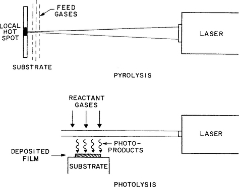
Figure 6-17 Pyrolytic and (b) photolytic laser-induced chemical-vapor deposition of films
(From Chemical Vapor Deposition, edited by M. L. Hitchman and K. F. Jensen. Reprinted with the permission of Academic Press, Ltd., and Professor K. F. Jensen, MIT.)
Photolytically deposited metals are usually contaminated with carbon and display poor conductivity. For this reason direct writing of materials is usually accomplished by pyrolytic processes. Metal films so deposited have been used to repair open circuit defects in integrated circuits as well as “clear” defects in lithographic masks (Ref. 39). A number of metals such as Al, Au, Cr, Cu, Ni, Ta, Pt, and W have been deposited by LECVD using assorted volatile metal carbonyls, hydrides, and metalorganic compounds (see Table 6-3). Results for several metals indicate what may be expected of LECVD.
1. Aluminum films with electrical resistivities 1.2 to 3 times that of bulk Al have been deposited at∼100°C from dimethylaluminum hydride and trimethylamine alane. Vertical film-growth rates up to 20 μm-s−1, while scanning at speeds of 600 μm-s−1, have been achieved.
2. Copper films of >95% purity, with resistivities of 2–2.2 μ Ω -cm, have been deposited at less than 200°C.
3. Gold films deposited at growth rates of 3 μ m-s−1, with resistivities 1.4–10 times that of bulk Au, have been derived from gold diketonate sources.
Additional information has been published on the CVD of metals, including deposition temperatures (Ref. 40) and selective deposition (Ref. 41).
Research on the photo-assisted deposition of elemental semiconductors (Si, Ge, diamond), compound semiconductors (GaAs, InP, GaP, HgTe, HgCdTe), dielectrics (SiO2, TiO2, silicon nitride) has been reviewed by McCrary and Donnelly (Ref. 42). As with metals, LECVD processing enables selective deposition of these materials at temperatures hundreds of degrees lower than possible by other methods. The exciting possibilities of low-temperature processing are offset by generally inferior film properties.
6.7 PLASMA-ENHANCED CVD PROCESSES
6.7.1 OVERVIEW
In PECVD processes, glow-discharge plasmas are sustained within chambers where simultaneous vapor-phase chemical reactions and film deposition occur. Just as the demands of semiconductor technology provided the driving force for advances in sputtering and plasma etching, PECVD processing arose from similar imperatives. A major early commercial application of PECVD was the low-temperature deposition of silicon nitride films for the passivation and encapsulation of completely fabricated microelectronic devices. At this final stage IC chips cannot be heated much above 300°C, a far lower temperature than that used in traditional thermal CVD processes for silicon-nitride deposition.
In the majority of PECVD processing activity, glow-discharge plasmas are excited by an RF field. The reason is that most films deposited by this method are dielectrics and DC discharges are not feasible. Generally, the RF frequencies employed range from about 100 kHz to 40 MHz. In the reduced gas pressure environment, typically sustained between 50 mtorr and 5 torr, electron and positive ion densities number between 109 and 1011/cm3, and average electron energies range from 1 to 10 eV. This energetic discharge is sufficient to decompose gas molecules into a variety of component species, i.e., ions, atoms and molecules in ground and excited states, molecular fragments, free radicals, etc. The net effect of the interactions among these reactive entities is to cause chemical reactions to occur at much lower temperatures than in thermal CVD reactors not benefiting from plasma activation. Therefore, previously unfeasible high-temperature reactions can be made to occur on temperature-sensitive substrates.
To illustrate that thermodynamic limitations are overcome by plasmas consider the formation of TiC by the reaction of Eq. 6-10, for which the free energy is given by ΔG° (kcal/mol) = 72–0.059T. The temperature that divides thermodynamically possible from impossible reaction occurs when ΔG°= 0, or 1218 K. Below this temperature ΔG° > 0 and no TiC ought to form, a conclusion in rough accord with the typical∼1000°C temperature for film deposition. However, in the presence of a plasma, the energy barrier for reaction is reduced and deposition occurs at 700 K (Ref. 43).
A sampling of assorted materials that have been deposited by PECVD methods is included in Table 6-4 together with typical operating temperatures and source gas compositions (Refs. 43, 44). Included are elements such as carbon in the form of diamond and diamond-like films, metals, oxides, nitrides, and borides. Although semiconductor films have been prepared by PECVD, their stoichiometry and crystalline quality are simply insufficient for device purposes.
Table 6-4 PECVD Films, Source Gases, and Deposition Temperatures
| Film | Source gases | Deposition temperature (°C) |
|---|---|---|
| Elemental | ||
| Al | AlCl3–H2 | 100–250 |
| a-B | BCl3–H2 | 400 |
| a-C | CnHm–H2/Ar | 25–250 |
| a-Si | SiH4–H2 | 300 |
| c-Si | SiH4–H2 | 400 |
| Oxides | ||
| Al2O3 | AlCl3–O2 | 100–400 |
| SiO2 | SiCl4–O2 | 100–400 |
| TiO2 | TiCl4–O2 | 100–500 |
| Nitrides | ||
| AlN | AlCl3–N2 | <1000 |
| BN | B2H6–NH3 | 300–700 |
| BCl3–NH3/Ar | 300–700 | |
| Si3N4 | SiH4–NH3–N2 | 25–500 |
| TiN | TiCl4–N2–H2 | 100–500 |
| Carbides | ||
| B4C | B2H6–CH4 | 400 |
| BCN | B2H6–CH4–N2 | ˜ 25 |
| C8H18BN | 250 | |
| SiC | SiH4–CnHm | 140–600 |
| TiC | TiCl4–CH4–H2 | 400–900 |
| Borides | ||
| TiB2 | TiCl4–BCl3–H2 | 480–650 |
6.7.2 PECVD REACTORS
Plasma CVD processes are distinguished by the source of excitation, e.g., RF, microwave, and type of coupling, e.g., capacitive and inductive. Conforming to these descriptors are several PECVD reactor configurations. Tube or tunnel reactors are the simplest and consist of a coil wrapped around a tube (Fig. 4-5). They are inductively coupled, but if external electrode plates are used instead, they can be capacitively coupled. Gases passing through the tube become ionized and react with each other, while solid films deposit on suitably placed substrates. In both configurations a symmetric potential develops on the walls of the reactor. High-wall potentials are avoided to minimize sputtering of wall atoms and their incorporation into growing films.
The parallel-plate, plasma-deposition reactor of the Reinberg type (Section 5.4.5.3) shown in Fig. 6-18 has been a very widely used configuration for PECVD. Reactant gases first flow along the axis of the chamber and then radially outward across rotating substrates which rest on one plate of an RF-coupled capacitor. This diode configuration enables reasonably uniform and controllable film deposition to occur. Since the process is carried out at low pressures, advantage is taken of enhanced mass transport; a typical deposition rate for silicon nitride is 300 ˚/min at power levels of 500 W.

Figure 6-18 Reinberg-type cylindrical radial-flow plasma reactor for the deposition of silicon-nitride films.
[From M. J. Rand, J. Vac. Sci. Technol. 16(2), 420 (1979). Reprinted with permission.]
The reactors just described are used in what are known as conventional or direct PECVD processes. In these, the reactant and product gases, diluents, plasma, and substrates are immersed in and interact within the same space. Such direct processes are to be distinguished from the indirect, downstream, or remote processes in which substrates lie outside the plasma-generation zone. The major advantage of such remote reactors is the reduction in the number of possible deposition and etching reaction pathways (Ref. 45). Eliminating plasma-activated species of by-product gases from being incorporated in films enables better control of oxygen, nitrogen, and hydrogen stoichiometric ratios in silicon oxides, nitrides, and oxynitrides. Relative to direct plasma processing, concentrations of bonded hydrogen (see Section 9.6.3) are significantly lower in assorted amorphous dielectrics and semiconductors; this accounts for the use of remote reactors in depositing amorphous thin-film silicon solar cells and transistors.
Downstream, high-density plasma (HDP) reactors have also been increasingly used in integrated-circuit film-deposition and etching processes. An important example of an HDP reactor is the vertical microwave-frequency version shown in Fig. 6-19. In this reactor, also known as an electron cyclotron resonance (ECR) reactor, an applied static magnetic field (B) confines the plasma. During operation, microwave energy is coupled to the resonant frequency of the plasma electrons. The condition for absorption requires that the microwave frequency ωm (commonly 2.45 GHz) be equal to qB/me, a formula previously defined in connection with magnetic confinement of plasmas (Section 4.3.4.2). Physically, plasma electrons undergo one circular orbit during a single period of the incident microwave. Whereas RF plasmas contain a charge density of∼1010 cm−3 in a 10−2 to 1 torr environment, the ECR discharge is denser and easily generated at pressures of 10−5 to 10−3 torr. At such pressures gas diffusion is more rapid relative to charged-particle recombination. Therefore, the degree of ionization is about 100–1000 times higher in ECR relative to RF plasmas. This, coupled with low-pressure operation, low plasma sheath potentials, and absence of source contamination (no electrodes!), has made ECR plasmas attractive for both film deposition and etching (see Section 5.4.5.4). Furthermore, collimated ion beams of controlled energy can be also extracted through biased grids employing magnetic fields. In this way the benefits of controlled ion bombardment are realized. Materials such as SiO2, Al2O3, SiN, Ta2O5, and diamond films have been deposited in ECR reactors. Production of high-quality films at low substrate temperatures is a significant advantage of microwave plasma processing.
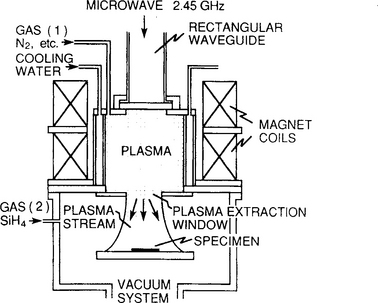
Figure 6-19 ECR plasma deposition reactor.
(From S. Matuso, in Handbook of Thin Film Deposition Processes and Techniques, ed. K. K. Schuegraf. Noyes, Park Ridge, NJ, 1988. Reprinted with permission from Noyes Publications.)
Other inductively coupled high-density plasma sources (helicon resonator), developed primarily for etching and briefly described in Section 5.4.5.4 have also been used for film deposition (Ref. 46). In general, the types and properties of films produced parallel those deposited in ECR reactors.
6.7.3 PECVD PROCESSES
6.7.3.1 Microelectronics Applications
In recent years the need for new materials coupled with lower processing-temperature requirements in different but related applications, e.g., ULSI (ultralarge-scale integrated) circuits, solar cells, and flat-panel displays, have made PECVD film deposition and plasma-etching methods indispensable. This is illustrated in a recent issue of the IBM Journal of Research and Development (Ref. 47) devoted to plasma processing. Among the involved materials are silicon-based semiconductors, insulators such as amorphous silicon and boron or phosphorus-doped SiO2, silicon nitride, and silicon oxynitride.
Plasma-processing methods of these materials can be best appreciated by reviewing a couple of cutting-edge applications in ULSI technology (Ref. 48). The first deals with the intermetal dielectric in logic integrated circuit chips. Previously (in Sections 5.4.2 and 5.3.4.3), methods of patterning and sputtering metal interconnections at various metallization levels were described. Here we comment on the intermetal SiO2 dielectric which must fill, without containing internal voids, the gaps between the interconnections. In this regard a comparison between different oxide deposition methods is instructive. Conventional PECVD dielectric films derived from a SiH4 source have a pronounced breadloaf appearance when deposited over an interconnect-stepped substrate. There is less breadloaf cusping (Fig. 6-20a) if TEOS is used because of the higher surface-mobility of the reactants. Nevertheless, a void still forms if the trench gap is too small because the oxide is not completely conformal, i.e., the deposit thickness is greater at the top than bottom of the trench. In contrast, conformal coverage is typical for ozone-TEOS deposition by thermal atmospheric as well as subatmospheric CVD (Fig. 6-20b). To eliminate breadloafing during gap filling by PECVD, some combination of sequential deposition and etching steps is required, e.g., PECVD-argon sputter etch-PECVD. But, if RF bias is applied to the substrate within high-density plasma reactors, significant ion bombardment and sputter etching occurs simultaneously with deposition. A triangular instead of breadloaf oxide structure (Fig. 6-20c) emerges that is more readily planarized by subsequent chemical–mechanical polishing.
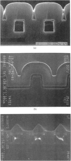
Figure 6-20 Scanning electron microscope cross-sectional images of oxide films grown by plasma and thermal CVD means. (a) TEOS-based PECVD; (b) TEOS-based atmospheric-pressure thermal CVD; (c) silane-based high-density plasma CVD.
(From Ref. 48. Copyright © 1999 by IBM Corp. Reprinted by permission.)
The deposition/sputter-rate ratio (D/S) is an important measure of the gap filling capability of this one-step process. Low D/S ratios facilitate filling of high-aspect-ratio trench structures, but if it is too low, corners of the features to be filled tend to be sputtered off (i.e., corner clipping). On the other hand, high D/S ratios lead to seams and voids. Typical deposition conditions for SiO2 gap filling of a 0.25- μ m wide, 0.62- μ m deep structure in a HDPCVD system include the following: RF power, 2 to 4 kW; gases, SiH4/Ar/O2; pressure, < 5 mtorr; D/S = 3.2/1; deposition temperature, 250–350°C; deposition rate, 100–400 nm/min.
A second set of PECVD applications in ULSI-DRAM cells for memory chips is schematically depicted in Fig. 6-21. Aside from the heart of the DRAM cell consisting of the interconnected field-effect transistor/deep-trench capacitor, the metal, oxide, glass and nitride films that are deposited parallel those for logic chips.

Figure 6-21 Schematic drawing of a three-level DRAM cell illustrating actual and potential (bold font) plasma CVD applications.
(From Ref. 48. Copyright © 1999 by IBM Corp. Reprinted with permission.)
6.7.3.2 Plasma Modification of Metal Surfaces
In the plasma nitriding and carburizing processes treated in this section, nitride and carbide films are not deposited. Instead, the atoms of nitrogen and carbon that deposit on metal surfaces modify them by diffusing into the underlying matrix. Except for the plasma assist and low pressures, these processes are very much like traditional nitriding and carburizing, which in essence are high-temperature, atmospheric-pressure CVD treatments. Plasma (or ion) nitriding of steels, one of the earliest commercial uses of plasmas, is generally accomplished in DC glow discharges generated at a potential difference of 300–1000 V between the workpiece cathode and the chamber walls (Ref. 44). Since the former may have complex three-dimensional shapes, it is important to conformally surround them with a “glow seam.” These workpieces are maintained below 600°C and subjected to N2/H2 mixtures at pressures between∼0.5 and 5 torr. Under these conditions a very hard nitrogen-rich layer some 2–10 μ m thick, consisting of assorted FexN (x = 2–4) compounds, forms within a diffusion zone a few hundred microns deep. By adding CH4 and CO2 to the gas mix, carbo-nitriding of surfaces can be achieved.
The process of plasma carburizing is carried out in an Ar/H2 atmosphere containing CH4 or C3H8 reactants at pressures between∼3 and 20 torr at temperatures of∼1000°C. Among the advantages claimed for such plasma treatment are enhanced mass transfer of carbon and prevention of surface and intergranular oxidation, a feature that confers greater resistance to mechanical fatigue damage. Despite this, plasma carburizing of steel has not displaced conventional heat-treating to the same extent that its low-temperature plasma-nitriding counterpart has. Plasma modification of other metals, e.g., nitriding of titanium alloys, and by different processes, e.g., plasma boriding of steel, are additional variations on the theme. By extrapolation to high-energy pulsed-plasmas, there is the PIII process discussed in Section 5.5.6. In common, these processes all rely on the undersized atoms of N, C, and B. These rapidly diffuse interstitially or can be readily implanted into metal matrices, and once incorporated they readily react to form generally hard metal nitride, carbide, and boride compounds.
It is not difficult to estimate the depth profiles in these processes. If there are negligible ion-implantation effects, ions simply impinge on the solid surface and diffuse in. We may assume the surface ion current-density (j) is essentially equivalent to a diffusion flux (J), i.e., J = j/q, where q is the charge per ion and J has units of ions/cm2-s. A boundary-value problem somewhat different from the two presented in Section 1.6.1, but like the one in Section 3.5.2.3, is then suggested. As before, we assume that there are no subsurface atoms (ions) initially, i.e., C(x, 0) = 0, and that C(x = 8, t) = 0. However, at the surface of our one-dimensional semiinfinite solid, D(dC/dx) (x = 0, t > 0) = j/q, where D is the effective diffusion coefficient.
Under these conditions the solution to Eq. 1-24 is
is linearly dependent on j. As C(x = 0) rises parabolically in time, the slope (dC(x)/dx) x= 0 remains invariant.
6.7.4 MODELING CHEMICAL REACTIONS IN PLASMAS
Since the complexity of plasmas is so great and our ability to treat chemical interactions in them so limited, computer simulation often offers the only salvation for predicting the kinetics of film deposition and etching processes in actual reactors. Much progress has been made in this regard starting from first principles as reviews (Refs. 49, 50) of this complicated subject indicate. It is therefore worth considering typical steps involved in modeling such plasma processes. One formulation conceptually breaks the overall simulation into three tasks: (1) the electron kinetics, (2) the plasma chemistry, and (3) the surface reactions, each with separate models.
1. The electron kinetics submodel assumes or calculates the electric (and magnetic) field and generates electron-impact cross sections and rate constants for use in the plasma-chemistry model. This phase involves modeling of sheath characteristics and calculation of electron densities that vary spatially and with time (for AC discharges), as a result of drift, diffusion, and assorted inelastic ionization, dissociation, attachment, etc., collisions. Values of ![]() for various electron–particle collisions are the goal and much progress has been made in this regard.
for various electron–particle collisions are the goal and much progress has been made in this regard.
2. The plasma-chemistry submodel provides a self-consistent accounting of the concentration of neutrals, radicals, and charged species as a function of space and time while conserving their mass, energy, and charge. Each reactant and product specie is treated separately and its motion due to diffusion, drift, and convective gas transport is folded together with information (from submodel 1) on collision-induced chemical reactions. Chemistries that have been modeled include those for hydrocarbon (e.g., CH4) and silane-based deposition systems as well as those for fluorocarbon (e.g., CF4), chlorine, and SF6-based etching processes.
3. The surface reaction submodel attempts to describe net sticking rates of gas-phase species, the kinetics of adsorption, and interaction of bombarding ions and radicals with the first few layers of the substrate. Objectives include an understanding of the physical and chemical mechanisms of film deposition and etching where a particular focus is anisotropic etching. In general, surface interactions are the least well understood of all plasma-related reactions.
Each of the submodels is intimately coupled to the other submodels. Thus the output of submodel 1 in the form of electron impact rates serves as the input for the mass conservation equations of the plasma-chemistry submodel. Similarly, computational feedforward as well as feedback paths exist between the plasma-chemistry and surface-reaction submodels. When possible, additional experimental data in the form of discharge breakdown fields, spectral information, and light output from added actinometer gases (whose optical emission-rate coefficients are known) assist the computational process.
Modeling of the type described above for SiO2 film deposition in high-density (microwave) plasma reactors has been reviewed by Meeks et al. (Ref. 51). Rate coefficients were calculated and tabulated for some 167 gas-phase reactions involving electron and particle collisions within simulated Ar, O2, and SiH4 plasmas. The results were reported in the form k = ATB exp–(C/T), where A, B, and C are constants. An additional 96 reaction-rate parameters were also tabulated for surface reactions in the same simulated plasmas. Comparisons of theoretically derived oxide growth rates with measured rates, as a function of substrate temperature and gas composition, are shown in Fig. 6-22.
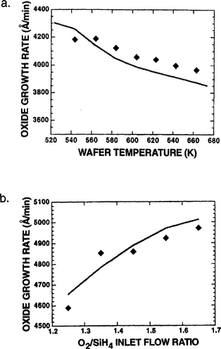
Figure 6-22 Comparison between experiment and theory in the growth of SiO2 in a high-density (microwave) plasma reactor. (a) Oxide growth rate vs temperature. —— model; ♦ data from D. R. Denison, LAM Research Corp. (b). Oxide growth vs O2/SiH4 flow ratio. —— model; ♦ data from C. Apblett, Sandia National Labs.
(From Ref. 51, Fig. 7. Reprinted with the permission of Dr. Ellen Meeks.)
6.8 SOME CVD MATERIALS ISSUES
6.8.1 INTRODUCTION
In this section we consider several unconventional CVD materials, explore their composition, microstructure, and properties, and discuss processes to deposit them. As specific examples we shall treat silicon and silicon-nitride films, present the extraordinary properties of diamond films and other ultrahard materials, and consider novel processes to selectively deposit films. Our discussion will naturally invite comparisons with competitive materials or processes, and further expose the diversity of CVD methods. Inasmuch as it is the key to understanding properties, a brief discussion of film structure is a good place to start.
6.8.2 STRUCTURE OF THERMAL CVD SILICON FILMS
Actual film and coating structural morphologies that develop are the result of complex nucleation and growth processes. Since the kinetic details are similar in all film formation and growth processes irrespective of whether deposition is chemical or physical in nature, they will be treated within a common framework in the next three chapters. Perhaps the two most important variables affecting growth morphologies are vapor supersaturation and substrate temperature. The former influences the film nucleation rate while the latter affects the growth rate. In concert they influence whether epitaxial films, platelets, whiskers, dendrites, coarse-grained polycrystals, fine-grained polycrystals, amorphous deposits, gas-phase powder, or some combination of these form. Thus, single-crystal film growth is favored by low gas supersaturation and high substrate temperatures, whereas amorphous film formation is promoted at the opposite extremes of high supersaturations and low temperatures.
An example of the way substrate temperature affects the structure of deposited Si films (Ref. 52) is shown in Fig. 6-23. Decomposition of silane at temperatures of about 600°C and below yields amorphous films with no detectable structure. Polysilicon films deposited from 600 to 650°C have a columnar structure with grain sizes ranging from 0.03 to 0.3 μ m, and possess a [110] preferred orientation. Larger Si crystallites form at higher temperatures, and eventually single-crystal or epitaxial film growth can be achieved at 1200°C.
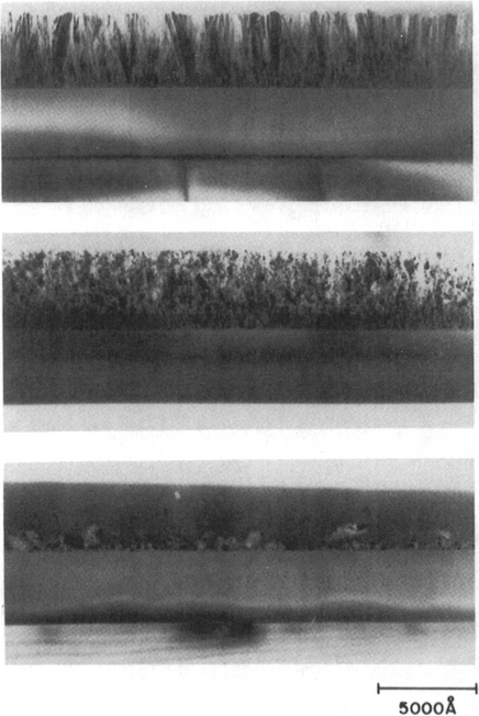
Figure 6-23 Morphology of poly-Si deposited from SiH4 on an SiO2 substrate. (Top) Columnar grains deposited above 650°C. (Middle) Fine-grained poly-Si. (Bottom) Partly amorphous structure deposited at 625°C. Deposition at temperatures below 600°C produces structureless amorphous films.
(From Ref. 52. Courtesy of R. B. Marcus, reprinted with permission from John Wiley & Sons.)
6.8.3 DEPOSITION AND STRUCTURE OF AMORPHOUS SILICON FILMS
Amorphous silicon (a-Si) and hydrogenated versions of it, e.g., a-Si:H, are the basic materials discussed in this section. They have been deposited by both PVD and CVD techniques. Of the elements, silicon and others in column IV of the periodic table are among the easiest to prepare in amorphous form. Further, they do not require particularly low substrate temperatures (Ts) for their preparation. When normalized to the melting point (Tm), the ratio of TS/TM for amorphous CVD materials is higher by at least a factor of∼5 relative to what is required to amorphize typical PVD metal alloys. What accounts for the particular ease in amorphizing Si by CVD is the steric hindrance provided by molecular groups. Such structural obstruction leads to the high viscosity conducive to glass formation in bulk hydrocarbon polymers and oxide melts. In the case of a-Si:H films derived from SiH4–H2 mixtures, for example, the assorted radical and molecular fragments, e.g., SiH3, SiH2, Si2H6, are the source of the steric hindrance. A continuum of Si–H structures links the gas phase of SiH4 + H2 to the deposit surface. Contained within this transition region are assorted fragmented molecular species, which in turn connect to the film growth zone and eventually to the stable a-Si:H network beneath the film surface. Atom incorporation reactions are complex and not known with certainty (Refs. 53, 54); they resemble network polymerization of assorted SinH2n molecular fragments and include dissociation and hydrogen desorption as well. The net result is the incorporation of as much as 35 at.% hydrogen (Ref. 55) into a silicon deposit disordered by bond stretching and distortion.
6.8.4 AMORPHOUS SILICON NITRIDE
Silicon nitride is normally prepared by reacting silane with ammonia in an argon plasma, but a N2/SiH4 discharge can also be used. During plasma deposition, as much as 30 at.% hydrogen can be incorporated which apparently forms bonds to both Si and N. It is in this sense that silicon nitride is often described as a ternary solid-solution alloy, SiNH. Amorphous silicon nitride should be distinguished from the stoichiometric compound, Si3N4, formed by reacting silane and ammonia at 900°C in an atmospheric CVD reactor. It is instructive to further compare the physical and chemical property differences in three types of silicon nitride (Refs. 56, 57), and this is done in Table 6-5. While Si3N4 is denser and more resistant to chemical attack and has higher resistivity and dielectric breakdown strength, SiNH tends to provide better step coverage. An upper temperature limit that can be tolerated in some completed integrated circuits is∼300°C because interconnection metallizations begin to react with the surrounding insulation beyond this point. Since SiHN can be deposited at such temperatures and is an effective barrier against moisture penetration, it has been used to encapsulate IC chips.

Further aspects of the structure of amorphous elemental and alloy films, including silicon nitride, will be deferred to Section 9.6.
6.8.5 ULTRAHARD THIN FILMS
In this section we discuss films based on the three hardest substances known, diamond, boron nitride, and carbon nitride, and consider their deposition, properties, and uses. In common, they are all primarily produced by CVD methods. Diamond is by far the most important of these materials and is therefore given the greatest attention.
6.8.5.1 Introduction to Diamond and Carbons
Derived from the Greek αδαμασ (adamas), which means unconquerable, diamond is the most extraordinary of materials. Diamond is indeed an invincible material. In addition to being the most costly on a unit weight basis, and capable of unmatched beauty when polished, diamond has a number of other remarkable properties. It is the hardest substance known (Hk > 8000 kg/mm2) and has a higher modulus of elasticity (1050 GPa) than any other material. When free of impurities, it has one of the highest electrical resistivities (∼ 1016 Ω -cm). It also combines a very high thermal conductivity (2000 W/m-K), which is some 4 to 5 times that of Cu and Ag, with a low thermal expansion coefficient (1.2 × 10⁻⁶K−1) to yield a high resistance to thermal shock. Other less extraordinary but nevertheless interesting properties include resistance to chemical attack, high breakdown voltage, large bandgap energy, and transparency to visible, infrared, and microwave radiation. Diamond’s remarkable attributes, the first three in particular, spurred one of the most exciting and competitive quests in the history of materials science–the synthesis of bulk diamond. Success was achieved with the 1954 GE Corp. process utilizing extremely high pressures and temperatures in the diamond-stable region of the carbon phase diagram (Fig. 1-12).
Isolated C atoms have distinct 2s and 2p atomic orbitals. When these atoms condense to form diamond, electronic admixtures occur resulting in four equal hybridized sp3 molecular orbitals. Each C atom is covalently attached to four other atoms in tetragonal bonds 1.54 Å long, creating the well-known diamond cubic structure (Fig. 1-2c). Graphite, on the other hand, has a layered structure. The C atoms are arranged hexagonally with strong trigonal bonds (sp2) and have an interatomic spacing of 1.42 Å in the basal plane. A fourth electron in the outer shell forms weak van der Waals bonds between planes which account for such properties as good electrical conductivity, lubricity, lower density, softness, and a grayish-black color.
In addition, C exists in a variety of metastable and amorphous forms which have been characterized as degenerate or imperfect graphitic structures. Here layer planes are disoriented with respect to the common axis and overlap each other irregularly. Beyond the short-range graphitic structure, the matrix consists of amorphous C. A complex picture now emerges of the manifestations of C ranging from amorphous to crystalline forms in a continuum of structural admixtures. Similarly, the proportions of sp2 –sp3 (and even sp1) bonding are variable, causing the different forms to have dramatically different properties. Not surprisingly, this broad spectrum of metastable carbons have been realized in thin-film deposits. What now complicates matters further is that the many techniques to produce carbon films use hydrocarbon gases. Hydrogen is, therefore, inevitably incorporated, and this adds to the complexity of the deposit structure, morphology, and properties. Given the structural and chemical diversity of carbon films, an understandable confusion has arisen with regard to the description of these materials. Labels such as hard carbon, amorphous carbon (a-C), hydrogenated amorphous carbon (a-C:H), and diamond-like carbon (DLC), as well as diamond, have all been used in the literature. The ensuing discussion will treat the deposition processes and properties of these films with the hope of clarifying some of their distinguishing features.
6.8.5.2 Film Deposition Processes
Attempts to produce diamond from low-pressure vapors date back at least to 1911 (Ref. 58), and by the mid 1970s Derjaguin and Fedeseev (Ref. 59) had apparently grown epitaxial diamond films and whiskers during the pyrolysis of various hydrocarbon–hydrogen gas mixtures. After a decade of relative quiet, an explosive worldwide interest in the synthesis of diamond films and their properties erupted which persists to the present day.
6.8.5.2.1 Diamond
Thin diamond films involve metastable synthesis in the low-pressure graphite region of the phase diagram. The possibility of synthesizing diamond in this region is based on the small free-energy difference, i.e., 500 cal/mol, between diamond and graphite under ambient conditions (Ref. 60). Therefore, a finite probability exists that both phases can nucleate and grow simultaneously, especially under conditions where kinetic factors dominate, i.e., high energy or supersaturation. In particular, the key is to prevent graphite from forming or to remove it preferentially, leaving diamond behind. The way this is done practically is to generate a supersaturation or superequilibrium of atomic H. The latter has been most commonly produced utilizing 0.2–2% CH4–H2 mixtures in DC, RF, and microwave plasmas, or in thermal CVD reactors containing hot filaments. Under these conditions the atomic H that is generated fosters diamond growth by inhibiting graphite formation, by dissolving it if it does form, by stabilizing sp3 bonding, or by promoting some combination of these factors. In general, hydrocarbon, e.g., CH4, C2H2, decomposition at substrate temperatures of 800–900°C in the presence of atomic H is conducive to diamond growth on nondiamond substrates. Paradoxically, the copious amounts of atomic H result in very little hydrogen incorporation in the deposit. The beautiful SEM images (Fig. 6-24) of small faceted diamond crystallites produced in the manner just described have captured the imagination of the world.

Figure 6-24 Diamond crystals grown by CVD employing combined microwave and heated filament methods.
(Courtesy of T. R. Anthony, GE Corporate Research and Development.)
In retrospect, low-pressure diamond synthesis has proven to be not nearly as prohibitively difficult as originally imagined. For example, diamond deposits readily at rates of∼15 μ m/h on abraded molybdenum substrates heated by the feather portion of an oxyacetylene torch flame (Ref. 61). High-quality crystals (>10 μ m in size) have been produced at 500–750°C with an O2/C2H2 ratio of 0.85–0.98.
An important consideration in commercial deposition processes employing cathodic arcs or CVD methods is the growth rate, which typically ranges up to 1000 μ m/h (1 mm/h). This should be compared to even higher rates for commercial production of diamond abrasive grain.
6.8.5.2.2 Diamondlike Carbon
Amorphous carbons containing hydrogen, are identified as a-C:H materials and possess diamondlike properties. Films are formed when hydrocarbons impact relatively low-temperature substrates with energies in the range of a few hundred eV. Plasma CVD techniques employing RF and DC glow discharges in assorted hydrocarbon gas mixtures commonly produce a-C:H deposits (Ref. 62). Substrate temperatures below 300°C are required to prevent graphitization and film softening. The energetic molecular ions disintegrate upon hitting the surface and this explains why the resulting film properties are insensitive to the particular hydrocarbon employed. It is thought that the incident ions undergo rapid neutralization and the carbon atoms are inserted into C–H bonds to form acetylenic and olefinic polymerlike structures, e.g., C + R–CH3 → R–CH = CH2, where R is the remainder of the hydrocarbon chain. The resultant diamondlike films, therefore, contain variable amounts of hydrogen with H/C ratios ranging anywhere from∼0.2 to∼0.8 or more. Containing an admixture of sp3, sp2, and sp1 bonding, they may be thought of as glassy hydrocarbon ceramics and can be even harder than SiC.
6.8.5.2.3 Amorphous Carbon (a–C)
These diamond-like films are prepared at low temperatures in the absence of hydrocarbons by ion-beam-assisted or sputter-deposition techniques. Both essentially involve deposition of carbon under the bombardment of energetic ions. Simple thermal evaporation of carbon will, however, yield highly conductive, soft films whose properties are far removed from the hard, very resistive, high-energy bandgap diamond-like materials. Ion impact energy, therefore, appears to be critical in establishing the structure of the deposit. More diamond-like properties are produced at lower energies; microcrystalline diamond ceases to form when the ion energy exceeds∼100 eV, in which case the amorphous structure prevails.
6.8.5.3 Properties and Applications
The properties of CVD synthesized diamond, a-C, and a-C:H film materials (Refs. 60, 63) are compared with those of bulk diamond and graphite in Table 6-6. Basic differences in structure and properties of diamond and diamond-like films ultimately stem from the sp3/sp2 bond concentration ratios. Considerable bond admixtures occur in both the a-C:H and a–C films and much experimental effort has been expended in determining bonding proportions. Techniques such as Raman spectroscopy, nuclear magnetic resonance, and X-ray photoelectron spectroscopy (XPS) are used to characterize films and bolster claims for the presence of the elusive diamond crystals. Although there is a great deal of scatter in many of the film properties due to differing deposition conditions, it is clear that the films are extremely hard, chemically inert, and highly insulating.
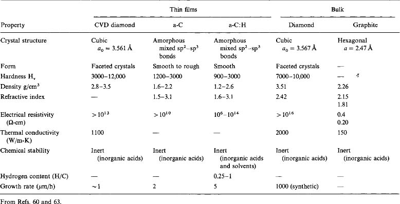
Diamond and diamond-like film materials are already commercially exploited in a number of technologies. For example: high thermal conductivity is the reason that diamond substrates are used for semiconductor-laser and microwave-device heatsinks; the ultrahardness of diamond coatings is exploited in extending the life of cutting tools and surfaces that wear; diamond’s extreme stiffness has been used on resonator diaphragms of tweeter loudspeakers to extend the frequency response to 60 kHz. For many applications crystalline diamond is not essential. Thus, DLC films are employed to protect magnetic information storage media. When such disks are started or stopped, the sliding contact that occurs beween the disk and slider can cause mechanical damage. To minimizae this while retaining high recording density, ultrasmooth DLC films less than 50 nm thick are used to coat hard disks and magnetic heads.
6.8.5.4 Boron Nitride and Carbon Nitride
Bulk cubic boron nitride (c-BN) is also a remarkable material. It has a hardness (70 GPa) second only to that of diamond (100 GPa), and its thermal conductivity, at half the diamond value, is still very high. However, diamond tools oxidize at low temperatures and cannot be used to machine Fe, Co, and Ni because of carbide formation. But c-BN is resistant to oxidation and is widely used to machine cast irons and steels. As with diamond-film synthesis, it is critical to form sp3-hybridized c-BN during deposition to attain superior properties. Thermal CVD methods below 1250°C, using B2H6, BF3, and B3N3H6 to provide the boron and N2 and NH3 the nitrogen, solely produce the noncubic, sp2-hybridized version of boron nitride that is amorphous or poorly crystallized. The hot-filament CVD so widely used to make diamond films does not appear to be successful for c-BN deposition. Plasma-assisted CVD methods for depositing c-BN have been reviewed by Konyashin et al. (Ref. 64). Typically, the same gases have been reacted together in a variety of RF, DC, ECR, laser enhanced, microwave, pulsed plasma, and inductively coupled plasma CVD reactors.
To explain the often contradictory effects of deposition variables on c-BN content in the films, these authors distinguish between physical and chemical routes taken in plasma CVD processes. The physical route generally means high-energy bombardment of biased substrates by Ar+ and N+ ions. Compressively stressed amorphous and hexagonal-BN layers deposit that are poorly adherent. Such structures are also seen during physical vapor deposition of BN films, where higher c-BN contents, albeit with an sp2-hybridized BN interlayer, generally deposit. In the chemical route, films deposit in much the same was as diamond, i.e., a hydrogen-rich plasma with high concentrations of atomic hydrogen. The latter etches away the sp2 bonds and converts them to sp3 bonds, enabling c-BN crystals to grow directly from the seeded substrate. Schematically depicted in Fig. 6-25 is a model for this reaction as well as the distinction between the two routes. Relative to bulk c-BN, the properties of deposited boron nitride films have clearly not advanced to the state enjoyed by diamond films relative to bulk diamond.

Figure 6-25 Illustration of physical (left) and chemical (right) routes in the production of boron nitride films. In the physical route Ar and N ion bombardment of a negatively biased substrate is emphasized, whereas PECVD in a hydrogen plasma is featured in the chemical route. Note the difference in c-BN growth morphology in each case.
(From Ref. 64. Reprinted with the permission of Professor F. Aldinger.)
Deposition of carbon nitride films has many of the earmarks of the earlier quest for the synthesis of diamond films. The excitement began when Liu and Cohen (Ref. 65) theoretically predicted that the bulk modulus of the hypothetical compound -C3N4, which is structurally similar to -Si3N4, should be 427 GPa; this compares with 440 GPa for diamond. Further, they suggested this phase, like diamond, has a high atomic density coupled with short strong bonds and could be metastable under ambient conditions. Badding (Ref. 66) has claimed that there is no convincing evidence for the successful synthesis of either crystalline or amorphous carbon nitrides containing primarily sp3-bonded carbon. Nevertheless, a hardness of 6500 kg/mm2 (64 GPa) has been reported in films physically deposited by ion-beam assisted methods (Ref. 67). Although PVD methods have been primarily used to deposit assorted carbon nitrides, CVD processes to do this have also been reported (Ref. 67).
6.8.6 SELECTIVE DEPOSITION OF FILMS
Of all the attractive features of CVD, perhaps none is as intriguing as the ability to selectively deposit thin films in desired regions and nowhere else. Although CVD is usually thought of as a large-area or blanket deposition technique, there are ways of promoting deposition on selected areas. Different techniques and mechanisms are involved depending whether the substrate is unpatterned or patterned. Selectivity on unpatterned or broad-area substrates by means of lasers has already been discussed in Section 6.6.5.
It is a much greater challenge to selectively deposit films on a patterned rather than blanket substrate. The former is the case in microelectronics where the geometric complexity and tiny dimensions involved preclude beam writing. Instead, selectivity is based on differences in interfacial chemical reactions taking place on different materials (Refs. 68, 69). Ideally, film nucleation must be respectively simultaneously stimulated and inhibited on the desired and undesired surfaces. An outstanding example of CVD selective growth is shown in Fig. 6-26, where tungsten is seen to deposit on exposed Si and not on the neighboring SiO2. Although tungsten can be deposited by thermal dissociation of WF6, reduction by hydrogen makes it possible to produce W films at a lower temperature of 300°C according to the chemical reaction of Eq. 6-4. But deposition of W occurs indiscriminately on all surfaces because the source (WF6) and reducing agent (H2) are gases. However, if the reducing agent is a solid, e.g., patterned elemental Si, then reaction occurs selectively on the exposed Si according to the reaction
Figure 6-26 Scanning electron micrograph of an array of tungsten crosses and meandering lines selectively deposited over silicon through reduction of WF6. Between the deposited tungsten is the uncoated SiO2 substrate.
(Courtesy of K. P. Rodbell, IBM, T. J. Watson Research Center.)
The Si in neighboring SiO2 cannot act as a reducing agent because it is already fully oxidized. As long as it is exposed to WF6, elemental Si continues to be sacrificed and selective growth proceeds. But after a while a thin film of W will fully cover the Si and the reaction ceases; growth is thus self-limiting. To grow thicker W films an excess concentration of H2 gas must be now added to reduce a diluted WF6 source gas. This results in a low supersaturation of W in the gas phase, which makes deposition on the previous selectively deposited tungsten more likely. Higher W supersaturation levels would more likely cause nucleation and growth everywhere including SiO2, thus destroying selectivity in the process.
A similar mechanism for selectivity is predicted to be operative for deposition of W on Al, Ti, TiSi2, and CrSi2 simply based on thermodynamic considerations; these substrates yield driving forces for WF6 reduction as high as that for Si (Ref. 68). For example, with a concentration ratio of H2/WF6 = 40, at a total pressure of 0.75 torr, the free energies for reactions with the above four metals (e.g., WF6+Al → W+AlF3) are, respectively, – 27.7, –17.2, –18.5, and –17.8 kJ/mol at 500 K. These values compare with – 18.4 kJ/mol for Si. The review by Hampden-Smith and Kodas (Ref. 41) lists mechanisms for selective deposition of metal films and the metals that are amenable to such processes; for example, volatile transition-metal organic-precursors (e.g., containing Cu) can selectively deposit on specific metals (e.g., Pt) relative to the nongrowth SiO2 surface, in a replacement type reaction.
In Section 8.7.3 we shall continue the discussion of selective deposition as it applies to epitaxial films.
6.9 SAFETY
The safe handling of gases employed in CVD systems is a concern of paramount importance. Safety is part of the larger concern for chemical hazards in the semiconductor industry. This subject has been reviewed (Ref. 70) with respect to risk assessment, redundant control technology, hardware issues, and government regulation. In the case of CVD reactant or product gases we are typically dealing with toxic, flammable, pyrophoric, or corrosive substances. Because they frequently possess a combination of these attributes, they present particular health hazards to humans. Exposure of reactor hardware and associated gas-handling equipment to corrosive environments also causes significant maintenance problems and losses due to downtime. Table 6-7 contains a list of gases commonly employed in CVD processes together with some of their characteristics. A simple entry in the table does not accurately reflect the nature of the gas in practice. Silane, for example, more so than other gases employed in the semiconductor industry, has an ominous and unpredictable nature. It is stable but pyrophoric so that it ignites on contact with air. If it accumulates in a stagnant air space, however, the resulting mixture may explode upon ignition. In simulation tests of leaks, high flow rates of silane have resulted in violent explosions. For this reason, silane cylinders are stored outside buildings in concrete bunkers. The safety problems are magnified in low-pressure processing where concentrated gases are used. For example, in the deposition of polysilicon pure silane is used during LPCVD, whereas only a few percent silane is employed in atmospheric-pressure CVD processing. Often cited for their safety, many MOCVD precursors are pyrophoric.
Table 6-7 Table 6-7 Hazardous Gases Employed in CVD

Corrosive attack of gas-handling equipment (e.g., valves, regulators, piping) occurs in virtually all CVD systems. The problems are particularly acute in LPCVD processing because of the damage to mechanical pumping systems. Since many reactors operate at high temperatures, the effluent gases are very hot and capable of further downstream reactions in the pumping hardware. Furthermore, the exhaust stream generally contains corrosive species such as acids, oxidizers, and unreacted halogenated gases, in addition to large quantities of abrasive particulates. In semiconductor processing, for example, silica and silicon nitride particles are most common. All of these products are ingested by the mechanical pumps and the chamber walls become coated with precipitates or particulate crusts. Oils used are degraded through polymerization and incorporation of solids. This hampers the lubrication of moving parts and hardware, and they tend to corrode and wear out more readily. All of this is a small price to pay, however, for the wonderful array of film materials that CVD has made possible.
6.10 CONCLUSION
Instead of the physical transfer of atoms from a condensed evaporation source or sputtering target to the substrate, chemical vapor deposition primarily relies on gas phase and gas–solid chemical reactions to produce thin films. Because they are subject to thermodynamic and kinetic limitations and constrained by the flow of gaseous reactants and products, CVD processes are generally more complex than those involving PVD. However, guidelines adopted from the disciplines of physical chemistry, heat and mass transport, and fluid dynamics have provided a useful basis for analyzing and modeling these processes. Just as there are liquid and solid solutions, we may think of chemically reactive gas solutions in CVD, where an insoluble solid thin film can be made to controllably precipitate on a substrate under suitable temperatures and pressures. This chapter has been concerned with the strategies used to ensure that this gas-phase precipitation occurs at appreciable rates, to yield amorphous, polycrystalline, and epitaxial films with desired film compositions, morphologies, and structures.
An impressive number of different CVD materials (metals, elemental and compound semiconductors, oxides, nitrides, carbides, diamond, etc.) are of scientific and technical interest for a variety of electronically, optically, mechanically, and environmentally functional purposes. These materials and applications needs have been fulfilled through a variety of CVD processes involving different reactor designs and operating conditions. On the one hand there are thermal CVD processes that are conducted at both high and low temperatures, maintained at atmospheric as well as reduced pressures. Alternatively there are low-pressure, plasma-enhanced CVD processes that have been developed to deposit films at lower temperatures and on thermally sensitive substrates. In both categories the number of suitable gaseous precursors for CVD processes has been expanded through the synthesis of volatile metalorganic compounds. Developed particularly for the deposition of epitaxial semiconductor films, MOCVD processes are now increasingly used for the deposition of multicomponent oxide films as well. Included among the many desirable features of CVD processes is the unique capability of selective deposition.
In concluding this chapter our discussion of film deposition processes has ended for the moment. However, we shall return to other CVD processes in Chapter 8 and consider the demanding application of the epitaxial deposition of compound semiconductors.
1. Consider the generic reversible CVD reaction
at 1 atm pressure (PA + Pc = 1), where the free energy of the reaction is ΔG° = ΔH° – TΔS°. Through consideration of the equilibria at T1 and T2:
2. It is desired to deposit epitaxial silicon films from a SiHCl3 precursor gas in an atmospheric pressure CVD reactor.
3. Plot ln ![]() vs 1/TK for the temperature range 800 to 1500 K, using the results of Fig. 6-6.
vs 1/TK for the temperature range 800 to 1500 K, using the results of Fig. 6-6.
4. In growing epitaxial Ge films by the disproportionation reaction of Eq. 6-14, the following thermodynamic data apply:

5. Assume you are involved in a project to deposit ZnS and CdS films for infrared optical coatings. Thermodynamic data reveal
6. The disproportionation reaction Si + SiCl4 = 2SiCl2 (ΔG° = 83,000+ 3.64T log T–89.4T (cal/mol)) is carried out in a closed tubular atmospheric pressure reactor whose diameter is 15 cm. Deposition of Si occurs on a substrate maintained at 750°C and located 25 cm away from the source, which is heated to 900°C. Assuming thermodynamic equilibrium prevails at source and substrate, calculate the flux of SiCl2 transported to the substrate if the gas viscosity is 0.08 cP.
7. Consider the deposition of silicon carbide utilizing two independent source gases CH4 and SiCl4 according to Eq. 6-9. According to the Gibbs phase rule, what thermodynamic variables and compositions would have to be specified before the system is determinate?
9. Polysilicon deposits at a rate of 30 Å/min at 540°C. What deposition rate can be expected at 625°C if the activation energy for film deposition is 1.65 eV?
10. Tetrachlorosilane diluted to 0.5 mol% in H2 gas flows through a 12-cm-diameter, tubular, atmospheric CVD reactor at a velocity of 20 cm/s. Within the reactor is a flat pallet bearing Si wafers resting horizontally. If the viscosity of the gas is 0.03 cP at 1200°C:
11. Find the stoichiometric formula for the following films:
12. Consider a long tubular CVD reactor in which one-dimensional steady-state diffusion and convection processes occur together with a homogeneous first-order chemical reaction. Assume the concentration C(x) of a given species satisfies the ordinary differential equation
where k is the chemical rate constant and x is the distance along the reactor.
13. An ion nitriding system operates at a nitrogen pressure of 1 torr. Nitriding was done at 500°C, and the diffusivity of N in steel is given by
After a 3-h exposure of a tool steel to the discharge, the nitrogen content rose from zero to 0.5% at a distance 10 μ m beneath its surface.
14. Select any film material (e.g., semiconductor, oxide, nitride, carbide, metal alloy) that has been deposited or grown by both PVD and CVD methods. In a report, compare the resultant structure, stoichiometries, and properties. The Journal of Vacuum Science and Technology and Thin Solid Films are good references for such information.
15. As manager of a coating facility with complete PVD and CVD capabilities, recommend the tooling and procedures necessary to coat the following items:
16. A gas mixture flows along a tubular reactor of cross-sectional area A with velocity v. Downstream along the x direction, a first-order chemical reaction with rate constant k occurs on substrates of area As, thus continuously depleting the gas.
17. List several ways to suppress unstable gas flows that adversely affect films deposited in CVD reactors.
1 Sherwood E.M., Blocher J.M. J. Metals. 1965;17:594.
2 Sivaram S. Chemical Vapor Deposition—Thermal and Plasma Deposition of Electronic Materials. New York: Van Nostrand Reinhold; 1995.
3 Hampden-Smith M.J., Kodas T.T. The Chemistry of Metal CVD. Weinheim: VCH, 1994.
4 Hitchman M.L., Jensen K.F. Chemical Vapor Deposition, Principles and Applications. London: Academic Press, 1993.
5 Pierson H.O. Handbook of Chemical Vapor Deposition, Principles, Technology and Applications. Park Ridge, NJ: Noyes, 1992.
6 Sherman A. Chemical Vapor Deposition for Microelectronics. Park Ridge, NJ: Noyes; 1987.
7 . Several review articles are devoted to plasma processing. IBM J. Res. Develop.. 1999;43. 1/2
8 Vossen J.L., Kern W. Several review articles on thermal and plasma-assisted CVD appear. Thin Film Processes. New York: Academic Press; 1991;II.
9 Kern W. Levy R.A., editor. Microelectronic Materials and Processes. Dordrecht, The Netherlands: Kluwer Academic, 1989.
10 Kern W., Ban V.S. Vossen J.L., Kern W. Thin Film Processes. New York: Academic Press, 1978.
11 Schlichting J. Powder Metal Int.. 1980;12(3):141.
12 Wajda E.S., Kippenhan B.W., White W.H. IBM J. Res. Develop.. 1960;7:288.
13 Laudise R.A. The Growth of Single Crystals. Englewood Cliffs, NJ: Prentice Hall; 1970.
14 Sirtl E., Hunt I.P., Sawyer D.H. J. Electrochem. Soc.. 1974;121:919.
15 Ban V.S., Gilbert S.L. J. Electrochem. Soc.. 1975;122(10):1382.
16 Hay S.O., Roman W.C., Colket M.B. J. Mater. Res.. 1990;5:2387.
17 Anthony T.C., Fahrenbruch A.L., Bube R.H. J. Vac. Sci. Technol.. 1984;A2(3):1296.
18 Perrier G., Philippe R. J. Mater. Res.. 1988;3(5):1031.
19 Nishino S., Matsumoto K., Yoshida T., Chen Y., Lilov S.K. Mat. Sci. Eng.. 1999;B61-62:121.
20 Lee H.H. Fundamentals of Microelectronics Processing. New York: McGraw-Hill; 1990.
21 Middleman S., Hochberg A.K. Process Engineering Analysis in Semiconductor Device Fabrication. New York: McGraw-Hill; 1993.
22 Jensen K.F., Kern W. Vossen J.L., Kern W., editors. Thin Film Process, II. Boston: Academic Press, 1991.
23 Kleijn C. Transport Phenomena in Chemical Vapor Deposition Reactors. Ph.D. thesis. The Netherlands: Technical University of Delft; 1991.
24 Rundle P.C. Int. J. Electron.. 1968;24:405.
25 Hitchman M.L., Jensen K.F. Hitchman M.L., Jensen K.F. Chemical Vapor Deposition, Principles and Applications. London: Academic Press, 1993.
26 Grove A.S. Physics and Technology of Semiconductor Devices. New York: John Wiley & Sons; 1967.
27 Ruska W.S. Microelectronic Processing. New York: McGraw-Hill; 1987.
28 Rickerby D.S., Matthews A. Advanced Surface Coatings. Glasgow: Blackie (Chapman and Hall), 1991.
29 Li J., McVittie J.P., Ferziger J., Saraswat K.C. J. Vac. Sci. Technol.. 1995;B13:1867.
30 Lassig S.E., Tucker J.D. Microelectron. J.. 1995;26(8):xi.
31 Nag S., Ramamurthy R., Lei W.J., Montell C., Hickey M. Solid State Technol.. 1998;41(9):69.
32 Manasevit H.M., Simpson W.I. Appl. Phys. Lett.. 1975;12:172.
33 Wessels B.W. Ann. Rev. Mater. Sci.. 1995;23:525.
34 Palkar V.R., Purandare S.C., Pinto R. J. Phys. D: Phys.. 1999;32:Rl.
35 Kotecki D.E., et al. IBM J. Res. Develop.. 1999;43(3):367.
36 Jones A.C. Chem. Vap. Deposition. 1998;4(5):169.
37 Braunstein G., Paz-Pujalt G.R. Thin Solid Films. 1992;1(216).
38 Tuttle B.A., Schwartz R.W. MRS Bull.. 1996;21(6):49.
39 Baum T.H., Comita P.B. Thin Solid Films. 1992;218:84.
40 Hampden-Smith M.J., Kodas T.T. Chem. Vap. Deposition. 1995;1:8.
41 Hampden-Smith M.J., Kodas T.T. Chem. Vap. Deposition. 1995;1:39.
42 McCrary V.R., Donnelly V.M. Hitchman M.L., Jensen K.F. Chemical Vapor Deposition, Principles and Applications. San Diego: Academic Press, 1993.
43 Veprek S. Thin Solid Films. 1985;130:135.
44 Rie K.-T., Menthe E., Matthews A., Legg K., Chin J. MRS Bull.. 1996;21(8):46.
45 Lucovsky G., Tsu D.V., Rudder R.A., Markunas R.J. Vossen J.L., Kern W., editors. Thin Film Processes, II. New York: Academic Press, 1991.
46 Nguyen S.V. IBM J. Res. Develop.. 1999;43(1/2):109.
47 Kuo Y., editor. IBM J. Res. Develop. 1999;43. 1/2
48 Cote D.R., Nguyen S.V., Stamper A.K., Armbrust D.S., Tobben D., Conti R.A., Lee G.Y. IBM J. Res. Develop.. 1999;43(1/2):5.
49 Klein L.E., Kushner M.J. Crit. Rev. Solid State Mater. Sci.. 1989;16:1.
50 Hamaguchi S. IBM J. Res. Develop.. 1999;43(1/2):199.
51 Meeks E., Larson R.S., Ho P., Apblett C., Han S.M., Edelberg E., Aydil E.S. J. Vac. Sci. Technol.. 1998;A16(2):544.
52 Marcus R.B., Sheng T.T. Transmission Electron Microscopy of Silicon VLSI Circuits and Structures. New York: John Wiley & Sons; 1983.
53 Smith D.L. Thin-Film Deposition. New York: McGraw-Hill; 1995.
54 Perrin J. Williams P.F., editor. Plasma Processing of Semiconductors. The Netherlands: Kluwer, Dordrecht, 1997.
55 Hess D.W., Graves D.B. Hitchman M.L., Jensen K.F. Chemical Vapor Deposition, Principles and Applications. San Diego: Academic Press, 1993.
56 Adams A.C. Sze S.M., editor. VLSI Technology. New York: McGraw-Hill, 1988.
57 Hollahan J.R., Rosier S.R. Vossen J.L., Kern W. Thin Film Processes. New York: Academic Press, 1978.
58 von Bolton W. Z. Electrochem.. 1911;17:971.
59 Bridgeman P.D. Sci. Am.. 1975;233:102.
60 DeVries R.C. Ann. Rev. Mater. Sci.. 1987;7:161.
61 Ravi K.V., Koch C.A., Hu H.S., Joshi A. J. Mater. Res.. 1990;5:2356.
62 Grill A. IBM J. Res. Develop.. 1999;43:147.
63 Tsai H.C., Bogy D.B. J. Vac. Sci. Technol.. 1987;A5:3287.
64 Konyashin I., Bill J., Aldinger F. Chem. Vap. Deposition. 1997;3(5):239.
65 Liu A.Y., Cohen M.L. Science. 1989;245:841.
66 Badding J.V. Adv. Mater.. 1997;9(11):877.
67 Inoue T., Ohshio S., Saitoh H., Kamata K. Appl. Phys. Lett.. 1995;67:353.
68 Carlsson J.-O. Crit. Rev. Solid State Mater. Sci.. 1990;16(3):161.
69 Carlsson J-O., Jansson U. Prog. Solid State Chem.. 1993;22:237.
70 Chelton C.F., Glowatz M., Masovsky J.A. IEEE Trans. Education. 1991;34(3):269.