
Chapter 7 Substrate Surfaces and Thin-Film Nucleation
7.1 INTRODUCTION
In keeping with the theme and subtitle, the preceding half of the book was broadly devoted to the deposition of thin films. This chapter is the first of three that directly deal with the multifaceted concerns of the second theme–film structure. These three chapters encompass the progression of events that starts with the condensation of isolated atomic clusters on a bare substrate, continues with film thickening due to additional deposition, and ends with fully developed epitaxial single-crystal, polycrystalline, or amorphous films and coatings. Included will be issues related to the physical and crystallographic nature of substrates, film–substrate interfacial interactions, and the evolution of the film grain structure and morphology. The overall objective of these three chapters is to reconcile film structure with prior processing on the one hand, and serve as a springboard for understanding film properties on the other. In this sense these chapters are the filling sandwiched between prior and subsequent chapters.
Interest in thin-film formation dates at least to the 1920s. In the course of research at the Cavendish Laboratories in England on evaporated thin films, the concept of formation of nuclei which grew and coalesced to form the film was advanced (Ref. 1). During the earliest stages of film formation a sufficient number of vapor atoms or molecules condense and establish a permanent residence on the substrate. Many such film birth events occur in this so-called nucleation stage. Numerous investigations employing assorted techniques, e.g., transmission and scanning electron microscopy, Auger-electron spectroscopy, and now scanning probe microscopies, have focused on the earliest stages of film formation. These studies typically reveal that the demarcation between the end of nucleation and the onset of nucleus growth is not sharp. The sequence of film nucleation and growth events can be well appreciated in the transmission-electron microscopy images of Fig. 7-1. Soon after exposure of the substrate to the incident vapor, a uniform distribution of small but highly mobile clusters or islands is observed. In this stage the prior nuclei incorporate impinging atoms and subcritical clusters and grow in size while the island density rapidly saturates. The next stage involves merging of the islands by a coalescence phenomenon which, in some cases, is liquid-like, especially at high substrate temperatures. Coalescence decreases the island density resulting in local denuding of the substrate where further nucleation can then occur. Crystallographic facets and orientations are frequently preserved on islands and at interfaces between initially disoriented, coalesced particles. Continued coalescence results in the development of a connected network with unfilled channels in between. With further deposition, the channels fill in and shrink leaving isolated voids behind. Finally, even the voids fill in completely and the film is said to be continuous. This sequence of events occurs during the early stages of deposition, typically accounting for the first few hundred angstroms of film thickness (Ref. 2).
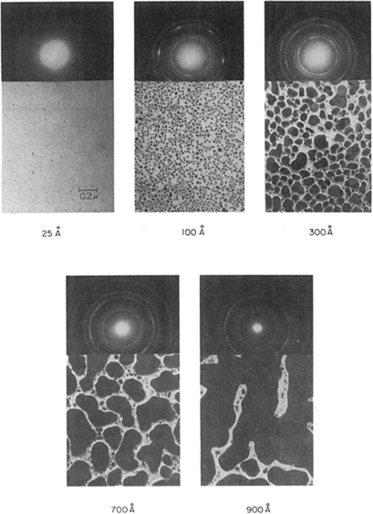
Figure 7-1 Transmission electron microscope images of nucleation, growth, and coalescence of Ag films on (111) NaCl substrates. Corresponding diffraction patterns are shown.
(From Ref. 2, courtesy of R. W. Vook.)
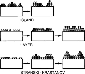
Many observations of subsequent film formation have pointed to three basic growth modes: (1) island (or Volmer–Weber), (2) layer (or Frank–Van der Merwe), and (3) Stranski–Krastanov, which are illustrated schematically in Fig. 7-2. Island growth occurs when the smallest stable clusters nucleate on the substrate and grow in three dimensions to form islands. This happens when atoms or molecules in the deposit are more strongly bound to each other than to the substrate. Metal and semiconductor films deposited on oxide substrates initially form such islands. The opposite characteristics are displayed during layer growth. Here the extension of the smallest stable nucleus occurs overwhelmingly in two dimensions, resulting in the formation of planar sheets. In this growth mode the atoms are more strongly bound to the substrate than to each other. The first complete monolayer is then covered with a somewhat less tightly bound second layer. Providing the decrease in bonding energy is continuous toward the bulk-crystal value, the layer growth mode is sustained. Single-crystal epitaxial growth of semiconductor films, a subject treated in Chapter 8, is the most important example of this growth mode. The layer plus island or Stranski–Krastanov (S-K) growth mechanism is an intermediate combination of the preceding two modes. In this case after forming one or more monolayers, subsequent layer growth becomes unfavorable and islands form. Film growth by the S-K mode is fairly common and has been observed in metal–metal andmetal–semiconductor systems.
This chapter traces the odyssey of nucleation events that starts with the clustering of isolated atoms on asubstrate, follows with the incorporation of additionally deposited atoms, and ends after the first several layers of film have formed. In this regime the nature of the substrate surface often plays an important role. We therefore start by discussing the nature ofsolid surfaces and see what happens when atoms impinge on them.
7.2 AN ATOMIC VIEW OF SUBSTRATE SURFACES
7.2.1 INTRODUCTION
Since they envelop and confine all solids including thin films and substrates, surfaces provide a key to understanding atomic behavior immediately beneath them as well as just above them. For many engineering purposes, thesefew atom layers collectively and seamlessly merge into what we call the “surface.” Real surfaces are usually contaminated with adsorbed gases and assorted compound layers. However, in this chapter surfaces will generally represent an atomically sharp interfacial demarcation between condensed-phase and gas-phase atoms.
There are many important reasons for studying the nature of clean surfaces. First of all, substrate surfaces usually provide the template for subsequent deposition and growth of thin films. In addition, surfaces also serve as the vehicle for imparting interfacial structural, mechanical, and physical properties to films. Secondly, assorted surface-analytical techniques are widely employed to reveal the chemical composition and structure of films. Through stimulation by photons, electrons, and ion beams, the electronic and physical structures of surface and near-surface atoms are altered in ways that can be detected, thus serving to fingerprint their identity and characterize their behavior. Thin films also confront the environment and interact chemically, mechanically, electrically, etc., with the ambient through their surfaces. And, as film thicknesses continue to shrink, which is the trend in many applications, a larger fraction of atoms will reside at the top film surface and bottom film–substrate interface; these surface atoms will then play increasingly greater roles in influencing the behavior of the atoms in between.
In this section we shall start by treating both the electronic and physical structures of subsurface atom layers of solids, and in particular, substrates. Then we will consider geometric placement of different atoms in the surface plane itself, our main interest being the first atomic layer of the film that deposits above the substrate surface plane. All in all perhaps only 15 Å of material at most is involved. Amazing as it seems, a profile through this vanishingly small thickness reveals that a minimum of two chemically different species interact in a continuum of bonding arrangements, and that at least three crystallographic structures can be differentiated. It is a testament to the great advances in surface science experimentation and theory that have enabled such distinctions to be made. An excellent review of the progress in this area to date is detailed in Surface Science: The First Thirty Years (Ref. 3). Importantly, through the electronic and optoelectronic devices it has made possible, surface science is intimately connected to the story of a “… technological revolution which is changing the world as we know it, transforming a planet into a global village.”
7.2.2 ELECTRONIC NATURE OF SURFACES
7.2.2.1 Metals
Solid-state physics has long considered the quantum nature of bulk crystalline solids. By now we are all familiar with the notion that the periodic electrostatic potential in lattices is responsible for electron energy bands and gaps, as well as the classification of solids into metals, semiconductors, and insulators. Although solutions to the Schrodinger wave equation for the many-body periodic potential are rarely possible, useful approximations exist. For example, assorted theoretical models, e.g., free electron, nearly free electron, tight binding, and pseudopotential, have yielded wave functions and energies for electron states in metals (Ref. 4). The electronic structure is commonly depicted by the band diagram shown in Fig. 1-9a, a representation applicable to bulk regions of the metal. At the surface, however, the assumed uniform positive potential due to ion cores is abruptly terminated. As a consequence, the mobile electrons within the bulk attempt to screen out the now unbalanced attractive potential at the surface. This results in an increased electron density at the surface which dies away rapidly in an oscillatory manner within the interior (Ref. 5). In solids with low electron densities the charge oscillations die away more slowly. Some of these features are shown in Fig. 7-3, where electron charge–density contours are plotted for nickel. At the surface the charge density is smeared out but it becomes periodic as the interior ion cores are reached. This smoothing of the surface charge is the compromise electrons strike when they lower both their potential and kinetic energies by respectively penetrating into the interior and by spreading out toward the surface.

Figure 7-3 Electron charge density contours around Ni (001) atoms near the surface.
(After F. J. Arlinghaus, J. G. Gay, and J. R. Smith, Phys. Rev. B21, 2055, (1980). Reprinted with the permission of John R. Smith.)
Surface or Tamm states were first predicted based on Schrodinger equation solutions to electrons in terminated periodic lattices. From the standpoint of quantum mechanics, the loss of three-dimensional lattice periodicity at the surface allows for quantum states that lie within the (bulk) energy gap (Ref. 6). Localized surface states are characterized by waves that travel parallel to the surface but not into the solid. When electron or hole charge occupies these states, electrostatic fields penetrate the interior and produce a variation of potential that is manifested as band bending. Adsorbed impurities, emergent dislocations, and surface relaxation (or reconstruction; see Section 7.2.4) also create surface states. But in all cases the extent of band bending in metals is generally negligible because there are sufficient numbers of mobile electrons to screen out or compensate for the surface-state charge; this is generally not true in semiconductors.
The work function (φ), an important surface property, is a consequence of the foregoing model. We may view φ as related to the difference in electron potential between that associated with the surface-charge relative to the average value within the bulk lattice. Thus q φ where q is the electronic charge, is the energy barrier electrons must surmount when leaving the solid. Measured values for φ in most elements cluster around 3.5 ± 1.5 V. Contributing to φis a charged double layer generated by the electron asymmetry at the surface. Alteration of this double layer due to adsorbed contaminants, alloying, or the crystallographic face exposed typically changes the magnitude of φby a few tenths of a volt.
7.2.2.2 Semiconductors
There are significant structural as well as electronic differences between semiconductor and metal surfaces. This fact is immediately apparent if we consider the interface between a (111), III–V compound semiconductor surface and vacuum shown in Fig. 7-4a. Forgetting distinctions between III–and V-type atoms for the moment, this ball-and-stick model is applicable to elemental semiconductors such as (111) silicon as well. The severed covalent bonds at the surface mean the presence of uncompensated charge and an electric field. However, dangling bonds from neighboring surface atoms bridge to complete the bonding requirements. In the process surface atoms shift position and the electrostatic energy in the vacuum is reduced. As we shall soon see (Sections 7.2.3.1 and 7.2.4.1), the surface reconstructs with important structural and property implications.

Figure 7-4a Model of (111) surfaces in the zinc blende crystal structure of a III–V compound semiconductor.
(From H. C. Gatos, Surf. Sci. 299/230, 1, (1994). Reprinted with the permission of Professor Harry C. Gatos, MIT.)
The same thing happens at III–V semiconductor surfaces but with interesting added twists. As the figure indicates, the surface consists entirely of Group V atoms (or light B atoms, e.g., As), but it could just as easily consist of Group III atoms (or dark A atoms, e.g., Ga). These unique and distinct surfaces arise because cuts can only be made between planes AA and BB. The reasons for such cuts are: (a) only one bond between atoms needs to be disrupted and (b) the surface atoms remain triply bonded to the lattice. Other cuts such as those between AA and B’B’ are not possible because three bonds must be severed and resultant surface atoms are singly bonded to the lattice. For the BB, so-called (111) surface, we note that only three of five valence electrons in each arsenic atom are attached or bonded, while on an AA (111) surface all three of boron’s valence electrons are bonded. As a consequence, the As surface is more electronically active than the Ga surface, and can, for example, be smoothed and polished more readily by etching. In contrast, Ga surfaces etch slowly and tend to be rougher. Such differences lead to varied epitaxial phenomena when films are deposited on these surfaces.
Unlike metals, two bands–a lower valence as well as an upper conduction band–play important roles in semiconductors and devices based on them. Another difference is the band bending that occurs at semiconductor surfaces that contact other materials such as insulators, as shown in Fig. 7-4b. Band bending or the absence of a flat band condition means that a nonzero electrical potential ψs exists at the surface. What generates ψs are the severed covalent bonds at the semiconductor surface which are essentially localized surface-states that trap electrons or holes. Together with ionized donors or acceptors they create a spatially varying charge distribution near the surface. The situation parallels that of the plasma-sheath region (Section 4.3.5). A solution to the Poisson–Boltzmann equation in one dimension essentially yields a form of ψ similar to that for the electrostatic potential in a plasma (e.g., Eq. 4-17, also problem 5 in Chapter 4). Because there are relatively few carriers to shield surface charge, band bending is much more pronounced in semiconductors than in metals, e.g., the electrostatic potential typically penetrates ∼ 1 μm below the surface. A space charge region is said to exist where the bands are bent. Within it the semiconductor exhibits dielectric behavior and supports the internal electric-field, i.e.,![]() that makes possible rectifying action at a p–n junction.
that makes possible rectifying action at a p–n junction.
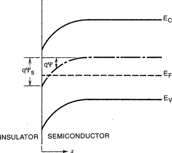
Figure 7-4b Energy band diagram at the surface of a p-type semiconductor. The potential ψ is defined to be zero in the bulk but assumes a nonzero value at the surface that depends on the phase contacting the semiconductor, e.g., vacuum, SiO2, or other semiconductor.
(After S. M. Sze, Physics of Semiconductor Devices, 2nd ed. John Wiley & Sons, New York, 1981.)
For semiconductor surfaces to perform electrical functions in devices they are often contacted by either insulating, dielectric, or conducting thin films.
In silicon, for example, these films are invariably either grown or deposited SiO2, and deposited metals (M) that serve as electrical contacts. Because Si–SiO2 and M–Si structures are of such great technical importance, these interfaces are perhaps the most studied in all of physical science. As a result there is a broad accessible literature on interfacial Si–SiO2 charge and barriers to electron flow across M–Si contacts; for this reason these topics will not be discussed here.
7.2.3 SURFACE STRUCTURES
7.2.3.1 Introduction
As we have already seen, minimization of the overall electronic and bonding energies in the topmost atom layers causes the surface crystallography to differ from that of the bulklike interior as suggested by the schematic cross-sectional views of Fig. 7-5. If the surface structure is the predictable extension of the underlying lattice, we have the case shown in Fig. 7-5a. However, the loss of periodicity in the vertical direction alters surface electronic properties and leaves energetic broken bonds. It is then more likely that the structure shown in Fig. 7-5b will prevail. The absence of bonding forces to underlying atoms results in new equilibrium positions which deviate from those in the bulk lattice. A disturbed surface layer known as the “selvedge” may then be imagined. Within this layer the atoms relax in such a way as to preserve the symmetry of the bulk lattice parallel to the surface, but not normal to it. A more extreme structural disturbance is depicted in Fig. 7-5c, where surface atoms rearrange into a structure with a symmetry that differs from that of the bulk solid. This phenomenon is known as reconstruction and can alter many surface structure-sensitive properties, e.g., chemical, electrical, optical, and sorption behavior.
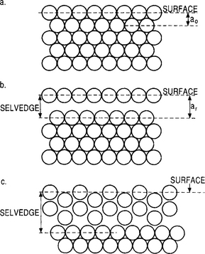
Figure 7-5 Schematic cross-sectional views of close-packed atomic positions at a solid surface. (a) Bulk exposed plane. (b) Atomic relaxation outward. (c) Reconstruction of outer layers.
(From Ref. 5, © Oxford University Press, by permission.)
Whereas atomic positioning in the selvedge cross-section is not amenable to simple analysis, the crystallography in the surface plane is, and we now proceed to discuss it. In particular, we are interested in such surfaces covered by a periodic array of adsorbed atoms (adatoms).
7.2.3.2 Crystallography of Substrate Meshes and Adatom Arrays
Just as there are 14 Bravais lattices in three dimensions, so there are just five unit meshes or nets, corresponding to a two-dimensional surface as shown in Fig. 7-6. Points representing atoms may be arranged to outline (1) squares, (2) rectangles, (3) centered rectangles, (4) rhombi, and (5) parallelograms with included angles of 60° and 120°. Miller-type indices are used to denote atom coordinates, directions, and distances between lines within the surface.

Consider a mesh of substrate atoms that is covered with adatoms arrayed in a monolayer pattern. The methodology for identifying the structural geometry employs simple vector concepts (Refs. 5, 7). Vectors describing the adsorbate positions (b) are simply related to those of the substrate lattice (a). Possessing components bi and ai, with i = 1,2 denoting the x and y directions, we may generally write
Terms Mij denote the components of the transformation matrix between adatom and substrate coordinates. Let us apply these equations to Fig. 7-7a where a square monolayer pattern of adatoms denoted by (![]() ) covers a net of substrate atoms represented by • (dots). This combination might correspond to the early growth of an epitaxial layer on the (100) plane of a BCC or FCC crystalline substrate; for the latter, however, a larger face-centered cell must be chosen. In the case shown, b1 = 2a1 and b2 = 2a2.
) covers a net of substrate atoms represented by • (dots). This combination might correspond to the early growth of an epitaxial layer on the (100) plane of a BCC or FCC crystalline substrate; for the latter, however, a larger face-centered cell must be chosen. In the case shown, b1 = 2a1 and b2 = 2a2.

Figure 7-7 Atomic positions of adatoms (![]() ) relative to substrate atoms • arrayed on a (100) simple cubic plane. (a)P(2 × 2) overlayer structure. (b)C(2 × 2) centered lattice overlayer or
) relative to substrate atoms • arrayed on a (100) simple cubic plane. (a)P(2 × 2) overlayer structure. (b)C(2 × 2) centered lattice overlayer or ![]() structure. (c)P(1 × 2) overlayer structure. (d) P(2 × 1) overlayer structure. Corresponding reciprocal lattices for (c) and (d) are shown (x refers to adatoms).
structure. (c)P(1 × 2) overlayer structure. (d) P(2 × 1) overlayer structure. Corresponding reciprocal lattices for (c) and (d) are shown (x refers to adatoms).
and we speak of a P(2 × 2) overlayer structure, where P indicates a primitive unit cell effectively containing only one atom. If, for example, this structure physically corresponds to a deposit of sulfur atoms on (100) Fe, the notation would be Fe(100) P(2 × 2)-S. In a similar vein, suppose there is an additional adatom positioned centrally as shown in Fig. 7-7b. Intuition would suggest that such a structure be identified asC(2 × 2) where C denotes the centered lattice. The matrix notation for the dashed primitive cell in this case is
Because the overlayer primitive cell dimensions are ![]() times larger and rotated relative to substrate unit cell, an alternative notation is
times larger and rotated relative to substrate unit cell, an alternative notation is ![]() where R stands for rotation.
where R stands for rotation.
Consider now the repetitive rectangular adatom cell pattern in Fig. 7-7c where b1 =a1 and b2 = 2a2. Therefore,
and the overlayer is denoted by P(1 × 2). Similarly, Fig. 7-7d shows an overlayer of the same geometry but rotated 90° with respect to case c; the notation would be P(2 × 1).
It should be noted that there is a certain ambiguity in identifying overlayers. We have only considered caseswhere the adatoms fall directly above substrate atoms. But adatoms may also lie in pockets between substrate-atom sites. This can happen, for example, by shifting each adatom by ½a1 and ½a2. But vector operations are independent of the choice of origin and such overlayers would be identified by exactly the same notations as before, e.g., P(2 × 2),P(1 × 2).
7.2.3.3 The Reciprocal Lattice
It is the geometry of the reciprocal lattice, not that of the real lattice, which appears as the physical image in diffraction patterns. As the name implies, the reciprocal lattice has dimensions and features which are “inverse” to those of the real lattice. In rectangular coordinates long dimensions in real space appear rotated 90° and areshortened in inverse proportion within the reciprocal space. The relation between b1 and b2 and the reciprocal vector components b*1 and b*1 of the unit mesh in the reciprocal lattice is expressed by
and similarly,
where δij = 0 if i ≠ j and δij = 1 if i = j.
Reciprocal lattices corresponding to the real space structures of Figs. 7-7c and 7-7d are sketched intuitively in the same figure. The scale is arbitrary, but the lattice periodicity and symmetry are preserved. When two adatom orientations, P(2 × 1) and P(1 × 2) are admixed in roughly equal proportions, as might happen during deposition, the reciprocal lattices from each simply superimpose. It is left as an exercise for the reader to sketch the resultant pattern.
Two classic techniques for analyzing the structure of crystalline surfaces and epitaxial films in particular, are low-energy electron diffraction (LEED) and reflection high-energy electron diffraction (RHEED). Both are described in the next chapter in connection with epitaxial films and require the unfamiliar visualization in reciprocal space. Leaving less to the imagination is scanning tunneling microscopy (STM), an important new technique that provides direct images of adatoms on substrate surfaces. Many of our present notions of surface crystallography have emerged through LEED and STM methods. In the next two sections as well as one at the chapter’s end (Section 7.5.4) we shall see how STM has enhanced our understanding of semiconductor surfaces.
7.2.4 RECONSTRUCTED SILICON SURFACES
7.2.4.1 Crystallography of (001) Si
On a clean (001) Si surface, atoms are surprisingly not arranged according to the much reproduced bulk diamond-cubic lattice structure where the nearest-neighbor atom separation is 0.385 nm. Instead, the isotropic face-centered square array of Si atoms assumes an anisotropic reconstructed structure of lower symmetry (Ref. 8) possessing two characteristic directions. These lie in the surface plane either along or perpendicular to dimer (paired atom) rows in orthogonal 〈110〉 orientations. The parallel dimer rows aligned at 135° with respect to the page horizontal, are easily visible in the STM image of Fig. 7-8a.

Figure 7-8 (a) Scanning tunneling microscope image of parallel dimer rows.
(From Ref. 35.) (b) Schematic side view of the reconstructed (001) Si surface having a (2 × 1) structure. (c) Top view of reconstructed (2 × 1) Si surface. The intensified unit cell measures 0.385 nm × 0.770 nm. (From Ref. 8.) (Reprinted with the permission of Max G. Lagally.)
More will be said about STM methods in Chapter 10. Suffice it to say that in this technique a metal probe tip sharpened to atomic dimensions is brought to within a few angstroms of the surface and scanned over its periodically bumpy atomic terrain, much like a stylus over a record. The current that flows between probe and surface reflects the topography of individual atoms on surfaces as well as the geometry of terraces and ledges or steps on the substrate surface.
Schematically shown in both side and top views of Figs. 7-8b and 7-8c is the (2 × 1) reconstructed surface structure on (001) Si. In these figures the position of silicon atoms, differentiated by circle size, is shown at three successive levels. Within dimers the Si atoms would like to merge even closer together but are restrained from doing so by surrounding atoms. Therefore, a tensile stress develops in the dimer-bond direction; similarly along the dimer row a smaller tensile or perhaps compressive stress is expected. Because of stress anisotropy the reconstructed surface of (001) Si decomposes into two alternating (2 × 1) terrace-like domains with monatomic steps at the boundaries. Dimer rows rotate 90° as successive terraces are accessed giving rise to two types of monatomic steps. The so-called SA step is parallel to upper-terrace dimer rows, while SB steps are perpendicular to these same rows. Because it is difficult to disrupt the linearity of dimer rows, the energy to form a kink in an SA step is higher than for an SB step. Thus SA steps tend to appear smooth while SB steps are rough. What happens when Si atoms deposit on such a terraced substrate is discussed in Section 7.5.4.1.
7.2.4.2 Crystallography of (111) Si
Reconstruction of (111) Si surfaces into (7 × 7) structures was first observed in LEED patterns (Ref. 9) similar to those shown in Fig. 8-33a. Disbelieved at first, these beautiful patterns were attributed to contaminated surfaces. It was some 25 years later that the now ubiquitous STM image of (111) Si shown in Fig. 7-9 independently confirmed the existence of the (7 × 7) reconstruction. Unfolding the surface and subsurface atomic positions that give rise to such a complex crystallographic structure is a formidable task. A minimum of 49 atom positions are involved and since the reconstruction occurs over several layers many more atom coordinates (perhaps hundreds) must be specified. Detailed crystallographic models for (7 × 7) Si have been proposed. This subject is clearly beyond our scope and therefore, the interested reader is referred to Refs. 10 and 11.
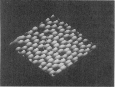
Figure 7-9 Figure 7-9 Scanning tunneling microscope image of the reconstructed (7 × 7) surface of (111) Si.
(Courtesy of Y. Kuk, AT&T Bell Laboratories.)
We shall return to the reconstructed (001) and (111) Si surfaces at the end of the chapter where the early stages of film nucleation on them areconsidered.
7.2.5 Adsorption Reactions on Solid Surfaces
Let us now take the pristine substrate surfaces we have been considering and expose them to gas particles. This is what occurs, for example, in thin-film deposition processes or during the operation of catalysts (Ref. 12). The first thing that happens is surface adsorption–the process in which impinging atoms and molecules enter and interact within the transition region between the gas phase and substrate surface (Ref. 13). Two kinds of adsorption processes, namely physical (physisorption) and chemical (chemisorption), can be distinguished depending on the strength of the atomic interactions. If the particle (molecule) is stretched or bent but retains its identity, and van der Waals forces bond it to the surface, then we speak of physisorption. However, chemisorption is involved whe particle changes its identity through ionic or covalent bonding with substrate atoms. The two sorptions can be quantitatively distinguished on the basis of adsorption heats or energies, Ep and Ec, for physisorption and chemisorption, respectively. Typically Ep ∼0.25 eV while Ec ∼1–10 eV.
Individual physi- and chemisorption processes can be visualized in the respective curves P and C of Fig. 7-10, representing the potential energies of interaction as a function of distance r(see Fig. 1-8). It is evident that physisorbed particles achieve equilibrium further from the surface (i.e., at r = rp) than chemisorbed species (at r = rc). In addition to Ep and Ec we must consider the dissociation energy of molecules, Edis. If Edis is less than Ec, dissociative chemisorption is thermodynamically possible. When both adsorption processes occur the curves merge and assume a roller-coaster shape with an effective energy barrier Ea that governs the rate of the transition from the physisorbed to chemisorbed states. In the subsequent treatment of film nucleation a composite energy of desorption (Edes) that integrates over all desorption states will be used. Similarly, an energy of adsorption (Eads) related to either Ep or Ec, or some combination of these, can be defined.
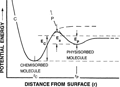
Figure 7-10 Model of physisorption and chemisorption processes in terms of the interaction potential between adsorbate and surface vs distance.
7.2.5.1 Adsorption Effects
To apply these ideas to deposition processes, let us consider a vapor phase containing potential adatoms at a partial pressure P. During adatom condensation on the substrate, the net time (t) rate of surface coverage (θ) is given by
where θ assumes values between 0 (no deposit) and 1 (monolayer coverage). The first term reflects the rate of adatom coverage at the available fraction of unoccupied surface sites; this process is proportional to the adsorption rate constant kads, which in turn varies as kads ∼exp− (Eads/kBT). Likewise, adatom desorption is directly proportional to the product of the rate constant kdes ∼exp− (Edes/kBT) and the coverage. Integration yields
where the equilibrium constant K = kads/kdes. At very long times, the equilibrium coverage is given by θ = KP/(1 + KP), a relation known as the Langmuir isotherm. When KP ![]() 1 the surface coverage is unity.
1 the surface coverage is unity.
7.2.5.2 Statistical Theory Surface Roughening
Given an adatom population, values of θ have theoretical implications for the morphology of the surface deposit. To see why, we note that substrate sites are either occupied by adatoms or unoccupied. Furthermore, adatoms lower their internal energy by bonding to the substrate as well as each other, and raise the configurational entropy through random occupation of substrate sites. We wish to predict the equilibrium state of a system governed by the eternal thermodynamic tug (Eq. 1-5) between changes in enthalpy, or equivalently, internal energy (U) in this case, and entropy (S). Taking the Gibbs free energy of the adatoms as G = U − TS, well-established concepts of statistical mechanics provide U and S in terms of θ, yielding
where ns is the number of surface sites. Equations of this form have long been used in many contexts within metallurgy and solid-state physics, e.g., theories of binary alloying and magnetism (Ref. 14). More relevant to our case, Jackson et al. (Ref. 15) showed that this very equation described smooth vs rough growth of crystals from melts. There was thus a precedent for Tsao (Ref. 16), who more recently applied Eq. 7-5 to the issue of smooth vs rough growth, but in vapor deposited layers. Only the first term (U) on the right will be derived, since the expression for S is given in many places (Ref. 14). It is assumed that when an adatom attaches to the surface one downward vertical bond is annihilated during reaction with a substrate atom, one dangles upward, and the remaining four bonds dangle laterally. For an individual bond energy of w, the adatom has a total energy of 4w. If the adatom now associates with other like adatoms, the energy decreases by 4θw because there are 4 reaction sites and a probability θ that each will be occupied. The energy per adatom is 4w − 4θw = 4w(1 − θ), and therefore the change in internal energy per atom site is the product of the latter and the coverage, or 4wθ(1 − θ).
Thermodynamic equilibrium is achieved when free energy (G/ns) is minimized or d(G/ns)/dθ = 0. Upon differentiation,
When kBT/4w is plotted vs θ a kind of phase diagram emerges with a symmetric miscibility gap. Thus at low temperatures for θ = 0.5, separation into two phase regions, a near-zero coverage (θ ![]() 0) layer and a near-unity coverage (θ
0) layer and a near-unity coverage (θ ![]() 1) layer, occurs; in either case the surface appears to be nearly atomically flat. However, a roughened surface emerges at elevated temperatures reflecting the dominance of entropy effects. At the roughening temperature (Tr), a transition occurs between the phase-separated smooth adlayers and the microscopically rough adlayer. For a value of θ = 0.5, Tr is calculated to be 2w/kB; physically, w is estimated to be ∼⅓ΔHs where ΔHs is the sublimation energy (typically 2–5 eV). This leads to unreasonably large values of Tr, indicating the rough qualitative nature of the theory.
1) layer, occurs; in either case the surface appears to be nearly atomically flat. However, a roughened surface emerges at elevated temperatures reflecting the dominance of entropy effects. At the roughening temperature (Tr), a transition occurs between the phase-separated smooth adlayers and the microscopically rough adlayer. For a value of θ = 0.5, Tr is calculated to be 2w/kB; physically, w is estimated to be ∼⅓ΔHs where ΔHs is the sublimation energy (typically 2–5 eV). This leads to unreasonably large values of Tr, indicating the rough qualitative nature of the theory.
We now shift direction from this focus on atomistic details of crystalline surfaces, and in the next few sections treat a complementary macroscopic view of layers deposited on substrates. Such an approach is often more useful pedagogically in describing film formation and growth effects. When it comes to epitaxial films (in Chapter 8), however, a microscopic view is again more appropriate.
7.3 THERMODYNAMIC ASPECTS OF NUCLEATION
7.3.1 SCOPE
Paradoxically, nucleation events which may only involve very few atoms can be profitably described in terms of classical thermodynamics, a subject that deals with the continuum behavior of many atoms. Among the questions addressed in this section are:
1. Under what conditions are nuclei of thin-film deposits thermodynamically stable?
2. What role do surface energies of films and substrates play in nucleation events?
3. Under given deposition conditions (i.e., vapor supersaturation), how large are the nuclei predicted to be, and what is the energy barrier that must be surmounted in their formation?
4. How are island, planar, and S-K growth modes rationalized thermodynamically?
5. What influence do film deposition rate and temperature have on nucleation energetics and nucleus size?
However, issues related to atomic-scale nucleation events, the rates at which they occur, and the numbers of stable nuclei produced per unit time are not easily amenable to thermodynamics and will be treated in subsequent sections. Since surface energies of materials play a key role in these discussions, this subject is a good place to start.
7.3.2 SURFACE ENERGIES
In the well-known capillarity or droplet theory of homogeneous nucleation, a solid nucleates from a prior unstable liquid or vapor phase by respectively establishing a solid–liquid (s-l) or solid–vapor (s-v) interface. Associated with these interfaces or surfaces are corresponding interfacial energies. Atoms at free surfaces are more energetic than atoms within the underlying bulk because they make fewer bonds with surrounding atoms and are thus less constrained. The difference in interatomic energy of atoms at these two locations is the origin of surface energy. Alternatively, there is a thermodynamic driving force to reduce the number of necessarily cut, dangling bonds at the surface through rebonding between atoms. We may then equivalently view the surface energy γ (J/m2) in terms of the energy reduction per unit area.
In a recommended discussion of surface energies of solids by Tu et al. (Ref. 17) a number of issues relevant to surfaces are raised. With respect to material classes and systematics, metals have higher surface energies than oxides, alkali halides, sulfides, and organic substances. For virtually all elements in the liquid and solid states the surface energies roughly span the range 0.2 to 3 J/m2 with 1 J/m2 (= 1000 erg/cm2) being typical. The higher values are associated with the transition metals while the lower values are indicative of alkali and divalent metals, metalloids, and inert gases. For organic and aqueous solutions γ is often less than 100 mJ/m2. Furthermore, the surface energy drops slightly with temperature T; typically, dγ/dT ∼ −0.05 mJ/m2-°C.
Surface energies are often interchangeably called surface tensions. These terms are not strictly identical although units of the latter, i.e., force/length, are equivalent to energy/area. The basic definition of surface energy is related to the reversible work (dW) on a material when its surface area (A) is increased, or dW = γdA. Surfaces can alter their energies through change in either A or γ. The latter possibility implies altering atomic arrangements or reconstructing the surface and may be thought of as the work in mechanically stretching or straining the surface. For solids, surface stresses are thus involved, but these vanish in liquids because they cannot support strains. It is the shortening of the surface bond length plus the effective conversion of bulk to surface bonds that essentially causes liquid mercury to ball up; in the process A is reduced. We shall make no further distinction between surface energy and surface tension.
7.3.3 CAPILLARITY THEORY OF HETEROGENEOUS NUCLEATION
We have already considered a simple model for homogeneous nucleation of a condensed phase from a prior supersaturated vapor (see Section 1.7). Homogeneous nucleation, although rare in other contexts, occurs with some frequency in CVD reactors where too highly supersaturated gases rain “snow” down on substrates. The process is easy to model since it occurs without benefit of the complex heterogeneous sites that exist on an accommodating substrate surface. In a similar spirit we shall extend this capillarity theory to the case of heterogeneous nucleation of a condensed film on a substrate. Capillarity theory (Refs. 17-19) possesses the mixed virtue of yielding a conceptually simple qualitative model of film nucleation which is, however, quantitatively inaccurate. The lack of detailed atomistic assumptions gives the theory an attractive broad generality with the power of creating useful connections among such variables as substrate temperature, deposition rate, and critical film nucleus size.
We start by assuming that film forming atoms or molecules in the vapor phase impinge on the substrate creating nuclei of mean dimension r. The free-energy change accompanying the formation of such an aggregate is given by
As in homogeneous nucleation the chemical free-energy change per unit volume, ΔGv, drives the condensation reaction. There are several interfacial tensions, γ, to contend with now and these are identified by the subscripts f, s, and v representing film, substrate, and vapor, respectively. A pair of subscripts refers to the interface between the indicated phases. For the spherical cap-shaped solid nucleus shown in Fig. 7-11 the curved surface area (a1r2), the projected circular area on the substrate (a2r2), and the volume (a3r3) are involved, and the respective geometric constants are a1 = 2π(1 − cos θ), a2 = π sin2θ, and ![]() .
.
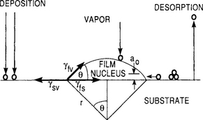
Figure 7-11 Schematic of basic atomistic nucleation processes on substrate surface during vapor deposition.
The mechanical equilibrium among the horizontal components of the interfacial tensions or forces surrounding the nucleus yields Young’s equation,
Importantly, the contact or wetting angle θ, which figures prominently in the formulas for r* and ΔG* developed later, depends solely on the surface properties of the involved materials.
Returning now to Eq. 7-6, we note that any time a new interface appears there is an increase in surface free energy and hence the positive sign for the first two surface terms. Similarly the loss of the circular substrate–vapor interface under the cap implies a reduction in system energy and a negative contribution to ΔG. Thermodynamic equilibrium is achieved when dΔG/dr = 0, which occurs at a critical nucleus size r = r* given by
Correspondingly, ΔG evaluated at r = r* is
Both r* and ΔG* scale in the manner shown in Fig. 1-20. An aggregate smaller in size than r* disappears by shrinking, lowering ΔG in the process. Critical nuclei grow to supercritical dimensions by further addition of atoms, a process which lowers ΔG still more. In heterogeneous nucleation the accommodating substrate catalyzes vapor condensation by lowering the energy barrier ΔG* through a reduction of the contact angle. After substitution of the geometric constants, it is easily shown that ΔG* is essentially a product of two factors, i.e.,
The first is the value for ΔG* derived for homogeneous nucleation. It is modified by the bracketed term, a wetting factor dependent on θ which has the value of zero for θ = 0 and unity for θ = 180°. When the film wets the substrate, there is no barrier to nucleation. At the other extreme of dewetting, ΔG* is maximum and equal to that for homogeneous nucleation.
The preceding formalism provides a generalized framework for inclusion of other energy contributions. If, for example, the film nucleus is elastically strained throughout because of the bonding mismatch between film and substrate, then a term a3r3ΔGs, where ΔGS is the strain free-energy change per unit volume, would be appropriate. In the calculation for ΔG*, the denominator of Eq. 7-9 would then be altered to ![]() (ΔGV+ ΔGS)2. Because the sign of ΔGV is negative while ΔGS is positive, the overall energy barrier to nucleation increases in such a case. If, however, deposition occurred on an initially strained substrate, i.e., one with emergent cleavage steps or screw dislocations (see Fig. 8-10), then stress relieval during nucleation would be manifested by a reduction of ΔG*. Substrate charge and impurities would similarly influence ΔG* by affecting terms related to either surface and volume electrostatic, chemical, etc., energies.
(ΔGV+ ΔGS)2. Because the sign of ΔGV is negative while ΔGS is positive, the overall energy barrier to nucleation increases in such a case. If, however, deposition occurred on an initially strained substrate, i.e., one with emergent cleavage steps or screw dislocations (see Fig. 8-10), then stress relieval during nucleation would be manifested by a reduction of ΔG*. Substrate charge and impurities would similarly influence ΔG* by affecting terms related to either surface and volume electrostatic, chemical, etc., energies.
The most important thing to remember about ΔG* is its strong influence on the density (N*) of stable nuclei that can be expected to survive. Based on our previous experience (Eq. 1-3) of associating the probable concentration of an entity with its characteristic energy through a Boltzmann factor, it is appropriate to take
where ns is the total nucleation site density. We shall return to this equation subsequently.
7.3.4 FILM GROWTH MODES
Young’s equation (Eq. 7-7) provides a way to distinguish and better understand the three modes of film growth displayed in Fig. 7-1. For island growth, θ > 0, and therefore,
If γfs is neglected, this relation suggests that island growth occurs when the surface tension of the film exceeds that of the substrate. This is why deposited metals tend to cluster or ball up on ceramic or semiconductor substrates.
In the case of layer growth the deposit “wets” the substrate and θ ![]() 0. Therefore,
0. Therefore,
A special case of this condition is ideal homo- or “auto-epitaxy.” Because the interface between film and substrate essentially vanishes, γfs = 0. High-quality epitaxial films require the avoidance of any disruption to layer growth. Superlattices composed of alternating A and B epitaxial films ordered in a stack represent a particularx challenge in this regard. Sequential depositions mean A deposited on a B film substrate followed by B deposited on an A film substrate. This stacking asymmetry is often not a problem when A and B are heteroepitaxial compound semiconductors; high-performance lasers have been fabricated in this way. Although roughly equal surface energies are involved here, this is not usually the case in metal–metal or metal–semiconductor superlattices. In general, materials with low surface energy will wet substrates with a higher surface energy. Thus Benjamin Franklin observed that a little oil smoothed the surface roughness of a large water pond. In this case the very thin oil film that formed dramatically modified the surface properties of water.
Lastly, for S-K growth, initially at least,
In this case the strain energy per unit area of the film overgrowth is large with respect to γfv permitting nuclei to form above the initial layers. The transition from two- to three-dimensional growth which typically occurs after 5–6 monolayers is not completely understood; any factor which disturbs the monotonic decrease in binding energy characteristic of layer growth may be the cause. For example, because of film–substrate lattice mismatch, strain energy accumulates in the growing film. When released, the high energy at the deposit intermediate-layer interface may trigger island formation.
7.3.4.1 Morphological Stability of Strained Layers
To address strain (free) energy (GS) semiquantitatively we note that elasticity theory (Eq. 1-45) suggests GS = ½Yε2 where Y is the elastic modulus of a layer and ε is its strain. A useful measure of ε at the interface between a film and substrate is the lattice mismatch strain or simply misfit, ![]() , defined as
, defined as ![]() , where a0 is the lattice parameter and f and s refer to the film and substrate, respectively. As we shall see, the quantity
, where a0 is the lattice parameter and f and s refer to the film and substrate, respectively. As we shall see, the quantity ![]() assumes an important role in epitaxy (Chapter 8).
assumes an important role in epitaxy (Chapter 8).
Rather than view the breakdown of epitaxy due to dislocation generation as in Section 8.3.1, let us consider the critical film thickness beyond which a planar film surface roughens due to the growth of islands. This creates a morphological instability that can be treated in terms of macroscopic heterogeneous nucleation theory. Following Wessels (Ref. 20), the net free energy change for the nucleation of a hemispherical island (not spherical cap) on top of a growing, strained epitaxial layer of thickness h is given by
In the process the island is assumed to be incoherent (or relaxed) while the epilayer partially relaxes. By reference to Eq. 7-6, the volume free energy of the island and interfacial and strain energy interaction between the island and epitaxial layer are, respectively, ΔGV, γ, and ΔGS. The term ΔGS is interpreted as the difference in epilayer strain energy per unit area after the island nucleates (½Yε2h) relative to that in the epilayer prior to island nucleation (![]() ). Therefore,
). Therefore, ![]() where ε is the mean misfit in the strained film and A (= πr2) is the area affected by strain. As before, the critical nucleus radius (r*) is determined by the condition that dΔG/dr = 0. Therefore,
where ε is the mean misfit in the strained film and A (= πr2) is the area affected by strain. As before, the critical nucleus radius (r*) is determined by the condition that dΔG/dr = 0. Therefore,
and in the limit that r* = 0, the critical film thickness (h*) for the onset of the rough island morphology (e.g., S-K growth) is
This relation implies that h* varies approximately as ![]() . For InGaAs on GaAs, Wessels suggests that
. For InGaAs on GaAs, Wessels suggests that ![]() holds after substituting appropriate constants. When
holds after substituting appropriate constants. When ![]() there is a transition from 2-D layer to 3-D island film growth.
there is a transition from 2-D layer to 3-D island film growth.
Now we may better understand Fig. 7-12, which distinguishes the regimes of influence for the three film growth modes in terms of surface energy ratio W(W = (γs − γf)/ γs) and ![]() . As noted earlier, when γf > γs, i.e., W < 0, island growth dominates. But its range of dominance expands when there is additional misfit present. Layer growth is possible only when W > 0; surprisingly, however, this growth mechanism can tolerate a small amount of misfit, a fact that makes strained-layer epitaxy feasible. In between island and layer film morphologies, and competing with them, is the S-K growth mode.
. As noted earlier, when γf > γs, i.e., W < 0, island growth dominates. But its range of dominance expands when there is additional misfit present. Layer growth is possible only when W > 0; surprisingly, however, this growth mechanism can tolerate a small amount of misfit, a fact that makes strained-layer epitaxy feasible. In between island and layer film morphologies, and competing with them, is the S-K growth mode.

Figure 7-12 Stability regions of the three film growth modes in coordinates of surface energy difference between film and substrate (vertical) and lattice misfit (horizontal).
(From K. N. Tu, J. W. Mayer, and L. C. Feldman, Electronic Thin Film Science for Electrical Engineers and Materials Scientists, Macmillan, 1992. Originally published in IBM J. Res. Develop. Reprinted with the permission of Professor K. N. Tu.)
7.3.5 Nucleation Dependence on Substrate Temperature and Deposition Rate
Substrate temperature and deposition rate ![]() (atoms/cm2-s) are among the chief variables affecting deposition processes. Calculating their effect on r*and ΔG* is both instructive and simple to do. First we assume that
(atoms/cm2-s) are among the chief variables affecting deposition processes. Calculating their effect on r*and ΔG* is both instructive and simple to do. First we assume that ![]() is proportional to PV in Eq. 1-38 so that
is proportional to PV in Eq. 1-38 so that
where ![]() is the equilibrium evaporation rate from the film nucleus at the substrate temperature. Assuming an inert substrate, i.e., γfv = γfs, direct differentiation of Eq. 7-8 yields (Ref. 18)
is the equilibrium evaporation rate from the film nucleus at the substrate temperature. Assuming an inert substrate, i.e., γfv = γfs, direct differentiation of Eq. 7-8 yields (Ref. 18)
Assuming typical values, γfv = 1 J/m2 and ∂γfv/∂T = −0.05 mJ/m2-K. An estimate for ∂ΔGV/∂T is the entropy change for vaporization, which is roughly 8 × 10⁶ J/m3-K for many metals. As long as ![]() direct substitution shows that
direct substitution shows that
Similarly, by the same assumptions and arguments
It is also simple to show that
Direct chain-rule differentiation using Eqs. 7-8 and 7-18 yields
Since ΔGV is negative, the overall sign is negative. Similarly, it is easily shown that
The preceding four inequalities have interesting implications and summarize a number of common effects observed during film deposition. From Eq. 7-20 we note that a higher substrate temperature leads to an increase in the size of the critical nucleus. Also, a discontinuous island structure is predicted to persist to a higher average coverage than at low substrate temperatures. The second inequality (Eq. 7-21) suggests that a nucleation barrier may exist at high substrate temperatures whereas at lower temperatures it is reduced in magnitude. Also, because of the exponential dependence of N* on ΔG*, the number of supercritical nuclei decreases rapidly with temperature. Thus, a continuous film will take longer to develop at higher substrate temperatures. From Eq. 7-22 it is clear that increasing the deposition rate results in smaller islands. Because ΔG* is also reduced, nuclei form at a higher rate suggesting that a continuous film is produced at lower average film thickness. If for the moment we associate a large r* and ΔG* with being conducive to large crystallites or even monocrystal formation, such conditions prevail at high substrate temperatures and low deposition rates. Alternately low substrate temperatures and high deposition rates yield polycrystalline deposits. These simple guidelines summarize much practical deposition experience in a nutshell.
A plot of these structural zones as a function of deposition rate and substrate temperature is shown in Fig. 7-13 for Cu films deposited on a (111) NaCl substrate. Maps of this sort have been graphed for other film–substrate combinations. In semiconductor systems a regime of amorphous film growth is additionally observed when ![]() is large and T is low.
is large and T is low.
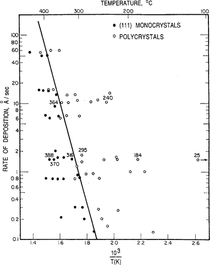
Figure 7-13 Dependence of microstructure on deposition rate and substrate temperature for Cu films on (111) NaCl. Some substrate temperatures are noted.
(Reprinted with permission from the Metals Society. From Ref. 2, courtesy of R. W. Vook.)
Despite the qualitative utility of capillarity theory, it is far from being quantitatively correct. For example, let us estimate the value of r* for a typical metal film at 300 K. To simplify matters the homogeneous nucleation formula, r* = −2γ/ΔGv, will be used where ΔGv = −kBT/Ωln Pv/Ps. Assuming Ω = 20 × 10−30/m3, γ = 1 J/m2, Pv = 10−3 torr, and Ps = 10−10 torr, then r* = −2(1.0)/−{[1.38 × 10−23 × 300/20 × 10−30]ln[10−3/10−10]} or 0.6 nm.
A nucleus of this size contains just a few atoms, and it is therefore doubtful that continuum concepts such as surface tension and nucleus radius have much significance. It is more realistic to interpret vapor condensation phenomena in terms of a heterogeneous nucleation theory based on atomistic modeling. This is one of the topics considered in the next section.
7.4 KINETIC PROCESSES IN NUCLEATION AND GROWTH
7.4.1 SCOPE
Among the questions addressed in this section are:
1. What is the nucleation rate ![]() and how does it depend on time, temperature, deposition rate, and the nature of the film and substrate?
and how does it depend on time, temperature, deposition rate, and the nature of the film and substrate?
2. Once formed, what are the possible mechanisms for subsequent growth and coalescence of nuclei?
3. What is the time dependence for the growth and coalescence of nuclei?
In particular, distinctions between the macroscopic (e.g., capillarity) and microscopic (atomistic) views of these processes will be stressed. For the most part theoretical modeling is emphasized.
7.4.2 NUCLEATION RATE
The nucleation rate is a convenient synthesis of terms that describes how many nuclei of critical size form on a substrate per unit area, per unit time. Nuclei can grow through direct impingement of gas-phase atoms, but this is unlikely in the earliest stages of film formation when nuclei are spaced far apart. Rather, the rate at which critical nuclei grow depends on the rate at which adsorbed monomers (adatoms) attach to it. In the model of Fig. 7-11 energetic vapor atoms which impinge on the substrate may immediately desorb but usually they remain on the surface for a length of time τs given by
The vibrational frequency of an adatom on the surface is ν (typically 1013 s−1) while Edes is the energy required to desorb it back into the vapor. Adatoms, which have not yet thermally accommodated to the substrate, execute random diffusive jumps and may, in the course of their migration, form pairs with other adatoms or attach to larger atomic clusters or nuclei. When this happens it is unlikely that these atoms will return to the vapor phase. This is particularly true at substrate heterogeneities such as cleavage steps or ledges where the binding energy of adatoms is greater relative to a planar surface. The proportionately large numbers of atom bonds available at these accommodating sites leads to higher Edes values. Thus a significantly higher density of nuclei is usually observed near cleavage steps and other substrate imperfections. The presence of impurities similarly alters Edes in a complex manner dependent on the type and distribution of atoms or molecules involved.
We now exploit some of these microscopic notions by noting that the nucleation rate ![]() is essentially proportional to the product of three terms, namely,
is essentially proportional to the product of three terms, namely,
N* is the equilibrium concentration (per cm2) of stable nuclei (Eq. 7-11) and ω is the rate at which atoms impinge (per cm2-s) onto the nuclei of critical area A* (cm2). Of the total nucleation site density ns, a certain number will be occupied by adatoms. The surface density of these adatoms, na, is given by the product of the vapor impingement rate (Eq. 2-8) and adatom lifetime or
Surrounding the cap-shaped nucleus of Fig. 7-11 are adatoms poised to attach to the circumferential belt whose area is
Quantities r*, a0, and θ were defined previously.
Lastly, the impingement rate onto area A* requires adatom diffusive jumps on the substrate with a frequency given by ν exp − (ES/kBT), where ES is the activation energy for surface diffusion. The overall impingement flux is the product of the jump frequency and na or
There is no dearth of adatoms which can diffuse to and be captured by the existing nuclei. During their residence time adatoms are capable of diffusing a mean distance X from the site of incidence given by
The surface diffusion coefficient, Ds, is essentially (see Eq. 1-31)
and therefore,
Large values of Edes coupled with small values of Es serve to extend the nucleus capture radius.
Upon substitution of Eqs. 7-11, 7-27, 7-28, and 7-29 in Eq. 7-26, we finally obtain
The nucleation rate is a very strong function of the nucleation energetics which are largely contained within the term ΔG*. It is left to the reader to develop the steep dependence of ![]() on the vapor supersaturation ratio. As noted earlier, a high nucleation rate encourages a fine-grained or even amorphous structure while a coarse-grained deposit develops from a low value of
on the vapor supersaturation ratio. As noted earlier, a high nucleation rate encourages a fine-grained or even amorphous structure while a coarse-grained deposit develops from a low value of ![]() .
.
7.4.3 ATOMISTIC MODELS OF THE NUCLEATION RATE
Atomistic theories of nucleation describe the role of individual atoms and associations of small numbers of atoms during the earliest stages of film formation. An important advance in the atomistic approach to nucleation was the theory proposed by Walton et al.(Ref. 21) which treated clusters as macromolecules and applied concepts of statistical mechanics in describing them. They introduced the critical dissociation energy, Ei, defined to be that required to disintegrate a critical cluster containing i atoms into i separate adatoms. The critical concentration of clusters per unit area of size i, Ni, is then given by
which expresses the chemical equilibrium between clusters and monomers. In this equation, E*i may be viewed as the negative of a cluster formation energy, n0 is the total density of adsorption sites, and N1 is the monomer density. The latter, by analogy to Eq. 7-27, is given by ![]() . Hence
. Hence
Lastly, the critical monomer supply rate is essentially given by the vapor impingement rate and the area over which adatoms are capable of diffusing before desorbing. Therefore, through Eq. 7-32,
By combining Eqs. 7-34 to 7-36, the critical nucleation rate (cm−2-s−1) emerges as
This expression for the nucleation rate of small clusters has been central to subsequent theoretical treatments and in variant forms has also been used to test much experimental data. Unlike our previous expression for ![]() (Eq. 7-33), to which it should be compared, it has the advantage of expressing the nucleation rate in terms of measurable parameters rather than macroscopic quantities such as ΔG* γ, or θ; these quantities characteristic of capillarity theory are not known with certainty, nor are they easily estimated. Now, however, the uncertainties are in i* and E*i.
(Eq. 7-33), to which it should be compared, it has the advantage of expressing the nucleation rate in terms of measurable parameters rather than macroscopic quantities such as ΔG* γ, or θ; these quantities characteristic of capillarity theory are not known with certainty, nor are they easily estimated. Now, however, the uncertainties are in i* and E*i.
One of the important applications of this theory has been to the subject of epitaxy, where the crystallographic geometry of stable clusters has been related to different conditions of supersaturation and substrate temperature. In Fig. 7-14 experimental data for Ag on (100) NaCl are shown together with the atomistic model of evolution to stable clusters upon attachment of a single adatom. At high supersaturations and low temperatures the nucleation rate is frequently observed to depend on the square of the deposition rate, i.e.,![]() , indicating that i* = 1. This means that a single adatom is in effect the critical nucleus. At higher temperatures two or three atom nuclei are critical and the stable clusters now assume the planar atomic pattern suggestive of (111) or (100) packing, respectively. Epitaxial films would then evolve over macroscopic dimensions provided the original nucleus orientation was preserved with subsequent deposition and cluster impingement.
, indicating that i* = 1. This means that a single adatom is in effect the critical nucleus. At higher temperatures two or three atom nuclei are critical and the stable clusters now assume the planar atomic pattern suggestive of (111) or (100) packing, respectively. Epitaxial films would then evolve over macroscopic dimensions provided the original nucleus orientation was preserved with subsequent deposition and cluster impingement.
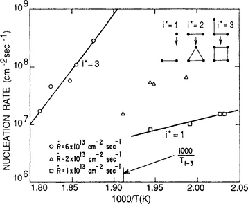
Figure 7-14 Nucleation rate of Ag on (100) NaCl as a function of temperature. Data for three different deposition rates are plotted. Also shown are smallest stable epitaxial clusters corresponding to critical nuclei.
(From Ref. 21.)
A thermally activated nucleation rate whose activation energy is dependent on the size of the critical nucleus is predicted by Eq. 7-37. This suggests the existence of critical temperatures where the nucleus size and orientation may undergo change. For example, the temperature T1→2 at which there is a transition from a one- to a two-atom nucleus is given by equating the respective nucleation rates ![]() . After substitution and some algebra,
. After substitution and some algebra,
or
Use can be made of Eq. 7-38b in analyzing the data shown in Fig. 7-13. The transition of polycrystalline Cu to single-crystal Cu films can be thought of as the onset of (111) epitaxy (i* = 2) from atomic nuclei (i* = 1).
An Arrhenius plot of the line of demarcation between mono- and polycrystal deposits yields an activation energy of Edes+ E2 equal to 1.48 eV. At a deposition rate of 8.5 × 10¹⁴ atoms/cm2-s or 1 Å/s, and n0ν = 6.9 × 1027atoms/cm2 -s, the epitaxial transition temperature is calculated to be 577 K. Equations similar to Eq. 7-38 can be derived for transitions between i* = 1 and i* = 3, or i* = 2 and i* = 3, etc.
It is instructive to compare these estimates of epitaxial growth temperatures with ones based on surface-diffusion considerations (Ref. 22). For the case of smooth layer-by-layer growth on high-symmetry crystal surfaces, adatoms must reach growth ledges by diffusional hopping before other islands nucleate. Atoms must, therefore, migrate a distance of some 100–1000 atoms, the typical terrace width on well-oriented surfaces during the monolayer growth time of ∼ 0.1−1 s. By Eq. 7-30 a surface diffusivity greater than ∼ 10−8 cm2/s is, therefore, required irrespective of the material deposited. This means a different critical epitaxial-growth temperature (TE) depending on whether a semiconductor, metal, or alkali halide films is involved. In the Arrhenius plot of Fig. 7-15, DS values are graphed vs TM/T where TM is the melting point. Similar relationships for lattice, grain-boundary, and dislocation diffusivities will be introduced in Chapter 11. At the critical value of DS = 10−8 cm2/s, Fig. 7-15 indicates that TE ∼ 0.5TM, ∼ 0.3TM, and 0.1TM for layer growth on group IV semiconductors, metals, and alkali halides, respectively. These temperatures agree qualitatively with experimental observations.
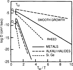
Figure 7-15 Lattice (DL) and surface diffusivities (DS) as a function of TM/T for metals, semiconductors, and alkali halides.
(From Ref. 22.)
7.4.4 KINETIC MODELS OF NUCLEATION
Microscopic approaches to the modeling of nucleation processes have stressed the kinetic behavior of atoms and clusters containing a small number of atoms. Rate equations similar to those describing the kinetics of chemical reactions are used to express the time-dependent change of cluster densities in terms of the processes which occur on the substrate surface. Because these theories and models are complex mathematically as well as physically, the discussion will stress the results without resorting to extensive development of derivations. It is appropriate to start with the fate of the mobile monomers. If coalescence is neglected, then
The equation states that the time rate of change of the monomer density is given by their incidence rate, minus their desorption rate, minus the rate at which two monomers combine to form a dimer. This latter term follows second-order kinetics with a rate constant K1. The last term represents the loss in monomer population due to their capture by larger clusters containing two or more atoms. There are similar equations describing the population of dimer, trimer, etc., clusters as they interact with monomers. The general form of the rate equation for clusters of size i is
where the first term on the right expresses their increase by attachment of monomers to smaller i− 1 sized clusters, and the second term their decrease when they react with monomers to produce larger i+1 sized clusters. There are i of these coupled rate equations to contend with, each one of which is dependent on direct impingement from the vapor as well as desorption through their link back to Eq. 7-35. Inclusion of diffusion terms, i.e., d2Ni/dx2, enables change in cluster shape to be accounted for. When cluster mobility and coalescence are also taken into account, a fairly complete chronology of nucleation events emerges, but at the expense of greatly added complexity.
Transient as well as steady-state (i.e., where dNi dt = 0) solutions have been obtained for the foregoing rate equations for a variety of physical situations and for arbitrary values of i. They typically predict that N(t) increases with time, eventually saturating at the value Ns. In practice the stable nucleus density is observed to increase approximately linearly with deposition time, then saturate at values ranging from ∼ 109 to 1012 cm−2 depending on deposition rate and substrate temperature (Ref. 19). With further deposition N(it) decreases as a result of coalescence. Furthermore, NS is larger the lower the substrate temperature, as shown schematically in Fig. 7-16.
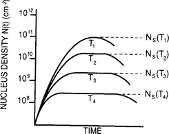
Figure 7-16 Schematic dependence of N(t) with time and substrate temperature. T1>T2>T3>T4.
(From Ref. 19.)
Venables (Ref. 23) has neatly summarized nucleation behavior for cases where iassumes any integer value. In general, the stable cluster density is given by
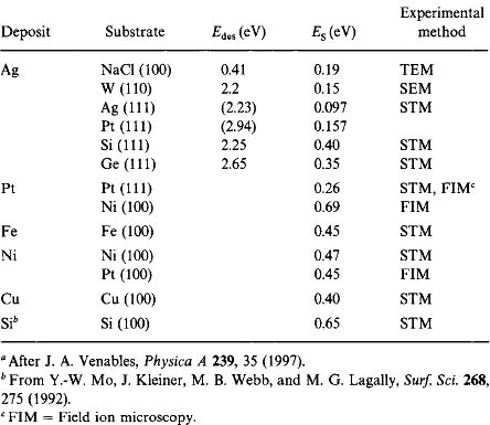
where A is a calculable dimensionless constant dependent on the substrate coverage. As a result of such generalized equations, experimental data for NS have been tested as a function of the substrate temperature and deposition rate. The parameters p and E have respectively yielded values for i* and the energies of desorption, diffusion, and cluster binding. Values for Edes and ES have been extracted for a number of systems, and these are entered in Table 7-1. Because Edes > ES, adatom motion is largely confined to the substrate plane rather than normal to it. Although the major application of the kinetic model has been to island growth, the theory is also capable of describing S-K growth.
7.4.5 CLUSTER COALESCENCE AND DEPLETION
As previously noted, the density of stable nuclei increases with time up to some maximum level before decreasing because of coalescence phenomena. Growth and coalescence of nuclei are generally characterized by the following features:
1. A decrease in the total projected area of nuclei on the substrate occurs.
2. There is an increase in the height of the surviving clusters.
3. Nuclei with well-defined crystallographic facets sometimes become rounded.
4. The composite island generally reassumes a crystallographic shape with time.
5. When two islands of very different orientation coalesce, the final compound cluster assumes the crystallographic orientation of the larger island.
6. The coalescence process frequently appears to be liquid-like with islands merging and undergoing shape changes after the fashion of liquid droplet motion. This is especially true at elevated temperatures.
7. Prior to impact and union, clusters have been observed to migrate over the substrate surface in a process described as cluster-mobility coalescence.
Several mass transport mechanisms have been proposed to account for these coalescence phenomena, and they are discussed in turn.
7.4.5.1 Ostwald Ripening
Prior to coalescence there is a collection of islands of varied size, and with time the larger ones grow or “ripen” at the expense of the smaller ones. The desire to minimize surface free energy of the island structure is the driving force. To understand the process, consider two isolated islands of surface tension y and different size in close proximity as shown in Fig. 7-17a. For simplicity they are assumed to be spherical with radii r1 and r2, and therefore the free energy (G) of a given island is 4πr2iγ (i = 1, 2). The island contains a number of atoms ni given by 4πr3i/3Ω, where Ω is the atomic volume. Defining the free energy per atom μi or chemical potential as dG/dni, after substitution,

Figure 7-17 Coalescence of islands due to (a) Ostwald ripening, (b) sintering, (c) cluster migration.
In chemical thermodynamics the chemical potential is often associated with the so-called “escaping tendency” of atoms. Where μ is large the effective atomic concentration is large, forcing them to escape to where μ is small. This is the case just outside very small particles. Thus, if r1 > r2 as shown, μ2 > μ1, and atoms will diffuse along the substrate from particle 2 (shrinking it in size) to particle 1 which grows at the former’s expense. A mechanism has thus been established for coalescence without the necessity for islands to be in direct contact. In a multi-island array the kinetic details are complicated, but ripening serves to establish a quasi-steady-state island size distribution which changes with time. Ostwald ripening processes never reach equilibrium during film growth, and the theoretically predicted narrow distribution of crystallite sizes is generally not observed.
7.4.5.2 Sintering
Sintering is a coalescence mechanism involving islands in contact. It can be understood by referring to Fig. 7-18, depicting a time sequence of coalescence events between Au particles deposited on molybdenite (MoS2) at 400°C and photographed within the TEM (Ref. 24). Within tenths of a second a neck forms between islands and then successively thickens as atoms are transported into the region. The driving force for neck growth is simply the natural tendency to reduce the total surface energy (or area) of the system. Since the algebraic magnitude of μ for atoms on the convex island surfaces (r > 0) exceeds that for atoms situated in the concave neck (r < 0), an effective concentration gradient between these regions develops.
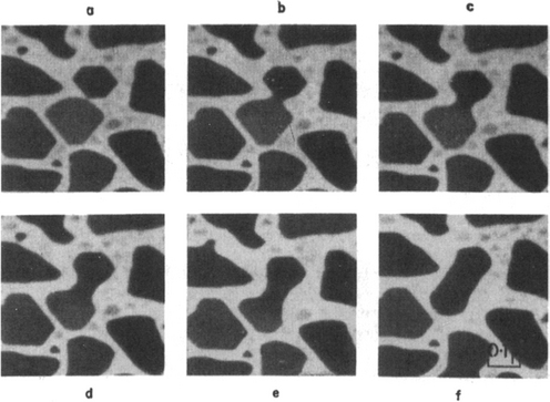
Figure 7-18 Successive electron micrographs of Au deposited on molybdenite at 400°C illustrating island coalescence by sintering. (a) Arbitrary zero time, (b) 0.06 s, (c) 0.18s, (d) 0.50 s, (e) 1.06 s, (f) 6.18 s.
(From Ref. 24.)
This results in the observed mass transport into the neck. Variations in island surface curvature also give rise to local concentration differences that are alleviated by mass flow.
In the case of sintering or coalescence of contacting spheres of radius r (Fig. 7-17b), theoretical calculations in the metallurgical literature (Ref. 25) have shown that the sintering kinetics is given by
Here X is the neck radius, A(T) is a temperature-dependent constant that varies with mass transport mechanism, n and m are constants, and t is the time. Of the several mechanisms available for mass transport in films, the two most likely ones involve diffusion either through the bulk or via the surface of the islands. For bulk diffusion n = 5, m = 2, whereas for surface diffusion n = 7, m = 3. Typical thumbnail calculations show that surface diffusion dominates sintering.
While surface energy and diffusion-controlled mass transport mechanisms undoubtedly influence liquid-like coalescence phenomena, sintering mechanisms are unable to explain the following:
1. Observed liquid-like coalescence of metals on substrates maintained at 77 K where atomic diffusion is expected to cease
2. Widely varying stabilities of irregularly shaped necks, channels, and islands possessing high curvatures at some points
3. The large range of times required to fill visually similar necks and channels
4. Enhanced coalescence in the presence of an applied electric field in the substrate plane
7.4.5.3 Cluster Migration
The last mechanism for coalescence considered deals with migration of clusters on the substrate surface (Fig. 7-17c). Coalescence occurs as a result of collisions between separate island-like crystallites (or droplets) as they execute random motion. Evidence provided by the field ion microscope, which has the capability of resolving individual atoms, has revealed the migration of dimer and trimer clusters. Electron microscopy has shown that crystallites with diameters of ∼ 50–100 Å can migrate as distinct entities provided the substrate temperature is high enough. Interestingly, the mobility of metal particles can be significantly altered in different gas ambients. Not only do the clusters translate, but they have been observed to rotate as well as even jump on each other and sometimes reseparate thereafter! Cluster migration has been directly observed in many systems, e.g., Ag and Au on MoS2, Au and Pd on MgO, and Ag and Pt on graphite in so-called conservative systems, i.e., where the mass of the deposit remains constant because further deposition from the vapor has ceased. Coalescence in a conservative system is characterized by a decreased density of particles, increased mean volume of particles, a particle size distribution which increases in breadth, and a decreased coverage of the substrate.
The surface migration of a cap-shaped cluster with projected radius r occurs with an effective diffusion coefficient D(r) having units of cm2/s. Presently there exist several formulas for the dependence of D on r based on models assumed for cluster migration. The movement of peripheral cluster atoms, the fluctuations of areas and surface energies on different faces of equilibrium-shaped crystallites, and the glide of crystallite clusters aided by dislocation motion are three such models. In each case D(r) is given by an expression of the form (Ref. 26)
where B(T) is a temperature-dependent constant and s is a number ranging from 1 to 3. It comes as no surprise that cluster migration is thermally activated with an energy Ec related to that for surface self-diffusion, and that it is more rapid the smaller the cluster. However, there is a lack of relevant experimental data which can distinguish among the mechanisms. In fact, it is difficult to distinguish cluster mobility coalescence from Ostwald ripening based on observed particle-size distributions.
7.4.5.4 Coalescence and Grain Size
The vocabulary of polycrystalline film formation, particularly terms such as nucleation, growth, and coalescence, has a familiar ring in the metallurgical literature of solid-state phase transformations. For example, a cold-worked metal matrix transforms by nucleation of recrystallized grains (islands) followed by growth, thus consuming the surrounding matrix so that there is less area available for new nuclei. During recrystallization one region will start ahead of others because of some favorable local composition, temperature, defect, or bias in the system. Then nucleation occurs elsewhere, and later somewhere else, while growth continues independently in regions of prior nucleation. The situation is much like rain droplets falling on a pond. Where rain impinges on the pond, surface wave nuclei are created. The circular ripples grow outward and begin to impinge on one another. When all of the prior untransformed matrix disappears by grain growth and impingement or coalescence, recrystallization is complete. So, too, for grain formation during thin-film formation.
An important equation, based on an analysis by Avrami (Ref. 27) more than 60 years ago, is useful in describing the kinetics of such transformations. For the case of film nucleation and growth in two dimensions where circular disklike nuclei grow, the form of the equation is
where f(t) is fractional amount of transformation and t is the time. Furthermore, ![]() (nuclei/cm2-s) and
(nuclei/cm2-s) and ![]() (cm/s) are the nucleation and linear growth rates, respectively. As a function of log t, f(t) is small during what may be thought of as an initial incubation period, then rises sharply when nucleation and growth rates overlap strongly, and finally saturates at f = 1 at long times (see Fig. 11-20a). Suppose when f = 0.95, cluster coalescence is complete and the film is virtually continuous. Substitution shows that the time required, t0.95, is given by the relation
(cm/s) are the nucleation and linear growth rates, respectively. As a function of log t, f(t) is small during what may be thought of as an initial incubation period, then rises sharply when nucleation and growth rates overlap strongly, and finally saturates at f = 1 at long times (see Fig. 11-20a). Suppose when f = 0.95, cluster coalescence is complete and the film is virtually continuous. Substitution shows that the time required, t0.95, is given by the relation ![]() . Provided the nucleation rate is constant, the number of grains nucleated per unit area in this time is
. Provided the nucleation rate is constant, the number of grains nucleated per unit area in this time is ![]() or
or ![]() . If the mean grain diameter is lg, the number of grains per unit area is equivalently (πl2g/4)−1, and therefore by equating terms,
. If the mean grain diameter is lg, the number of grains per unit area is equivalently (πl2g/4)−1, and therefore by equating terms,
That grain size is proportional directly to ![]() and inversely to
and inversely to ![]() is a fundamental idea common to bulk solids (e.g., castings, recrystallized metals) as well as thin films.
is a fundamental idea common to bulk solids (e.g., castings, recrystallized metals) as well as thin films.
In a similar vein, Thompson (Ref. 28), using the Avrami equation, has simulated the processes of cluster nucleation and growth to the point of coalescence. Importantly, connections were drawn between the grain size at cluster impingement and the practical concerns of film stress and texture. The model assumed a substrate consisting of spherical cap clusters as in Fig. 7-11 such that when viewed from above the circular islands were each surrounded by a substrate annular ring of width X populated by adatoms. These diffuse by Eq. 7-30 to enlarge the island rather than form a new nucleus. The resultant film grain size was dependent on X and given by
Provided ![]() Eqs. 7-46 and 7-47 are essentially the same.
Eqs. 7-46 and 7-47 are essentially the same.
It should be noted that the Avrami equation strictly applies to closed systems transforming under conditions where there is no matter exchange with the surroundings. Inclusion of the adatom ring apparently extends the equation’s validity to open systems. An accessible and very readable derivation of the Avrami equation for the three-dimensional case can be found in Tu et al. (Ref. 17); later in Chapter 11 we shall again apply it to phase transformations in thin films.
7.5 EXPERIMENTAL STUDIES OF NUCLEATION AND GROWTH
Assorted microscopic and surface analytical techniques have been employed over the years to reveal the physical processes of nucleation and test the theories that model them. In this section we shall focus on the more important of these experimental methods and the results of illustrative studies.
7.5.1 ELECTRON MICROSCOPY
The traditional tool, particularly for island growth studies, has been the transmission electron microscope (TEM). In this technique metals such as Ag and Au are deposited onto substrates of interest such as cleaved alkali-halide single crystals, e.g., LiF, NaCl, and KCl, in an ultrahigh-vacuum system for a given time at fixed ![]() . The deposit is then covered with carbon and the substrate is dissolved away, leaving a rigid carbon replica which retains the metal clusters in their original crystal orientation. To enhance the very early stages of nucleation the technique of decoration is practiced. Existing clusters are decorated with a lower melting-point metal such as Zn or Cd which does not condense in the absence of prior noble metal deposition. This technique renders visible otherwise invisible clusters which may contain just a few atoms, thus making possible more precise comparisons with theory.
. The deposit is then covered with carbon and the substrate is dissolved away, leaving a rigid carbon replica which retains the metal clusters in their original crystal orientation. To enhance the very early stages of nucleation the technique of decoration is practiced. Existing clusters are decorated with a lower melting-point metal such as Zn or Cd which does not condense in the absence of prior noble metal deposition. This technique renders visible otherwise invisible clusters which may contain just a few atoms, thus making possible more precise comparisons with theory.
A disadvantage of the foregoing postmortem step-by-step observations is that much useful information on intermediate stages of film nucleation and growth is lost. For this reason, in situ techniques within both scanning (SEM) and transmission electron microscopes, modified to contain deposition sources and heated substrates, have been developed, but usually at the expense of decreased resolution. A recent in situ TEM study by Ross (Ref. 29) of the CVD deposition of Ge on Si (001) substrates illustrates the power of such methods. The Ge was grown at 650°C from digermane (Ge2H6) gas at pressures between 10−8 and 10−6 torr while dark-field images were continuously recorded. Epitaxial nucleation was deemed to occur after strain contrast was first detected at a dose of 50 L (or 19 monolayers; see Section 2.2.3) of Ge2H6. Two island shapes–square-bottomed pyramids and steep domes–then grew in a bimodal size distribution. Within minutes at a growth rate of 0.1 to 10 monolayers/min the smaller pyramids disappeared, leaving a sole distribution of dome-shaped islands ∼ 60 nm in size. An Ostwald ripening–like mechanism was suggested to be responsible for the changes in nucleus density. Such observations have enabled a better understanding of the processing of “quantum dot” structures.
7.5.2 AUGER ELECTRON SPECTROSCOPY (AES)
This technique is based on the measurement of the energy and intensity of the Auger electron signal emitted from atoms located within some 5–10 ˚ of a surface that is excited by a beam of incident electrons. The subject of AES will be treated in greater detail in Chapter 10. Here it is sufficient to note that the Auger electron energies are specific to, or characteristic of, the atoms emitting them and thus serve to fingerprint elemental composition. The magnitude of the AES signal is related directly to the abundance of the adatoms in question. Consider now the deposit/substrate combinations corresponding to the three growth modes (Ref. 30). If the AES signal from the film surface of each is continuously monitored during deposition at a constant rate, it will have the coverage or time dependence shown schematically in Fig. 7-19, assuming a sticking coefficient of unity.
Figure 7-19 Schematic Auger signal currents as a function of time for the three growth modes: (a) island, (b) planar, (c) S-K. o = overlayer, s = substrate.
(From Ref. 30.)
In the case of island growth (Fig. 7-19a) the signal from the deposit atoms builds slowly while simultaneously that from the substrate atoms correspondingly falls. The interpretation of the AES signal in the case of layer growth (Fig. 7-19b) is more complicated. During growth of the initial monolayer, the Auger signal is proportional to the deposition rate and sticking coefficient of adatoms, as well as to the elemental detection sensitivity. For the second and succeeding monolayers the sticking coefficients change. This gives rise to slight deviations in slope of the AES signal each time a complete monolayer is deposited, and therefore the overall response is segmented as indicated. For S-K growth (Fig. 7-19c) the signal is ideally characterized by an initial linear increase up to one monolayer or sometimes a few monolayers. Then there is a sharp break and the Auger amplitude rises slowly as islands, covering a relatively small part of the substrate, emerge. It would be misleading to suggest that all AES data fit one of the categories in Fig. 7-19. Complications in interpretation arise from atomic contamination, diffusion and alloying between deposit and substrate, and transitions between two- and three-dimensional growth processes.
7.5.3 SOME RESULTS FOR METAL FILMS
The properties of metal particles and films on nonmetallic substrates have played an important role in optical coating and ceramic bonding technologies, and particularly in the performance and selectivity of catalysts (Ref. 31).
In addition, studies of the nucleation and growth of metals, especially the noble ones, on assorted alkali halide and oxide substrates have long provided the basis for understanding epitaxy and film formation processes. An appreciation of the scope of this past as well as present research activity on metal/substrate systems can be gained by noting that more than 300 references to the research literature refer just to epitaxial Au film/substrate combinations (Ref. 32). Other epitaxial metal-film/substrate systems have been comprehensively tabulated in the earlier literature (Ref. 33) together with deposition methods and variables. The sheer numbers and varieties of metals and substrates involved appears to point to the fact that epitaxy is a rather common phenomenon; island growth is involved in the overwhelming number of studies, but as a caveat the reader should see Sections 8.2.2 and 8.3.5. In the case of Au, epitaxial films have been deposited on metallic, covalent, and ionic substrate. Although the majority of substrate materials have cubic crystal structures, this is not an essential requirement for epitaxy, which occurs, for example, on hexagonal close-packed Zn as well as on monoclinic mica. The fact that epitaxy is possible between materials of different chemical bonding and crystal structure means that its origins are not simple. That a small difference in lattice constants between film and substrate is essential for epitaxy is apparently not true; small lattice mismatch is neither a necessary nor a sufficient condition for epitaxy. The lattice parameter of the metal can either be larger or smaller than that of the substrate. Having said this, it is also true that the defect density in these metal-film “island” epitaxial systems is very much larger than in the “planar” epitaxial semiconductor systems; in these very close lattice matching is maintained.
The following findings, now primarily of historical interest, briefly summarize numerous studies of nucleation and epitaxy of metal films deposited on ionic substrates (Ref. 34).
1. Substrate. The FCC metals generally grow with parallel orientations on (100), (110), and (111) surfaces of NaCl but with the (111) plane parallel to the (100) mica cleavage plane. Complex relative positioning due to translational and, more frequently, rotational movements appears to be the significant variable in epitaxy rather than lattice-parameter differences.
2. Temperature. High substrate temperatures facilitate epitaxy by: (a) lowering supersaturation levels, (b) stimulating desorption of impurities, (c) enhancing surface diffusion of adatoms into equilibrium sites, and (d) promoting island coalescence. The concept of an epitaxial temperature TEhas been advanced for alkali halide substrates. TE depends on both the nature of the substrate and the deposition rate. For example, TE for Ag on LiF, NaCl, KCl, and Kl was determined to be 340, 150, 130, and 80°C, respectively. The progressive decrease in TE correlates with increases in lattice parameter and enhanced ionic polarizabilities, which facilitate attractive forces between metal and substrate atoms.
3. Deposition rate.In general, low deposition rates, ![]() , foster epitaxy. It has been established that epitaxy occurs when
, foster epitaxy. It has been established that epitaxy occurs when ![]() . This inequality is satisfied physically when the rate at which adatoms settle into equilibrium sites exceeds the rate at which adatoms collide with each other. Such an interpretation requires that E be a surface diffusion activation energy rather than Edes + E2 in Eq. 7-38b. The reader should compare this criterion for TEwith those proposed earlier.
. This inequality is satisfied physically when the rate at which adatoms settle into equilibrium sites exceeds the rate at which adatoms collide with each other. Such an interpretation requires that E be a surface diffusion activation energy rather than Edes + E2 in Eq. 7-38b. The reader should compare this criterion for TEwith those proposed earlier.
7.5.4 SCANNING PROBE MICROSCOPY STUDIES OF NUCLEATION
Saved for last, we briefly note several more recent nucleation studies performed with the scanning tunneling (STM) and atomic force microscopes (AFM). These techniques, capable of unprecedented levels of resolution, have dramatically enhanced our understanding of surfaces and the atomic processes that occur on them. In particular, height variations at atomic steps are routinely measured with a resolution of 1 Å by STM. This makes it possible to determine whether islands have grown in only one atomic layer at a time, or atop one another in three dimensions. We start by considering the research by Lagally and co-workers (Refs. 8, 35, 36) on the earliest stages of Si atom homoepitaxy on a (001) Si substrate surface.
7.5.4.1 Silicon on (001) Si
Earlier in Section 7.2.4.1 it was pointed out that the (001) Si surface exhibits a (2 × 1) reconstruction and contains dimer rows. These rotate 90° as successive terraces are accessed giving rise to two types of monatomic steps. When silicon atoms are deposited on such surfaces the new layer of adatom islands form dimer rows. Occasionally, individual adatoms or pairs of atoms are visible. In addition to adatoms there are ad-dimers, which form when two adatoms pair up. Theory and experiment reveal that ad-dimers can translate as well as rotate. Although they exist predominantly on the dimer tops initially, with time they tend to populate the more stable trough configurations between dimers. Deposition on three successive terraces of the surface is shown in Fig. 7-20, each with their adatom island chains (light). Measurement of the island densities from such images recorded at a series of substrate temperatures yields the Arrhenius plot of Fig. 7-21. Because wandering adatoms either find an existing terrace edge or create new islands on the terrace by combining with other adatoms, the density of islands under specified deposition conditions is a measure of the diffusion coefficient. Thus, the energy barrier for surface diffusion determined from Fig. 7-21 is 0.65 eV, the value entered in Table 7-1. Direct STM observation has also revealed strongly anisotropic diffusion of Si adatoms. At 500 K adatom transport is 1000 times faster in the direction parallel to dimer rows than perpendicular to them.
Figure 7-20 Scanning tunneling microscope image of Si deposition on three successive terraces. Field of view is 300 Å × 300 Å.
(From Ref. 35.)

Figure 7-21 Arrhenius plot of island density vs the reciprocal of the substrate temperature.
(From Ref. 35.)
7.5.4.2 Metals on Silicon
In a similar vein, Neddermeyer (Ref. 10) has reviewed studies of the initial stages of metal (Ag, Cu, Pd) film growth on (111) Si substrates. Atoms on this close-packed Si plane undergoes a very complex structural reconstruction that was mentioned in Section 7.2.4.2. In the case of silver, when only one-third of a monolayer deposits on this surface at 90°C, the STM image depicted in Fig. 7-22a is obtained. Individual adatoms of Ag in the form of a ringlike triangular entity denoted by A and B are seen to sit above the otherwise undisturbed substrate atoms. When additional Ag atoms attach to the initial nuclei, the larger faceted clusters C and D form.
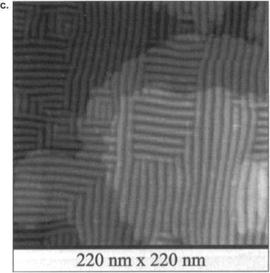
7.5.4.3 Metals on Metals
In a study by Chambliss et al.(Ref. 37) on early stages of metal-film epitaxy, the roles of deposit–substrate strain and place-exchange intermixing were explored by STM. Growth traits of Au, Ag, Ni, and Fe on (111) Au are complicated by a herringbone-like reconstruction of the substrate surface. The latter arises because the smaller number of nearest neighbors on the surface (9) relative to the bulk (12) slightly shortens interatomic spacings so that a 4% greater atomic surface density arises. This means that the reconstructed Au surface is effectively a heteroepitaxial layer lying atop bulk Au. The resultant lattice-mismatch strain creates a complex array of dislocation and stacking fault defects that is manifested in herringbones. A 0.16 monolayer deposit of Ag on (111) Au yields the image shown in Fig. 7-22b. For the most part the Ag deposits are flat and have erased or disrupted the reconstructed Au surface. When the roles of Au and Ag were exchanged, however, it was observed that many Au atoms were buried a few angstroms beneath the (110) Ag substrate surface. This atomic intermixing occurs even at low temperatures. After the surface is covered with such a mixed Au–Ag layer, further Au deposition leads to 3-D Stranski–Krastanov growth of islands.
Interestingly, a similar striped pattern was observed during the electrodeposition of copper on a gold substrate (38). Apparently 10 monolayers of metastable BCC Cu grow pseudomorphically on (100) FCC Au. But a transformation occurs in the 11th layer such that the Cu surface buckles and a new surface structure emerges containing small domains rotated 90° to one another (Fig. 7-22c). This marks the beginning of the deposition of the stable FCC Cu structure.
7.5.4.4 WxN on SiO2
In a last example, let us consider the use of the atomic force microscope (AFM) as a tool in studying film formation of Wx N on amorphous SiO2. The function of this instrument is described in Section 10.3.5.4. Here we simply note that the AFM also traces surface topography, perhaps not with the spatial resolution of the STM, by detecting the van der Waals force interaction between tip and surface. In a study by Li et al.(Ref. 39), nucleation and growth of Wx N films by plasma-enhanced CVD at a deposition temperature of 340°C and rate of 1 nm/s was recorded during the first few seconds. The film topography is shown in Figs. 7-23a, b, c accom panied by information on film chemistry as revealed by Auger spectroscopy (Section 10.4.4). After 1 s there was no detectable W or N Auger signal, so this period may be taken as the deposition incubation time. A Wx N layer formed after 2 s consisting of 320 grains in an area measuring 500 nm × 500 nm, where each grain was ∼ 25 nm in diameter. Cluster coalescence occurred within 3 s, leaving 180 grains within the same area, where the size of each grain was now ∼ 45 nm. Clearly, the lateral grain dimensions are much larger than the nominal film thickness.
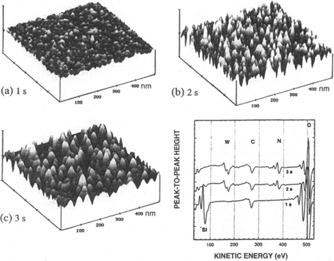
Figure 7-23 Atomic force microscope images of WxN on SiO2 after (a) 1s, (b) 2 s, and (c) 3 s. The respective surface rms roughnesses are 0.13 nm (the same as for the original SiO2), 0.50 nm, and 0.48 nm. Each division represents a length of 100 nm along the horizontal axis and a height of 3 nm on the vertical axis. Corresponding Auger spectra appear in the inset.
(From Ref. 39. Reprinted with the permission of the authors.)
7.6 CONCLUSION
The earliest stages of film formation have long held a fascination for the scientific community. As a result, much direct observation via electron microscopy was carried out over the years to reveal the behavior of small atomic clusters on substrate surfaces. In parallel there was a broad effort to theoretically model film structures and the processes that led to them, even though individual atoms could not be directly resolved. However, these traditional studies have been dramatically augmented in recent years by scanning probe techniques, particularly scanning tunneling microscopy, possessing the power to directly image adatom motion during deposition. In this way the crystallographic and kinetic details of nucleation events in a number of film/substrate systems, particularly semiconductor/semiconductor, but also metal/semiconductor as well as metal/ceramic, have been exposed.
The bulk of this chapter has been devoted to modeling nucleation ![]() and growth
and growth ![]() rates in terms of classical thermodynamic and kinetic descriptions, adopting both macroscopic and microscopic points of view. Starting with concepts of surface tension and capillarity theory, equilibrium sizes of nuclei and the energies to form them were thermodynamically estimated. Upon incorporating atomic surface-diffusion effects while allowing for loss of adatoms due to desorption, estimates for the macroscopic nucleation rate were obtained in terms of deposition variables and the materials properties involved. Atomistic theories have similarly yielded analogous expressions for nucleation rates. Theoretical modeling of nucleation and growth phenomena has aided our understanding of issues related to thin-film grain size and epitaxy. For example, in the former case large grains are fostered at high substrate temperatures, where
rates in terms of classical thermodynamic and kinetic descriptions, adopting both macroscopic and microscopic points of view. Starting with concepts of surface tension and capillarity theory, equilibrium sizes of nuclei and the energies to form them were thermodynamically estimated. Upon incorporating atomic surface-diffusion effects while allowing for loss of adatoms due to desorption, estimates for the macroscopic nucleation rate were obtained in terms of deposition variables and the materials properties involved. Atomistic theories have similarly yielded analogous expressions for nucleation rates. Theoretical modeling of nucleation and growth phenomena has aided our understanding of issues related to thin-film grain size and epitaxy. For example, in the former case large grains are fostered at high substrate temperatures, where ![]() is large, and at low deposition rates, where
is large, and at low deposition rates, where ![]() is small. Both trends are consistently incorporated into a quantitative relationship which predicts that film grain size ought to vary as
is small. Both trends are consistently incorporated into a quantitative relationship which predicts that film grain size ought to vary as ![]() .
.
Exercising practical control over thin-film structures means integrating an understanding of the detailed atomistic processes on real surfaces with the macroscopic implications of nucleation and growth theories.
1. Among the surface electronic properties affected by differences in work function are thermionic emission and photoemission. The defining equations for these phenomena are j = AT2 exp –(qφ/kBT) and KE = hv − q φ, respectively. Here jis the thermionic current density, Ais a constant, T is the temperature, q is the electronic charge,KE is the photoelectron kinetic energy, h is Planck’s constant, and ν is the frequency of the incident light. By alloying the surface of tungsten with cesium it is found that φ is reduced from 4.5 to 1.4 eV.
2. An adatom overlayer structure on a close-packed substrate surface, e.g., the (111) plane where atoms have hexagonal symmetry, is defined as (31/2 × 31/2)R 30°. Sketch probable substrate and adatom positions for this case.
3. Consider a (110) substrate mesh containing adatoms lying along [001] and ![]() directions.
directions.
Sketch the substrate and adatom positions for both cases.
4. Just as it is thermodynamically impossible to produce a perfectly pure material, explain why it is thermodynamically impossible to produce zero coverage (θ = 0) or unity coverage (θ = 1) adatom surface layers.
Hint:Evaluate d(G/ns)/dθ at θ = 0 and 1.
5. A gas molecule with initial energy Ei approaches a surface.
7. A cylindrical pill-like cluster of radius r nucleates on a dislocation that emerges from the substrate. The free-energy change per unit thickness is given by
where A − B ln rrepresents the dislocation energy within the cluster.
8. During e-beam evaporation, suppose that small metal particles (several nanometers in diameter) deposit on a substrate consisting of a metal covered with a thin dielectric oxide film. The particles are found to be charged so that a capacitor-like structure is formed.
9. Young’s equation plays a role in soldering technology.
10. Cap-shaped nuclei on substrates grow both by direct impingement of atoms from the vapor phase and by attachment of adatoms diffusing across the substrate surface.
12. Two spherical nuclei of radii r1 and r2 are separated by a distance L. If r1 ![]() r2, derive an expression for the time it will take for the smaller nucleus to disappear by sequential atomic dissolution and diffusion to the larger nucleus by Ostwald ripening. Assume that the diffusivity of atoms on the surface is Ds. Make simplifying assumptions as you see fit.
r2, derive an expression for the time it will take for the smaller nucleus to disappear by sequential atomic dissolution and diffusion to the larger nucleus by Ostwald ripening. Assume that the diffusivity of atoms on the surface is Ds. Make simplifying assumptions as you see fit.
13. Assume that the two nuclei in Fig. 7-18 coalesce by a sintering mechanism.
14. A film is deposited on a substrate by means of evaporation. In the expression for the rate of heterogeneous nucleation (Eq. 7-33), identify which terms are primarily affected by:
In each case qualitatively describe the nature of the change.
15. An atomic force microscope study of the nucleation and growth of polycrystalline silicon on SiO2 substrates by rapid-thermal CVD methods revealed the following:

16. A number of years ago a commercial product was introduced that enabled a metal to deposit only in a selected masked area of a substrate and nowhere else. In operation, a porous metal pellet containing a proprietary ingredient was heated to a high temperature where a colorless substance presumably coated all surfaces within the chamber except that which was masked. Then the mask was removed from the substrate and the desired metal was evaporated. A thin metal film only deposited on the substrate surface previously masked. Remarkably, the area deposited on did not have to be in the line of sight of the evaporated metal source. Propose a scenario that would scientifically explain this apparently magical behavior.
1 Lewis B., Anderson J.C. Nucleation and Growth of Thin Films. London: Academic Press; 1978.
2 Vook R.W. Int. Metals Rev.. 1982;27:209.
3 Duke C.B., editor. Surface Science: The First Thirty Years, Surf. Sci. 1994;299/300.
4 Harrison W.A. Solid State Theory. New York: McGraw-Hill; 1970.
5 Prutton M. Introduction to Surface Physics. Oxford: Clarendon Press; 1994.
6 Wert C.A., Thomson R.M. Physics of Solids, 2nd ed. New York: McGraw-Hill, 1970.
7 Woodruff D.P., Delchar T.A. Modern Techniques of Surface Science. 1997.
8 Zhang Z., Wu F., Lagally M.G. Ann. Rev. Mater. Sci.. 1997;27:525.
9 Farnsworth H.E., Shlier R.E., Dillon J.A. J. Chem. Phys. Solids. 1959;8:116.
10 Neddermeyer H. Crit. Rev. Solid State Mater. Sci.. 1990;16(5):309.
11 Kubby J.A., Boland J.J. Surf. Sci. Rep.. 1996;26:21.
12 Ertl G., Freund H.J. Physics Today. 1999;52(1):32.
13 Konuma M. Film Deposition by Plasma Techniques. Berlin: Springer Verlag; 1992.
14 Cottrell A.H. Theoretical Structural Metallurgy. London: Edward Arnold; 1948.
15 Jackson K., Uhlmann D., Hunt J. Crystal Growth. 1967;1:1.
16 Tsao J.Y. Materials Fundamentals of Molecular Beam Epitaxy. Boston: Academic Press; 1993.
17 Tu K.-N., Mayer J.W., Feldman L.C. Electronic Thin Film Science for Electrical Engineers and Materials Scientists. New York: Macmillan; 1992.
18 Neugebauer C.A. Maissel L.I., Glang R. Handbook of Thin-Film Technology. New York: McGraw-Hill, 1970.
19 Reichelt K. Vacuum. 1988;38:1083.
20 Wessels B.W. J. Vac. Sci. Technol.. 1997;B(15):1056.
21 Walton D., Rhodin T.N., Rollins R.W. J. Chem. Phys.. 1963;38:2698.
22 Yang H.M., Flynn C.P. Phys. Rev. Lett.. 1989;62:2476.
23 Venables J.A. Surf. Sci.. 1994;299/300:798.
24 Pashley D.W., Stowell M.J. J. Vac. Sci. Technol.. 1966;3:156.
25 German R.M. Powder Metallurgy Science. Princeton, NJ: Metal Powder Industries Federation; 1984.
26 Kashchiev D. Surf. Sci.. 1979;86:14.
27 Avrami M., J. Chem. Phys. 1937;7:1103. Avrami M., J. Chem. Phys. 1940;8:212. Avrami M. J. Chem. Phys.. 1941;9:177.
28 Thomspon C.V. J. Mater. Res.. 1999;14:3164.
29 Ross F.M. IBM J. Res. Develop.. 2000;44:489.
30 Rhead G.E. J. Vac. Sci. Technol.. 1976;13:603.
31 Dufour L.-C., Perdereau M. Dufour L.-C., Monty C., Petot-Ervas G. Surfaces and Interfaces of Ceramic Materials. The Netherlands: Kluwer, Dordrecht, 1989.
32 Vook R.W., Oral B. Gold Bull.. 1987;20(1/2):13.
33 Grunbaum E. Matthews J.W., editor. Epitaxial Growth B. New York: Academic Press, 1976.
34 Chopra K.L. Thin-Film Phenomena. New York: McGraw-Hill; 1969.
35 Lagally M.G. Physics Today. 1993;46(11):24.
36 Mo Y.-W., Kleiner J., Webb M.B., Lagally M.G. Surf. Sci.. 1992;268:275.
37 Chambliss D.D., Wilson R.J., Chiang S. IBM J. Res. Develop.. 1995;39:639.
38 Randier R.J., Dietterle M., Kolb D.M. Z. Phys. Chem.. 1999;208:43.
39 Li H., Jin S., Bender H., Lanckmans F., Heyvaert I., Maex K., Froyen L. J. Vac. Sci. Technol.. 2000;B18(l):242.