
Chapter 10 Characterization of Thin Films and Surfaces
10.1 INTRODUCTION
Scientific disciplines are identified and differentiated by the experimental equipment and measurement techniques they employ. The same is true of thin-film science and technology. For the first half of this century interest in thin films centered on optical applications. The role played by films was largely a utilitarian one necessitating measurement of film thickness and optical properties. At first single films on thick substrates were involved. However, with the explosive growth of thin-film utilization in microelectronics there was an important need to understand the intrinsic nature of films in more complex materials environments. Increasingly, the benefits of multilayer film structures have been realized in an assortment of high-technology applications. Examples include multilayer metal and insulating films in microelectronics, compound semiconductor films in optoelectronics, dielectric-film stacks for optical coatings, and ceramic film layers in hard coatings.
With the increasingly interdisciplinary nature of applications, new demands for film characterization and property measurements in both individual films and multilayer coatings have arisen. It was this necessity that drove the creativity and inventiveness that culminated in the development of an impressive array of commercial analytical instruments. These are now ubiquitous in the thin-film, coating, and broader scientific communities. In many instances it was a question of borrowing and adapting existing techniques employed in the study of bulk materials (e.g., X-ray diffraction, microscopy, mechanical testing) to meet the challenges posed by thin-film applications. In other cases well-known physical phenomena (e.g., electron spectroscopy, nuclear scattering, mass spectroscopy) were exploited.
A partial list of the modern techniques employed in the characterization of thin-film materials and devices appears in Table 10-1 (Ref. 1). Among their characteristics are the unprecedented structural resolution and chemical analysis capabilities over both small lateral and depth dimensions. Some techniques only sense and provide information on the first few atom layers of the surface. Others probe more deeply but in most cases depths of a micron or less are analyzed. Virtually all of these techniques require a high- or ultrahigh-vacuum ambient. Some are nondestructive while others are not. All of them utilize incident electron, or ion, or photon beams. These interact with the surface and excite it in such a way that some combination of secondary beams of electrons, ions, or photons are emitted, carrying off valuable structural and chemical information in the process. A rich collection of acronyms–a savory alphabet soup– has emerged to differentiate the various techniques. These abbreviations now widely pervade the thin-film and surface-science literature.

General testing and analysis of thin films is carried out with equipment and instruments that are wonderfully diverse in character. For example, consider the following extremes in their attributes:
1. Size. This varies from a portable desktop interferometer to the 50-foot long accelerator and beam line of a Rutherford backscattering (RBS) facility.
2. Cost. There is a wide variation in cost from the modest levels for test instruments required to measure electrical resistivity of films, to the near million-dollar price tag of an Auger spectrometer.
3. Operating environment. This varies from the ambient in the measurement of film thickness to the 10−10 torr vacuum required for the measurement of film-surface composition.
4. Sophistication. At one extreme is the manual Scotch-tape film peel-test to evaluate adhesion; at the other is an assortment of electron microscopes and surface analytical equipment where operation, data gathering, display, and analysis are computer controlled.
What is remarkable is that films can be characterized structurally, chemically, and with respect to various properties with almost the same ease and precision that we associate with bulk measurements. This despite the fact that there are many orders of magnitude fewer atoms available in films. To appreciate this, consider AES analysis of a Si wafer surface layer containing 1 at.% of an impurity. Only the top ∼ 15 Å is sampled and since state-of-the-art systems have a lateral resolution of 500 Å, the total measurement volume corresponds to ![]() (500)2 15 = 3 × 10⁶ Å3. In Si this corresponds to about 150,000 matrix atoms and therefore only 1500 impurity atoms are detected in the analysis! Such measurements pose challenges in handling and experimental techniques but the problems are usually not insurmountable.
(500)2 15 = 3 × 10⁶ Å3. In Si this corresponds to about 150,000 matrix atoms and therefore only 1500 impurity atoms are detected in the analysis! Such measurements pose challenges in handling and experimental techniques but the problems are usually not insurmountable.
This chapter will only address, with roughly equal coverage, the experimental techniques and applications associated with determination of:
These represent the common core of information required of all films and multilayer coatings irrespective of ultimate application. Within each of these three categories only the most important techniques will be discussed. Beyond these characteristics there are a host of individual properties (e.g., hardness, adhesion, stress, electrical conductivity) which are specific to the particular application. Measurement techniques for specific properties will therefore be addressed in the appropriate context within the book.
10.2 FILM THICKNESS
10.2.1 INTRODUCTION
Thickness of a film is among the first quoted attributes of its nature. The reason is that thin-film properties usually depend on thickness. Historically the use of films in optical applications spurred the development of techniques capable of measuring film thicknesses with high accuracy. In contrast, other important film characteristics, such as structure and chemical composition, were only characterized in the most rudimentary way until relatively recently. The actual film thickness, within broad limits, is not particularly crucial to function in some applications. Decorative, metallurgical, and protective films and coatings are examples where this is so. On the other hand, microelectronic applications generally require the maintenance of precise and reproducible film metrology, i.e., thickness as well as lateral dimensions. Even more stringent thickness requirements must be adhered to in multilayer optical-coating applications.
The varied types of films and their uses have generated a multitude of ways to measure film thickness. They are basically divided into optical and mechanical methods, and are usually nondestructive but sometimes destructive in nature. In the overwhelming majority of techniques convenience requires that films be removed from the deposition chamber for measurement. However, a number of methods are either commercially available or can be experimentally adapted for real-time monitoring of film thickness during growth. We start with the theory and practice of optical techniques, subjects that are extensively treated in many books and references on thin films (Refs. 2-4).
10.2.2 OPTICAL METHODS FOR MEASURING FILM THICKNESS
Optical techniques for film-thickness determinations are widely used because they are applicable to both opaque and transparent films and generally yield thickness values of high accuracy. In addition, measurements are rapidly performed, frequently nondestructive, and utilize relatively inexpensive equipment. A list of optical techniques devised to measure the thickness and related optical properties of thin films is given in Table 10-2 together with relevant details. The first five are traditional methods that are essentially limited to measuring the thickness of a single film layer on a substrate. In recent years newer techniques such as spectral reflectometry and spectroscopic ellipsometry have supplanted these older methods. The principles of physical optics on which they are based have, of course, not changed in the interim. Capitalizing on advances in spectroscopy instrumentation, coupled with computer control and powerful computational analysis capabilities, these newer instruments have revolutionized the metrology of thin films. Importantly, they are now extensively used in integrated-circuit production environments to characterize multilayer film processing.
Table 10-2 Optical Techniques for Measuring Film Thickness
| Method | Range (nm) | Characteristicsa |
|---|---|---|
| 1. Multiple beam interferometry (FET) | 3–2000 ± 1–3 | A step and reflective coating required (1λ, θ = 90°) |
| 2. Multiple beam interferometry (FECO) | 1–2000 ± 0.5 | A step, reflective coating, and spectrometer required; time consuming (Mλ) |
| 3. VAMFO | 80–1000 ± 0.02–0.05% | Transparent films on reflective substrate (1×, M8) |
| 4. CARIS | 40–2000 ± 1 nm | Transparent films on reflective substrate (Mλ, θ = 90°) |
| 5. Ellipsometry | <0.1– | Transparent films and multilayers, uses polarized light, measures d, n, and k (1λ, fixed θ) |
| 6. Spectral reflectometry (unpolarized) | ∼30–2000 ± 1 nm | Transparent films and multilayers, fast, measures d, n, and k (λ=˜ 200–1000 nm, θ = 90°) (polarized reflectometry is also performed at 1λ, Mθ) |
| 7. Spectroscopic ellipsometry | < 0.1 – | Transparent films and multilayers, uses polarized light (Mλ, fixed θ) (multiple-angle ellipsometry is also performed at 1λ) |
a M = multiple, i.e., wavelengths (λ) or angles (θ).
Interferometry and ellipsometry are the two basic optical methods for determining film thickness. In both, incident light impinges on the film surface and a reflected portion is measured. Interferometry relies on the interference of two or more beams of light, e.g., from the air/film surface and film/substrate interfaces, where the optical path difference is related to film thickness. Light generally impinges normal to the film surface and the instrumentation differs depending on whether opaque or transparent films are involved. Ellipsometry is not an interferometric technique. Rather, changes in the state of polarization of light reflected from surfaces at nonnormal incidence is measured.
The more data an experimental technique provides, the greater are the parameters it can measure with confidence. We shall see the truth of this in the progressive increase of information content in the optical techniques considered, first for thickness determinations in single films, and then in multifilm layers.
10.2.3 INTERFEROMETRY
10.2.3.1 Opaque Films
For opaque films a sharp step down to the substrate plane must be first generated either during deposition through a mask or by subsequent etching. A neighboring pair of light rays reflected from the film/substrate will travel different lengths and interfere by an amount dependent on the step height. To capitalize on the effect, multiple beam interferometry, a technique developed by Tolansky (Ref. 5), is employed. This requires that the optical reflectance of both the film and substrate be very high as well as uniform. A metal such as Al or, better yet, Ag is evaporated over both film and substrate for this purpose. Interference fringes are generated by placing a highly reflective, but semitransparent, optically flat reference plate very close to the film-step-substrate region as shown in Fig. 10-1a. The two highly reflective surfaces are tilted lightly off-parallel enabling the light beam to be reflected in a zigzag fashion between them many times. A series of increasingly attenuated beams are now available for interference. This sharpens the resultant, so-called Fizeau fringes of equal thickness which can be viewed with a microscope.
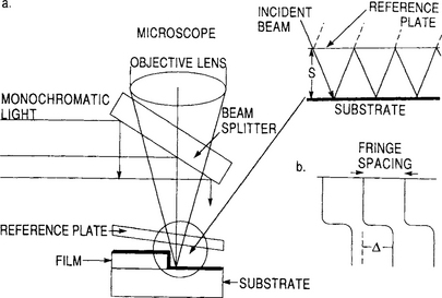
Figure 10-1 (a) Schematic view of experimental arrangement required to produce multiplebeam Fizeau fringes. (b) Fringe displacement at step.
The condition for constructive interference is that the optical path difference between successive beams be an integral number of wavelengths or
Here S is the distance between film and flat, λ is the wavelength of the monochromatic radiation employed, and j is an integer. The phase change accompanying reflection, δ, is assumed to be the same at both surfaces and is taken to be π because of the high film reflectances. Therefore,
and the distance between maxima of successive fringes corresponds to S = λ/2. The existence of the step now displaces the fringe pattern abruptly by an amount Δ (Fig. 10-1b) proportional to the film thickness given by
For highly reflective surfaces, the fringe width is about ∼ 1/40 of the fringe spacing. Displacements of about ∼ 1/5 of a fringe width can be detected. For the Hg green line (λ = 5640 Å) the resolution is therefore (1/40)(1/5)(5640/2) = 15 Å. The resolution and ease of measurement are, respectively, influenced by the fraction of incident light reflected (R) and the fraction absorbed (A) by the film overlying the step. Raising R from 0.9 to 0.95 reduces the fringe width by half, whereas high A values reduce the fringe intensity.
The technique we have just described relies on fringes of equal thickness (FET). Fringes of equal chromatic order (FECO) form the basis of another optical method for measuring the thickness of opaque films (Ref. 2).A similar reflective surface and step are required, but white, rather than monochromatic, light is employed. Instead of a microscope the reflected light is spectrally analyzed by a spectrometer. Film thicknesses ranging from 1 to 2000 nm can be measured with an error of ± 5 Å.
10.2.3.2 Transparent Films
A perfectly suitable method for measuring the thickness of a transparent film is to first generate a step, metallize the film/substrate, and then proceed with either the FET or FECO techniques just discussed. However, transparent films are ideally suited for interferometry because interference of light occurs naturally between beams reflected from the two film surfaces. This means that a step is no longer required. Since different interfaces (the air/film and film/substrate) are involved for the beams that interfere, precautions must be taken to account for phase changes on reflection. Importantly, Fig. 10-2 summarizes what happens when monochromatic light of wavelength λ is normally incident on a transparent film/substrate combination. If n1 and n2 are the respective film and substrate indices of refraction, the intensity of the reflected light undergoes oscillations as a function of the optical film thickness or n1d. When n1 > n2, the maxima occur at film thicknesses equal to
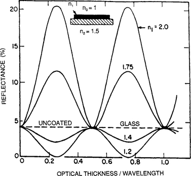
Figure 10-2 Calculated variation of reflectance (on air side) with normalized thickness (n2 d/λ) for films of various refractive indices on a glass substrate of index 1.5.
(From Ref. 3.)
For values of d halfway between these, the reflected intensity is minimum. When n1 < n2, a reversal in intensity occurs at the same optical film thickness. In Fig. 10-2 these results are shown for the case of a glass substrate (n = 1.5) and for films in which n1 is either greater or less than 1.5. In order to exploit Fig. 10-2 for the measurement of film thickness, it is necessary to devise experimental arrangements so that the light-intensity oscillations can be revealed. Two of the techniques, VAMFO and CARIS, now primarily of historical interest (Ref. 2), have a useful pedagogical value.
In VAMFO (variable-angle monochromatic fringe observation) provision is made to vary the incident angle of monochromatic light on the film. As the stage and sample are rotated, bright (maxima) and dark (minima) fringes are observed on the film surface as the optical path changes. For the case of a transparent film on an absorbing reflecting substrate the film thickness is simply given by
where θ is the angle of refraction in the film, and N0 is the fringe order, which is measured by counting successive minima starting from perpendicular incidence. More accurate d values are obtained when the easier-to-detect intensity minima are measured (N0 = ![]() etc.). A disadvantage of VAMFO is that the refractive index of the film must be known at the wavelength of measurement. At best, film thicknesses ranging between 800 and 10,000 Å can be measured with a precision of 0.02 to 0.05%.
etc.). A disadvantage of VAMFO is that the refractive index of the film must be known at the wavelength of measurement. At best, film thicknesses ranging between 800 and 10,000 Å can be measured with a precision of 0.02 to 0.05%.
As FECO is to FET, so CARIS (constant-angle reflection interference spectroscopy) is to VAMFO. In CARIS, the wavelength of the incident light rather than the angle of observation is systematically varied. Light is reflected from the film into a spectrometer with fringes being formed as a function of wavelength. For homogeneous films, the thickness (400-20,000 Å with 10 Å or 0.1% precision) is determined by measuring the number of fringes between two specified wavelengths.
10.2.3.3 Step Gauges
If there is a particular need to roughly estimate the thickness of one kind of film, it may be advantageous to construct a step gauge. Films of different but independently known thickness are deposited on the substrate of interest and are arrayed sequentially. Interference colors, observed when the specimen film is examined in reflected light, are matched to the color of the step gauge standard. For example, a step gauge for SiO2 films on a Si wafer has proven to be useful in estimating film thickness to approximately 200 Å. To use such a gauge the spectral order must be known. In fluorescent light, for example, successive green-yellow colored oxides reappear at ∼ 2000 Å intervals. An SiO2 step gauge can be simply prepared by etching an oxidized Si wafer into a wedge shape by slowly lifting it from a dilute HF etchant in which it is immersed, at a constant velocity.
10.2.3.4 Spectral Reflectometry
Everything considered thus far with respect to interferometry has dealt with a single film on a thick substrate. Secondly, it has been assumed that the films are transparent so that light propagates without absorption. Therefore, the reflected intensity simply depends only on the index of refraction, n. But as noted earlier, multilayer film stacks are increasingly important. In the case of integrated circuits, dielectric and semiconductor layered stacks containing films such as SiO2, silicon nitride, polysilicon, and photoresist on assorted substrates must be routinely characterized in production settings. Furthermore, all largely "transparent" films do absorb some light. Film-thickness measurement systems based on spectral reflectivity are currently employed to overcome the difficulties posed in measuring multiple, partially absorbing layers. In these systems a broad spectral range of wavelengths is employed to increase the information content required. This additional capability is needed because the films have wavelength-dependent optical properties.
To treat these complications we start by defining the complex index of refraction N, where
This form of N reflects an admixture of the ability of materials to both transmit (n) light at a speed of c/n (c = speed of light in vacuum) as well as partially absorb (k) it. The imaginary component k, known as the absorption or extinction coefficient, is a measure of the latter attribute. Its influence on reflectivity (R) of light from a surface can be appreciated if we recall from elementary physics that during normal incidence
if there is no absorption. However, when k is nonzero,
When films are present these formulas are more complex because of multiple reflections at internal interfaces, and the fact that n and k are both wavelength (λ) dependent. Unlike the simple case of Fig. 10-2, this causes the reflectivity of multilayer film stacks to undergo complex oscillations of variable periodicity and amplitude versus λ. An example of the reflectivity response is shown in Fig. 10-3a for a 442.8 nm thick film of Nb2O5 on fused silica.
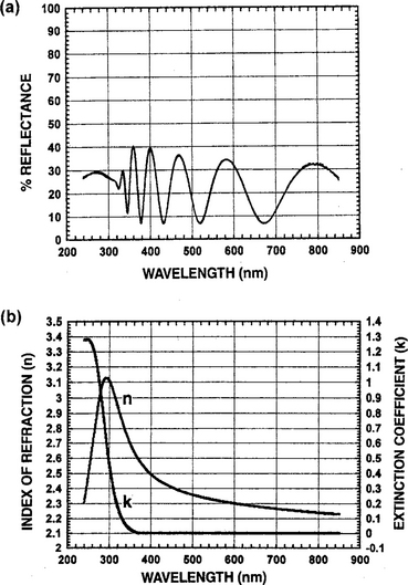
Figure 10-3 (a) Reflectivity vs wavelength for 442.8-nm thick Nb2O5 film on fused silica. (b) n and k vs wavelength for Nb2O5.
(Reprinted with the permission of Scientific Computer International.)
What spectral reflectance methods attempt to do is extract values of film thickness (d), n, and k from the measurement of the normally reflected light intensity over a broad wavelength range. In working backward, this normal-incidence interferometry analysis first makes use of physical connections between n and k known as the Kramers–Kronig relations (Ref. 6); these enable n and k to be self-consistently determined. Then powerful desktop computer analysis uses these derived values of n and k to simulate a predicted R-λ dependence that is matched to the measured R-λ response. Values for d, n, and k are then reported for the iteration that yields the best "goodness of fit" to the data. The technique illustrated in Fig. 10-4 is quite simple experimentally and makes no use of microscopes, optical flats, or angular tilting of specimens, but rather fiber-optic spectrophotometry instead.
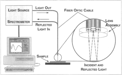
Figure 10-4 Experimental arrangement for spectral reflectivity. Light impinges on the film surface through the central optical fiber of the lens assembly. The reflected light signal is collected by the outer six fibers and analyzed by the spectrometer. A sophisticated program extracts film thickness and optical constants from the computed reflectivity that most closely matches the measured reflectivity data.
(Courtesy of Filmetrics, Inc.)
Key to the success of these methods is the assumptions made for n and k. Nonabsorbing films (k = 0) are usually modeled by the Cauchy approximation, i.e., n(λ) = a + b/λ2 + c/λ4 where a, b, and c are fitting parameters. Similarly, k(λ) = a’ exp b’(1λ– 1/c’), with a’, b’, and c’ fitting parameters, is sometimes used to model the absorption coefficient. For partially absorbing films, a set of energy (E = hc/λ)-dependent n and k values appropriate for a wide variety of semiconductors and dielectrics spanning the ultraviolet to the near infrared has the form (Refs. 7, 8)
Parameters Ai, Bi, and Ci are related to the electronic structure of the material; Eg is the energy bandgap; and B0i and C0i depend on these four previous quantities. The integer q specifies the number of terms to be used in the sum. Term q = 1 describes spectra from an amorphous structure while higher-order terms q ≥ 2 arise from polycrystalline or crystalline material. Each term in the sum for n(E) and k(E) contributes either a peak or a shoulder to the respective spectra. The details of the calculation are complicated and well beyond the scope of this book. Results obtained for n(λ) and k(λ) in Nb2O5 are shown in Fig. 10-3b.
10.2.4 ELLIPSOMETRY
10.2.4.1 Introduction
Also known as polarimetry and polarization spectroscopy, the technique of ellipsometry is over a century old and associated with prominent scientists such as Brewster, Fresnel, Lord Rayleigh, and Drude (Ref. 9). Long used to obtain the thickness and optical constants of dielectric films, ellipsometry is now the preferred way to measure the optical properties of films and multilayer dielectric-film stacks. And as we shall see, it also possesses the capability of monitoring films in situ during deposition and processing (Refs. 10, 11). Because of its sensitivity in the submonolayer (sub-angstrom) thickness range and ability to function at high temperatures or pressures, through gases and liquids, etc., ellipsometry has been incorporated into plasma and CVD reactors, and MBE equipment, as well as electrochemical cells.
Ellipsometry consists of measuring and interpreting the change of polarization state that occurs when a polarized light beam is reflected at nonnormal incidence from a film surface. Since ellipsometry does not rely on interference effects, film thickness determinations are not limited by the wavelength of light. Two variants of ellipsometry have gained great currency, namely multiple-angle-of-incidence and multiple-wavelength or spectroscopic ellipsometry. These will be briefly treated after some basics are presented and standard reflection ellipsometry is described.
10.2.4.2 Polarized Light and Its Interaction with Surfaces
Electromagnetic waves are transverse in nature consisting of mutually perpendicular electric and magnetic field vectors that are also perpendicular to the wave propagation direction. Only the electric-field vector ε is pertinent to our discussion. Consider now a monochromatic light wave propagating in the plane of the page with two sinusoidally-oscillating components of ℰ, one parallel (ℰp) to, and the other (ℰs) perpendicular to the page plane. If these two sinusoidal field components of the same wavelength are in phase they add to yield plane-polarized light, but if they are out of phase elliptically polarized light emerges. As a special case, if the maximum of one coincides with the minimum of the other, the phase difference is 90° and we speak of circularly polarized light. Interestingly, when plane-polarized light reflects from a metal surface both components generally undergo different phase shifts and the emergent light is elliptically polarized.
In Fig. 10-5 plane-polarized light emanating from a medium whose refractive index is n0 is incident on a bare surface of refractive index n1. Angles of incidence (ϕ1) reflection (ϕ1) and refraction (ϕ2), all measured relative to the surface normal, lie in and define the plane of incidence. Light rays in this plane consist of the transverse oscillating electric field components described above. Interaction with the surface causes both the phase and the amplitude of the reflected light (r) components to change, and relative to the incident (i) light it is both elliptically polarized and attenuated as shown. This contrasts with the case of light normally incident on a film/substrate combination where the distinction between parallel and perpendicular polarizations vanishes. Now, however, the two components of reflectivity, rp and rs, are distinct (Ref. 12). The ratio of their amplitudes, equal to a complex reflection coefficient (ρ), yields the fundamental equation of ellipsometry,
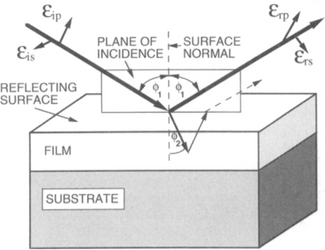
Figure 10-5 Reflection of a light beam from a surface. Refraction, reflection, and polarization effects are shown.
This means two quantities, tan ψ and Δ, must be measured; the former is related to the amplitude ratio, while Δ is the phase difference that develops between the s and p field components after reflection. A similar but more complex equation holds when a film is present on the substrate. Now Δand ψ depend on λ, ϕ1, and five material parameters, i.e., complex refractive indices (n and k) for both the film and substrate, and of course the film thickness. The objective is to extract either the film thickness, or alternatively, the film index of refraction, a task generally requiring computer analysis.
10.2.4.3 Reflection Ellipsometry
The experimental arrangement for standard single-wavelength ellipso-meter measurements is shown in Fig. 10-6. First, the light source, which is normally a laser, is linearly polarized with a polarizer. Upon passing through a quarter-wave plate (compensator) the two field components emerge 90° out of phase so the light is circularly polarized. After impingement on the specimen surface the reflected light, now linearly polarized, is transmitted through a second polarizer which serves as the analyzer. The light intensity is monitored with a photomultiplier detector. Rotation of the polarizer and analyzer until a null or light extinction occurs enables Δand ψ to be determined.

Figure 10-6 Experimental arrangement in ellipsometry. In null ellipsometry a quarter-wave plate is held in a fixed position prior to reflection. The polarizer and analyzer are rotated to obtain the null.
(From Ref. 12. Copyright © 1993 by Academic Press, Inc. Reprinted with the permission of the publishers.)
Data analysis is reasonably straightforward for smooth homogeneous films, but complications arise when the films are inhomogeneous, contain a phase mixture, or have rough surfaces and/or interfaces. For example, surface roughness can be modeled as a film containing voids. In general, an optical response is computed from assumed models of the film structure and compared to experimental data using regression analysis to yield the desired parameters.
10.2.4.4 Multiple-Angle-of-Incidence Ellipsometry
When more independent measurements are required to determine the optical constants (n, k) of the film/substrate or multilayer-film/substrate and film thickness(es), one option is to employ multiple-angle-of-incidence (MAI) ellipsometry. This entails measuring Δand ψ at a number of different ϕ1 values. Among the advantages of MAI is the removal of order ambiguity when measuring the thickness of thick dielectric films. Order ambiguity arises because the phase difference is periodic and only a relative Δ within a particular period can be determined; an analogous situation arises when observing step gauges (Section 10.2.3.3). Although Δand ψ vary at different ϕ1 values, the optical constants remain the same. Jenkins (Ref. 13) has discussed a number of applications employing MAI ellipsometry, including studies of gold islands on GaAs, thick SiO2 films on InP, and superlattices of GaAs/GaPxAs1–x.
10.2.4.5 Spectroscopic Ellipsometry
Of all the optical techniques for determining film thickness, spectroscopic ellipsometry (SE) is the most powerful providing both amplitude and phase change information across the wavelength spectrum. Just as the information content from a colored photograph exceeds that from a black-and-white one, by using many wavelengths a more extensive and precise determination of optical constants is possible. The greater amount of raw data available in SE enables it to resolve the problem of correlation in thin-film optical systems. Correlation occurs because changes in both film thickness and index of refraction alter the measured spectra in similar ways. As a result it is difficult to disentangle the magnitudes of these two quantities without making assumptions. Both reflectometry and other ellipsometry methods which provide fewer data for analysis are subject to troublesome correlation effects. Having said this we note that a disadvantage of SE is the introduction of more variables because n and k vary with wavelength. Nevertheless, through the use of the Cauchy or similar approximations such problems are readily overcome. Finally, unlike other optical methods, SE requires neither reference samples nor a reference beam.
Commercial research grade spectroscopic ellipsometers operate over the UV–visible–IR range (200–1700 nm) and typically sample surface areas of ∼ 2000 μm in diameter. By improving instrument alignment and calibration, and overcoming nonlinearities in photodetectors, the accuracy of Δand Ψ determinations has been increased to better than ±0.01°. It is almost routine to obtain spectroellipsometric data over a wide wavelength range with high precision and accuracy in a time (seconds to minutes) which is very short compared to that for manual null instruments. In fact, real-time spectroscopic ellipsometers have been developed enabling millisecond determinations, a feature that is desirable when monitoring in situ thin-film deposition and etching.
A few examples will demonstrate the diversity and power of SE.
1. In the first (Ref. 14) a multilayer structure consisting of SiO2 (25 Å)/ c-Si + a-Si (120 ± 20 Å)/c-Si (550 ± 50 Å)/a-Si (250 ± 50 Å)/c-Si (substrate) was imaged in cross section within the transmission electron microscope, and the indicated film thicknesses were measured directly. The same structure was nondestructively probed by SE yielding SiO2 (24 ± 3 Å)/c-Si + a-Si (119 ± 19 Å)/c-Si (511 ± 21 Å)/a-Si (270 ± 30 Å)/c-Si (substrate); note the capability of SE in distinguishing between amorphous (a) and crystalline (c) phases. With respect to characterization of multilayer structures, in addition to film thickness determinations SE has the capability of providing information on the composition of bulklike layers, the degree of film crystallinity, and the thicknesses of surface contaminant and microrough layers.
2. An example illustrating ellipsometric monitoring of real-time epitaxial growth is shown in Fig. 10-7 for the GaAs/GaAlAs system. The experiment was carried out in a CVD reactor at 600°C containing flows of AsH3, (CH3)3Ga, and (CH3)3Al gases past a GaAlAs film, illuminated by a He–Ne laser (6328 Å) at a 71° angle of incidence. After the Al species flow was stopped, growth of the GaAs film commenced. The resulting Δand ψ variation with film thickness (or time) is shown together with changes in the optical constants of GaAs. Within 150 Å the GaAlAs → GaAs growth transition is apparently complete.
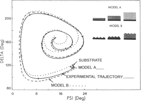
3. As a final example, SE data for the early growth of a PECVD amorphous Si0.65Ge0.35:H film on a chromium substrate are depicted in Fig. 10-8. Of two possible growth modes that can account for the observed Δ–Ψ spiral trajectory, it appears the nucleation of hemispherical caps followed by coalescence rather than layer growth is the operative mechanism.
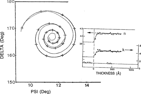
Figure 10-7 Ellipsometry measurement of AlGaAs–GaAs transition in the same organometallic CVD system. (a) Experimental trajectory of Δ and ψ, and comparison with theoretical growth model (solid line) with crosses corresponding to 100-Â increments in thickness. (b) Refractive index (n) and absorption coefficient (k) as a function of GaAs film thickness.
(Reproduced with permission from Annual Reviews Inc. From Ref. 10.)
10.2.5 MECHANICAL TECHNIQUES FOR MEASURING FILM THICKNESS
10.2.5.1 Profilometry
Paralleling the operation of a phonograph needle on a record, profilometry consists of electromagnetically sensing the mechanical movement of a stylus as it traces the topography of a film–substrate step. The step can be made by masking or etching, during or after deposition, respectively. Diamond styli with cone angles of either 45° or 60° and tip radii ranging from 0.2 to 25 μm are commercially available for this purpose. The stylus force typically spans a range from 0.1 to 50 mg, enabling step heights from 50 Å to 800 μm to be measured; vertical magnifications of a few thousand up to ∼ 1 million times are possible. Film thickness is directly read out as the height of the resulting step-contour trace. Vertical height resolutions of ∼ 1 Å are possible, and the reproducibility of successive scans is within ± 10 Å in a 1000-Å thick film. Several factors which limit the accuracy of stylus measurements are:
1. Stylus penetration and scratching of films. This is sometimes a problem in very soft films, e.g., In, Sn.
2. Substrate roughness. Excessive noise is introduced into the measurement as a result and this creates uncertainty in the position of the step.
3. Vibration of the equipment. Proper shock mounting and rigid supports are essential to minimize background vibrations.
In modern instruments the leveling and measurement functions are computer controlled. The vertical stylus movement is digitized and data can be processed to magnify areas of interest and yield best-profile fits. Calibration profiles are available for standardization of measurements.
Both thin films and thick coatings are amenable to profilometry. One of the interesting applications is to determine the flatness and depth of a sputtered crater during depth-profiling analysis by Auger electron spectroscopy (AES)(Section 10.4.4) or secondary ion mass spectrometry (SIMS) (Section 10.4.8). In this technique a circular region on the film surface is sputtered away and an electron (AES) or ion (SIMS) probe beam ideally analyzes the flat bottom of the crater formed. Such a crater profile generated during SIMS analysis is shown in Fig. 10-9 where the total depth sputtered exceeds 2.5 μm. Since the sputtering times are known, this information can be converted into an equivalent depth scale for use in determination of precise concentration profiles. If the crater walls are slanted rather than vertical, the analyzing beam may not sample the bottom flat surface but some portion of the side wall. This leads to errors in the depth profile which must be corrected for.
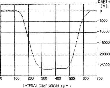
Figure 10-9 Profilometer trace of crater in InP produced during raster scanning of 12.5 keV Cs+ ion beam across surface.
(Courtesy of H. Luftman, AT&T Bell Laboratories.)
Related to probing sputtered craters is the demanding application of profiling trench depths in integrated circuits. Depending on trench width, the maximum depth that can be accessed depends on the stylus radius. For example, with a 0.2 μm tip radius traversing a 1 μm wide trench, a trench depth of 0.66 μm could be reached; with a 2.5 μm tip radius the maximum depth that can be probed is only 0.05 μm (Ref. 15).
10.2.5.2 Quartz Crystal Microbalances
The universally employed technique for in situ monitoring of the thickness of physical vapor-deposited films is based on the use of quartz crystal oscillators. Because the mass of the film is sensed the technique is also known as the quartz crystal microbalance method. Interestingly, very delicate and novel mechanical microbalances have been constructed and widely employed in the past to monitor film thickness during deposition. Microbalance designs have relied on such effects as the elongation of a thin quartz-fiber helix, the torsion of a wire, or the deflection of a pivot-mounted beam. Sensitive optical and, more commonly, electromechanical transducers and compensators for null measurements have been employed, enabling detection of film deposits weighing ∼ 10−8 g. If the film density is known, its thickness can be determined (Ref. 16).
To understand the operation of quartz crystal oscillators, consider homogeneous elastic plates set into mechanical vibration. These have resonant frequencies which depend on their dimensions, elastic moduli, and importantly on density. Additional mass in the form of a deposited thin film alters (lowers) the resonant frequency by effectively changing the properties of the composite vibrating plate. In practice, AT quartz crystals, i.e., cut ∼ 35° with respect to the c axis, are employed. These same piezoelectric crystals are used for precise timing in watches and electronic instruments. They are powered through metal film electrodes on both wide faces of the crystal and are mounted within the deposition chamber close to the substrate. The fundamental frequency, f, of the shear vibrational mode is given by f = νq/2dq where vq is the elastic wave velocity and dq is the plate thickness; dq is also equal to half the wavelength of the transverse wave. If mass δm deposits on one of the crystal electrodes, the film/crystal thickness increases by an amount given by δd = δm/Aρf, where A and ρf are the film area and density, respectively. Combination of these two equations yields a frequency change given by
where C = νq/2 is defined as the frequency constant whose value is 1656 kHz-mm for AT cut quartz. In deriving Eq. 10-12 we have assumed that the addition of a small foreign film mass can be treated as an equivalent mass change of the quartz crystal. The formula is not rigorously correct because the elastic properties of the film are not the same as those of quartz and A is generally not equal to the total crystal face area. These effects greatly complicate the frequency-response analysis. Nevertheless, as long as the accumulated mass deposited on the crystal does not shift the resonant frequency by a few percent of its original value, δf varies linearly with δm.
To appreciate the kind of numbers involved, we note that a 6 MHz crystal is commonly employed. Since a frequency shift of 1 Hz is readily measurable, Eq. 10-12 reveals that this is equivalent to a mass of Al = 1.24 × 10⁻⁸ gms, and if A = 1cm2, to a film thickness of 0.46 Å. This sensitivity is suitable for most applications. It can be enhanced, however, by more than an order of magnitude by employing thinner crystals with higher resonant frequencies, and by detecting smaller frequency shifts.
Since differences rather than absolute magnitudes are usually easier to detect with precision, the frequency shift is usually measured by beating the crystal signal against that from a reference (undeposited) crystal and subtracting. Quartz crystal oscillators are commonly employed for the measurement of deposition rate rather than film thickness. Therefore, commercial rate monitors contain circuitry to mathematically differentiate the frequency change with respect to time, display the rate, and provide feedback to control the power delivered to evaporation sources. In these functions it is essential to eliminate uncertainty in the frequency shift measurement. A potentially important source of error arises from the temperature increase of the crystal due to radiant-heat exposure from the evaporant source, and from the heat of condensation liberated by depositing atoms. Typically, temperature increases of a few degrees Celsius above that of the reference crystal result in frequency shifts of 10–100 Hz which are equivalent to a mass change of 10−7 to 10−6 g/cm2. For this reason crystals are enclosed in water-cooled shrouds having a small entrance aperture to sample the evaporant stream. Lastly, precise work requires a correction due to the geometry of the monitor relative to the substrate.
10.2.5.3 Ultrasonic Multilayer-Film Metrology
Previously we noted that spectral reflectance (Section 10.2.3.4) and spectroscopic ellipsometry (Section 10.2.4.5) techniques enabled the accurate determination of the thickness of individual films within layered dielectric stacks. But this is not possible for opaque metal films because light cannot penetrate through them. In such cases film thickness is usually inferred from sheet resistance measurements knowing the film resistivity. For a stack of metal films consisting of individual blanket layers this means tedious sequential determinations following successive depositions. However, because of exciting recent advances in instrumentation there appears to be a much better option. It is now possible to determine the thickness of each film in a multilayer stack in a single measurement that can be made in a few seconds!
To appreciate the significance of the technique, consider the following metrology requirements for metallizations during the processing of Si wafers (Ref. 17):
1. Capability of simultaneously measuring the thickness of up to six (or more) stacked optically opaque films
2. A noncontact and nondestructive technique
3. Probe spot sizes of 10 to 20 μm diameter which are compatible with the size of test structures
4. Measurement time no longer than the process deposition time
5. Film thickness determinations from ∼ 2 nm to a few micrometers
6. A high degree of precision, accuracy (1–2%), and reproducibility (1%) in measurement
7. Robust operation and a high level of automation so that it can be used in manufacturing environments
Satisfying this wish list of requirements, particularly the first one, was unimaginable a few years ago. However, there are now practical commercial instruments capitalizing on picosecond ultrasonic laser-sonar methods that meet each of these demands (Ref. 18).
In this photoacoustic technique an ultrafast laser produces a short (˜ 10−13 s) light pulse that impinges on the film surface. Absorption of this light causes a localized rapid thermal expansion that in turn launches an acoustic wave which propagates away from the surface with the speed of sound (νs). The local temperature rise of a few degrees Celsius and subsequent heat dissipation over a few nanoseconds, based on a pulse energy of ∼0.5 nJ, play no further role in the measurement. As the sound wave encounters subsurface film interfaces part of the wave reflects back while the remainder propagates further. When the echo from the first interface reaches the surface it changes its reflectivity by perhaps only one part in 105.A second light pulse, diverted from the initial laser pump light by a beam splitter, detects this change but the signal is delayed by the time (t) it takes sound to twice traverse the film thickness (d), i.e.,
The measurement, with characteristics of both sonar and interferometry, is capable of measuring distance traveled to within an angstrom.
In Fig. 10-10a we see that a time of 42 ps elapses between a sequence of echoes obtained from a TiN film deposited on a Si substrate. If it is independently known that νs = 9.5 nm/ps (9500 m/s), simple calculation yields a film thickness of 200 nm. Now consider a 20 nm Ti film sandwiched between the TiN and Si. A more complicated reflectivity response is recorded in Fig. 10-10b because sound now reflects first from the TiN/Ti interface and then from the Ti/Si interface. The 6.5-ps interval between the first and second peaks corresponds to the time it takes sound to travel through the buried Ti film and echo back from the Si surface. From this information we deduce that vs is equal to 2 × 20 nm/6.5 ps or 6150 m/s in Ti.
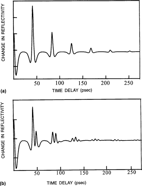
Figure 10-10 Time-dependent change in reflectivity for (a) 200 nm TiN/Si and (b) 200 nm TiN/20 nm Ti/Si.
(Courtesy of G. J. Collins, Rudolph Technologies Inc. From Ref. 17.)
In addition to film thickness measurement, picosecond ultrasonics have the important capability of characterizing more subtle material and structural properties such as film density and interfacial roughness and adhesion. Such information is provided by the relative amplitudes of successive echoes and the shape and widths of the reflected signals. For example, the echo amplitude decay rate depends on the acoustic reflection coefficient (Ra), a quantity that is film-density dependent. In addition, Ra is also a sensitive measure of the strength of interfacial bonding. A film that is poorly bonded to another film or the substrate inefficiently transfers acoustic energy across the interface. Therefore, more energy is reflected and Ra would be larger than the value obtained for a clean interface. Images of Ra as a function of position across wafer surfaces can thus assess the quality of blanket films on wafers. Analogous ultrasonic imaging methods have been very successfully employed in exposing delamination of chips from substrates in plastic encapsulated packages (Ref. 19). Other applications to multilayer films have been reviewed by Stoner et al. (Ref. 20).
10.3 STRUCTURAL CHARACTERIZATION OF FILMS AND SURFACES
10.3.1 INTRODUCTION
There are several hierarchies of structural information which are of interest to thin-film scientists and technologists in research, process development, and reliability and failure analysis activities. These are listed next in roughly ascending order of structural resolution required.
1. The first broadly deals with metrology of patterned films where issues of lateral or depth dimensions and tolerances, uniformity of thickness and coverage, completeness of etching, etc., are of concern.
2. Secondly, film surface topography and microstructure in plan view including grain size and shape, existence of compounds, presence of hillocks or whiskers, evidence of film voids, microcracking or lack of adhesion, etc., are of interest.
3. Next are cross-sectional views of multilayer structures exposing interfacial regions, columnar grain morphology, and substrate interactions. Such images are crucial in microelectronics and optical coating technologies, enabling direct verification of device dimensions and structural defects in devices.
4. Somewhat more challenging are the high-resolution lattice images of both plan-view and transverse film sections. Among the applications here are defect structures in films and devices, structure of grain boundaries, identification of phases, and a host of issues related to epitaxial structures, e.g., the crystallographic orientations, direct imaging of atoms at interfaces, interfacial quality and defects, and perfection of assorted thin film superlattices.
5. Finally, there is structural information required of substrate and film surfaces such as the details of film-nucleation and growth processes, crystallography of deposits, and reconstruction of surface layers.
In addressing all these needs there is a growing arsenal of techniques that includes optical, electron, and scanning probe microscopes. Thus the scanning electron microscope (SEM), and occasionally, the reflection metallurgical microscope would primarily be used to obtain the required information included under items 1, 2, and 3. The transmission electron microscope (TEM) addresses item 3 as well. Augmented perhaps by X-ray diffraction methods, the TEM is indispensable for item 4. And finally to confront item 5 there is the atomic force microscope (AFM) and the scanning tunneling microscope (STM). This section discusses those techniques that have the common objective of structurally characterizing films and surfaces. Together with a description of their operation and an introduction to the interpretation of results they provide, the advantages and disadvantages of each will be noted.
10.3.2 SCANNING ELECTRON MICROSCOPY
Because seeing is believing and understanding, the SEM is perhaps the most widely employed thin-film and coating characterization instrument (Refs. 21, 22). There is an interesting distinction between the SEM and TEM. The latter is a true microscope in that all image information is acquired simultaneously or in parallel. In the SEM, however, only a small portion of the total image is probed at any instant and the image builds up serially by scanning the probe. Strictly speaking, the SEM has more in common with the scanning Auger electron (Section 10.4.4) and SIMS (Section 4.4.8) microprobes than a traditional microscope.
A schematic of the typical SEM is shown in Fig. 10-11. Electrons thermionically emitted from a tungsten or LaB6-cathode filament are drawn to an anode and focused by two successive condenser lenses into a beam with a very fine spot size that is typically 10 Å in diameter. Pairs of scanning coils located at the objective lens deflect the beam either linearly or in raster fashion over a rectangular area of the specimen surface. Electron beams having energies ranging from a few keV to 50 keV, with 30 keV a common value, are utilized. Upon impinging on the specimen, the primary electrons decelerate and in losing energy, transfer it inelastically to other atomic electrons and to the lattice. Through continuous random scattering events the primary beam effectively spreads and fills a teardrop-shaped interaction volume (Fig. 10-12a) with a multitude of electronic excitations. The result is a distribution of electrons which manage to leave the specimen with an energy spectrum shown schematically in Fig. 10-12b. In addition, target X-rays are emitted and other signals such as light, heat, and specimen current are produced; the sources of their origin can be imaged with appropriate detectors. Various SEM techniques are differentiated on the basis of what is subsequently detected and imaged. Several of these are indicated next.
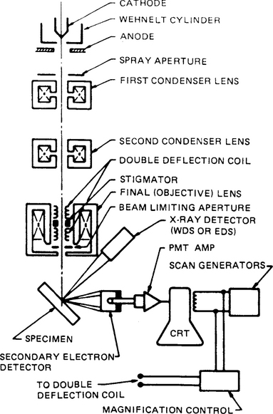
Figure 10-11 Schematic of the scanning electron microscope.
(From Ref. 21 with permission from Plenum Publishing Corp.)

Figure 10-12 (a) Electron and photon signals emanating from tear-shaped interaction volume during electron-beam impingement on specimen surface. (b) Energy spectrum of electrons emitted from specimen surface. (c) Effect of surface topography on electron emission.
10.3.2.1 Secondary Electrons
The most common imaging mode relies on detection of this very lowest portion of the emitted energy distribution. Their very low energy means they originate from a subsurface depth of no larger than several angstroms. The signal is captured by a detector consisting of a scintillator/photomultiplier combination and the output serves to modulate the intensity of a cathode-ray tube (CRT) which is rastered in synchronism with the raster-scanned primary beam. Image magnification is then simply given by the ratio of scan length on the CRT to that on the specimen. Resolution specifications quoted on research-quality SEMs are less than 2 nm. Great depth of focus enables images of beautiful three-dimensional quality to be obtained from nonplanar surfaces. The contrast variation obtained can be understood with reference to Fig. 10-12c. Sloping surfaces produce a greater secondary-electron yield because the portion of the interaction volume projected on the emission region is larger than on a horizontal surface. Similarly, edges will appear even brighter. Several examples of secondary-electron SEM images have been reproduced in various places throughout the book.
10.3.2.2 Backscattered Electrons
These are the high-energy electrons which are elastically scattered and essentially possess the same energy as the incident electrons. The probability of backscattering increases with the atomic number Z of the sample material. Since the backscattered fraction is not a very strong function of Z (varying very roughly as ∼ 0.05Z1/2) elemental identification is not feasible from such information. Nevertheless, useful contrast can develop between specimen regions that differ widely in Z. Since the escape depth for high-energy backscattered electrons is much greater than for low-energy secondaries, there is much less topological contrast in the images,
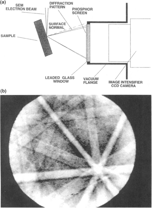
An interesting phenomenon which makes use of backscattered electrons is electron backscatter diffraction (EBSD), also known as backscatter Kikuchi diffraction (BKD). Since an important application to the microtexture of polycrystalline films was previously described in Section 9.4.5, it is worth briefly noting the principle of the technique here. As the finely focused electron beam of an SEM (Fig. 10-13a) penetrates a crystalline specimen, i.e., a grain, electrons are inelastically scattered and lose angular correlation with the primary beam. In the process, a point source of electrons effectively forms and it Bragg diffracts from the sample lattice. Electrons, scattered at large angles in the shape of conelike beams, intercept a flat detector and produce an image consisting of intersecting hyperbolic sections as shown in Fig. 10-13b. Computer analysis of these geometrically complex EBSD patterns enables the crystallographic orientation of individual grains to be extracted. As a result, a microtexture pole figure can build up point by point as the beam scans from grain to grain.
10.3.2.3 X-Rays
An SEM is like a large X-ray vacuum tube used in conventional X-ray diffraction systems. Electrons emitted from the filament (cathode) are accelerated to high energies where they strike the specimen target (anode).
In the process, X-rays characteristic of atoms in the irradiated area are emitted. By analyzing their energies the atoms can be identified and by counting the numbers of X-rays emitted, the concentration of atoms in the specimen can be determined. Instrumentation for this major X-ray spectroscopy technique, known as X-ray energy dispersive analysis (EDX), is practically always attached to the SEM column. X-ray spectroscopy will be further discussed in Section 10.4.3.
10.3.3 TRANSMISSION ELECTRON MICROSCOPY
10.3.3.1 Introduction
Normally a research tool, the transmission electron microscope (TEM) is indispensable for the structural imaging of nanometer-sized features. In comparison, the resolution of the SEM is about an order of magnitude poorer. As its name implies, the TEM is used to obtain structural information from specimens thin enough to transmit electrons. Thin films are, therefore, ideal for study but they must be removed from electron-impenetrable substrates prior to insertion in the TEM.
As a gross simplification, the TEM may be compared to a slide projector with the slide (specimen) illuminated by light (electron beam) that first passes through the condenser lens (electromagnetic condenser lens). The transmitted light forms an image that is magnified by the projector lens (electromagnetic objective and projector lenses) and viewed on a screen (or photographed). In operation, electrons are thermionically emitted from the gun and typically accelerated to anywhere from 125 to 300 keV, or higher (e.g., 1 MeV) in some microscopes. High magnification in TEM methods is a result of the small effective wavelengths (λ) employed. According to the deBroglie relationship,
where m and q are the electron mass and charge, and ν is the potential difference. Electrons of 100 keV energy have wavelengths of 0.037 Å and are capable of effectively transmitting through about 0.6 μm of Si. In operation, electrons are projected onto the specimen by the condenser lens system. The scattering processes they undergo during their passage through the specimen determine the kind of information obtained. Elastic scattering, involving no energy loss when electrons interact with the potential field of the ion cores, gives rise to diffraction patterns. Inelastic interactions between beam and matrix electrons at heterogeneities such as grain boundaries, dislocations, second-phase particles, defects, and density variations cause complex absorption and scattering effects leading to a spatial variation in the intensity of the transmitted beam. Primary and diffracted electron beams that emerge from the specimen are now made to pass through a series of postspecimen lenses. The objective lens produces the first image of the object and is, therefore, required to be the most perfect of the lenses. Just how the beams reaching the back focal plane of the objective lens are subsequently processed distinguishes the different methods of operation.
10.3.3.2 operational Modes
There are two very broad modes of TEM operation, namely imaging and analytical. In the former, structural images ranging from low magnification to atomic resolution are directly revealed, whereas in the latter structural information is indirectly revealed through analysis of diffracted beam geometries and energies. These modes are differentiated in Figs. 10-14a and 10-14b, where the lenses, beam path, and method of image formation are schematically indicated. Each of the techniques depicted is briefly described in turn below.
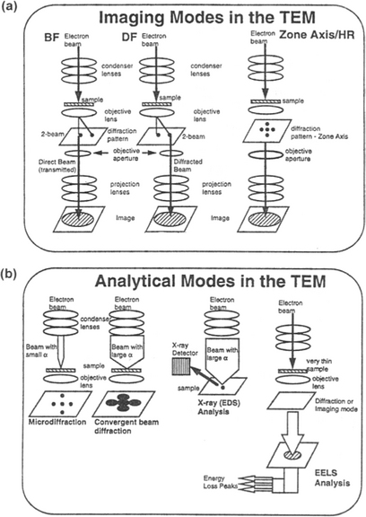
Figure 10-14 Two broad modes of TEM operation. (a) Imaging modes. (b) Analytical modes.
(From V. S. Kaushik, IEEE International Reliability Physics Symposium, Tutorial Notes, p. 3.64, 1994. Reprinted with permission of the author.)
1. Bright-field imaging (BF). Also known as conventional TEM, bright-field imaging intentionally excludes all diffracted beams and only allows the central beam through. This is done by placing suitably sized apertures in the back focal plane of the objective lens. Intermediate and projection lenses then magnify this central beam to provide images of the microstructure and morphology of features.
2. Dark-field imaging (DF). Dark-field images are also formed by magnifying a single beam; this time one of the diffracted beams is chosen by means of an aperture which blocks both the central beam and the other diffracted beams. The micrograph of alternating 40 Å wide films in the GaAs–Al0.5Ga0.5As superlattice structure shown in Fig. 10-15 is a dark-field image employing the 200 diffracted beam. In both bright- and dark-field imaging we speak of amplitude contrast because diffracted beams with their phase relationships are excluded from the imaging sequence.
3. Lattice imaging. In this now-popular method of imaging periodic structures with atomic resolution, the primary transmitted and one or more of the diffracted beams are made to recombine, thus preserving both beam amplitudes and phases. High-resolution lattice images of the interfacial region between epitaxial CoSi2 and Si (Fig. 1-4) and the polysilicon/oxide/silicon structure (Fig. 11-10) are examples of this remarkable technique.
4. Diffraction. Diffraction yields crystallographic and orientation effect information on structural features, defects, and phases. Microdiffraction in localized regions is conveyed in patterns that look much like the spotted arrays in Fig. 8-33 or Fig. 9-24 when crystalline material is analyzed. For polycrystalline and amorphous materials the spots give way to diffraction rings of varying sharpness and width. Convergent-beam electron diffraction enables detection of less than ![]() ±0.001 Å variations in lattice parameter with high precision. This sensitivity makes it possible, for example, to measure deviations in texture orientations and strains in individual grains of polycrystalline films.
±0.001 Å variations in lattice parameter with high precision. This sensitivity makes it possible, for example, to measure deviations in texture orientations and strains in individual grains of polycrystalline films.
5. X-ray spectroscopy. This analytical capability, otherwise known as X-ray energy dispersive analysis (EDX), allows elemental identification through measurement of characteristic X-ray energies. Core electron transitions which are discussed in Section 10.4.2 are the basis of the technique.
6. Electron energy loss spectroscopy (EELS). Through energy analysis of the transmitted electron beam, composition analysis is possible. EELS is particularly useful for detecting low-Z elements.
Figure 10-15 Dark-field TEM image of alternating 40 Å wide GaAs–Ga0.5Al0.5As superlattice films. Light bands contain Al.
(Courtesy of S. Nakahara, AT&T Bell Laboratories.)
The theory and practice of electron optics and various TEM techniques are beyond our scope but have been detailed in several excellent books on the subject (Refs. 23, 24).
10.3.3.3 TEM Cross-Sections
Perhaps the most dramatic images of film structures and devices are those taken in cross section. In this important technique, specimens that are already thin in one dimension are now thinned in the transverse direction; it is like imaging this page in edge view rather than in the plane the words appear on. What is involved in the case of integrated circuits is cleaving a number of wafer specimens transversely, bonding these slivers in an epoxy button, and thinning them by grinding and polishing. Finally, the resulting disk is ion milled until a hole appears. By preparing many specimens simultaneously the probability of capturing images from desired device features is enhanced.
As an outstanding example of a TEM cross-sectional image, consider the nanotransistor shown in Fig. 10-16. This field-effect transistor structure has a 61 nm channel (182 atoms long) and a gate oxide, barely visible beneath poly-Si, that is only 1.2 nm or about three atoms thick (see Fig. 11-10). Smaller features together with shallower source- and drain-junction depths, high-aspect-ratio polysilicon, and gate electrodes can be expected in the future. Lower operating voltages and higher transconductances of nanotransistors mean impressive power savings of 60–160 times relative to present-day devices.

10.3.3.4 Focused Ion Beam Microscopy
The use of focused ion beams (FIB) represents a recent major advance in TEM sample preparation as well as for microscopy in its own right. Briefly, the FIB resembles an SEM but instead of electrons, gallium ions generated in a liquid-metal ion source are employed as the imaging vehicle. In the ion-optical column these ions are electrostatically focused into a fine beam that raster scans the specimen surface releasing secondary electrons for structural imaging. When operated as a high-resolution microscope the FIB has some advantages as well as disadvantages relative to the SEM and TEM. The FIB image of an Al–0.5% Cu film shown in Fig. 10-17a reveals grain orientation contrast unlike secondary electron SEM imaging; also unlike TEM methods, thick specimens that require no sample preparation can be imaged by FIB microscopy. In Fig. 10-17b the SEM electron backscatter (EBSD) image (see Sections 9.4.5 and 10.3.2.2) demonstrates how well the techniques correlate with each other.

Figure 10-17 (Left) FIB secondary electron image of Al–0.5% Cu blanket film taken with a 30 keV Ga beam. Note: A grain tracing is overlayed. (Right) EBSD pattern map of same area.
(Courtesy of L. Gignac, IBM, T. J. Watson Research Center.)
At the same time the Ga ions help form images, they contaminate specimens, introduce artifacts, and sputter away the material being observed. The latter undesirable feature for imaging is capitalized upon in preparing TEM cross sections, where it has eased the drudgery and eliminated the element of chance in locating features for examination (Ref. 25). Operating like a milling machine, the 10 to 25 keV Ga beam precisely etches material from submicron regions of specimens. Suitably thinned features can then be subsequently examined in the TEM. This sample preparation technique illustrated in Fig. 10-18 has greatly advanced structural characterization methodology in scientific and technological, e.g., failure analysis, applications.
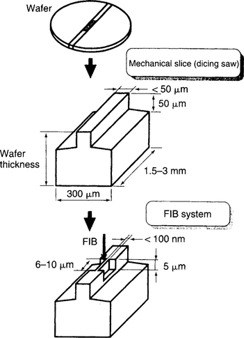
Figure 10-18 Cross-section sample preparation for TEM employing rough mechanical slicing followed by FIB milling techniques to remove submicron layers of material.
(From Ref. 25. Reprinted by permission.)
10.3.4 X-RAY DIFFRACTION
This very important experimental technique has long been used to address all issues related to the crystal structure of bulk solids including lattice constants and crystallography, identification of unknown materials, orientation of single crystals and preferred orientation of polycrystals, defects, stresses, etc. Extension of X-ray diffraction methods to thin films has not been pursued with vigor for two main reasons: First, the great penetrating power of X-rays means that with typical incident angles, their path length through films is too short to produce diffracted beams of sufficient intensity. Under such conditions the substrate, rather than the film, dominates the scattered X-ray signal; thus, diffraction peaks from films require long counting times. Second, the TEM provides similar diffraction information with the added capability of performing analysis over very small selected areas. Nevertheless X-ray methods have advantages because they are nondestructive and do not require elaborate sample preparation or film removal from the substrate. Two applications to thin films follow.
10.3.4.1 Monitoring Interdiffusion in Thin Films
Consider a specimen consisting of consecutively evaporated polycrystalline films of Ag, Au, Ag, and Pb on fused quartz (Fig. 10-19b). After the composite structure is annealed at 200°C for 24 h it is desired to know the composition of the reaction products. To accomplish this by X-ray methods the films must appear to be thicker to the beam than they actually are. Employing a grazing angle of incidence y = 5° makes the films effectively 12 times thicker. The Seeman– Bohlin diffraction geometry (Fig. 10-19a) is used with the focal point of the X-ray source, film specimen, and detector slit all located on the circumference of one great circle. Each of the diffracted peaks (Fig. 10-19c) appear at different angles which are sequentially swept through as the X-ray detector moves along the circumference. All the while, a servomotor rotates the detector to keep it aimed at the specimen and preserve the overall focusing geometry.
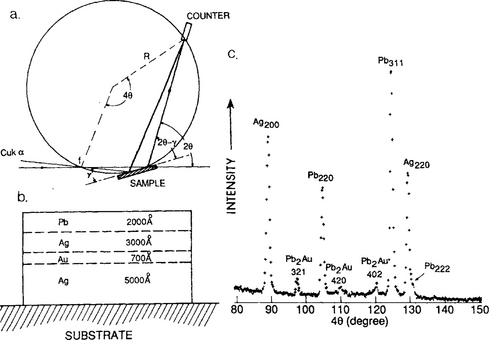
Figure 10-19 (a) Seeman–Bohlin diffraction geometry. f = effective location of X-ray source, y = angle of incidence, θ = Bragg angle. (b) Schematic of layered film specimen. (c) A selected portion of the diffraction pattern with reflections from Ag, Pb, and Pb2Au shown.
(From K. N. Tu, J. Appl. Phys. 43, 1303 (1972). (Courtesy of K. N. Tu, IBM, T. J. Watson Research Center.)
The fact that Pb2Au peaks emerged indicates that Au atoms diffused through the polycrystalline Ag layer and then reacted with the Pb. Grain boundaries in Ag were the likely diffusion path because no penetration of single-crystal Ag films by Au was observed.
10.3.4.2 Analysis of Epitaxial Films
Let us suppose we wish to nondestructively measure the composition of a ternary epitaxial film of A1xGa1–xAs on GaAs to an accuracy of 2%. One way to do this is to make use of the connection between the lattice parameter a0 and x. Vegard’s law then suggests that a0 must be measured to a precision of
or 1 part in more than 35,000. This is quite a formidable challenge and neither LEED nor RHEED can even remotely approach such a capability. X-ray diffraction methods can, however, but not easily. By virtue of Bragg’s law (Eq. 1-2), differentiation yields
This equation reveals the inadequacy of conventional X-ray diffraction methods in meeting the required measurement precision. For example, typical CuKα (λ = 1.5406 Å) radiation from an X-ray tube exhibits a so-called spectral dispersion of 0.00046 Å, so that Δλ/λ = 0.0003. This causes unacceptable diffraction peak broadening. In addition, the angular divergence of the beam must be several seconds of arc and it is not possible to achieve this with usual slit-type collimation.
For the foregoing reasons the high-resolution double-crystal diffractometer, shown schematically in Fig. 10-20, is indispensable. It has three special features:
1. Very high angular stepping accuracy on the θ axis (i.e., ![]() 1 arc second)
1 arc second)
2. Excellent angular collimation of the incident X-ray beam (i.e., < 10 arc seconds)
3. Elimination of peak broadening due to spectral dispersion
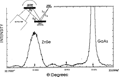
Figure 10-20 Rocking curve for (004) reflection of ZnSe on GaAs.
(Courtesy of B. Greenberg Philips Laboratories, North American Philips Corp.) (Inset) Schematic of high-resolution double-crystal diffractometer. (From A. T. Macrander, Ann. Rev. Mater. Sci. 18, 283, 1988.)
The diffractometer consists of a point-focus X-ray source of monochromatic radiation which falls on a first collimator crystal composed of the same material as the sample epitaxial film (second crystal). When the Bragg condition is satisfied both crystals are precisely parallel. The Bragg condition is simultaneously satisfied for all source wavelength components, i.e., no wavelength dispersion. During measurement, the sample is rotated or rocked through a very small angular range. The resulting rocking curve diffraction pattern contains the very intense substrate peak which serves as the internal standard against which the position of the low-intensity epitaxial film peak is measured.
In the following example the power and importance of the technique is illustrated. A rocking curve of an 1100 Å ZnSe film grown epitaxially on a (001) GaAs substrate is shown in Fig. 10-20 for the (004) reflection. In GaAs a0 = 5.6537 Å and a(004) = 1.4134 Å. Since λ = 1.5406 Å, Bragg’s law yields θ = 33.025°. For ZnSe with a0 = 5.6690 Å, a(004) = 1.4173 Å and the expected Bragg angle for unstrained ZnSe is 32.923°. But the actual (004) peak appears at 32.802° which corresponds to a(004) = 1.4219 Å. To interpret these findings it should be noted that the misfit (Eq. 8-1) in this system is – 0.27% and hence ZnSe is biaxially compressed in the film plane. But since the film thickness is less than dc (Eq. 8-5), it has grown pseudomorphically with GaAs; we can therefore assume that ZnSe has the same lattice constant as GaAs in the interfacial plane. However, normal to this plane the ZnSe lattice expands and assumes a tetragonal distortion. The measured increase in the (004) interplanar spacing of ZnSe is thus consistent with this explanation.
10.3.5 SCANNING PROBE MICROSCOPIES
10.3.5.1 Introduction
When Binnig and Rohrer invented the scanning tunneling microscope (STM) in 1981 they could scarcely have imagined that its impact would eventually encompass disciplines as diverse as surface science, thin-film technology, and cellular biology. The STM and variants of it, most notably the atomic force microscope (AFM), are collectively known as scanning-probe microscopes (SPMs). These instruments are imaging tools that have a resolution range spanning the capabilities of the SEM at one extreme and TEM lattice imaging at the other. In addition, assorted physical properties such as surface conductivity, elastic moduli, static-charge distributions, and magnetic fields have been measured by SPM methods, suggesting a sense of the breadth of applications. Aspects of scanning-probe microscopies are reviewed in Refs. 26-28.
10.3.5.2 Scanning Tunneling Microscopy
The STM, the progenitor of all subsequent scanning-probe microscopes, won the 1986 Nobel prize in physics for its inventors. It was not the first microscope that could image atoms, however. Some three decades earlier E. Müller invented the field ion microscope (FIM). Though not as popular a surface-science tool as it once was, the FIM has been employed over the years in studies of defects, surface diffusion, crystallography, desorption, and alloying (Ref. 29). In this microscope (Fig. 10-21a) the surface of a strong metal tip, sharpened to a radius of curvature less than ∼ 0.1 μm, is the specimen being imaged. The cryogenically cooled tip is contained within a system pumped to high vacuum (˜ 10−10 torr) and then backfilled with an imaging gas, typically helium. When the tip is raised to a high positive potential (˜ 10 kV), very high electric fields (several hundred MV/cm) are generated in the vicinity of tip atom projections. This has the effect of stripping electrons from the gas atoms into the tip atoms through tunneling from the former to the latter. The resulting positive He ions then fly off the metal along the electric-field lines and light up the grounded fluorescent screen, providing a projected image of the atomic arrangement on the terraced terrain of the tip, shown in Fig. 10-21b for tungsten. Terms that are italicized may be viewed as disadvantages of FIM because they correspond to limitations in specimens that can be imaged, experimental difficulties, and complexities in interpreting images.


Figure 10-21 (a) Schematic of a field-ion microscope employing helium ions. (b) Field-ion microscope image of tungsten tip.
(From E. W. Müller, Advances in Electronics and Electron Physics, Vol. 13. Reprinted with the permission of Academic Press, Inc.)
The STM eliminates many, but not all of these restrictions and shortcomings, i.e., all conductors are imageable in principle and there is less danger of distorting and altering surface features in high electric fields. Importantly, unlike other indirect techniques for determining surface crystallography that depend on the amplitude and phases of scattered electron, photon or ion waves, the STM enables direct imaging of atoms. Like the FIM, the STM also employs a metal needle or probe tip and it is etched to almost an atomic radius. But this tip serves as a conductive electrode probe and is not the specimen being observed. In operation the tip is normally brought to within about 1 nm of the specimen surface. There it is rastered in atomic-scale increments along both x and y surface directions by means of piezoelectric transducers, as shown in Fig. 10-22. An electron tunneling current, i, flows across the narrow vacuum-gap distance s between tip and specimen when a voltage VT (typically millivolts to a few volts) is applied between them. This current arises when electrons occupying filled electron states in a negatively biased tip tunnel into unfilled states in the specimen; electrons flow in the reverse direction when the tip–specimen polarity is reversed. Theory supported by measurement indicates that for small values of νT the current is given by
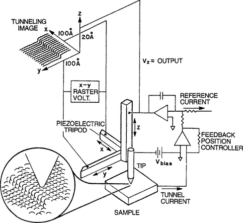
Figure 10-22 Schematic illustration of the scanning tunneling microscope. The tunneling current is maintained constant during surface scanning through electronic feedback.
(From J. A. Golovchenko, Science 232, 48, 1986. Copyright © 1986 by the American Association for the Advancement of Science. Reprinted with the permission of Science and J. A. Golovchenko, Harvard University.)
where a and A are constants and ϕ is the average work function. The interdependence of i, VT, and s for a given ϕ tightly fixes experimental conditions such that the tunneling current is typically a very steep function of s.
There are two basic modes of operating an STM. In the first, the tunnel current is maintained constant during lateral scanning by keeping s constant as the tip rides up and down over the atomic terrain. This is accomplished through feedback electronics which continually adjusts the tip height. Alternatively, the tip scans at a preset height so that the tunnel current varies periodically in concert with the atomic-scale surface corrugations. In either case the electronic signal variations are converted into an image such as the one shown for a reconstructed (111) Si surface (Fig. 7-9).
10.3.5.3 An Atomic Corral
One of the most intriguing features of the STM is its ability to move individual adsorbed atoms to selective sites on a surface. Since the tip exerts both van der Waals and electrostatic forces on such atoms they can be extracted, dragged, and displaced along the surface by simply varying the tip position and bias voltage (Ref. 30). An early example of this was the well-publicized manipulation of 35 individual xenon atoms on a nickel surface to spell out the IBM logo. Even more fascinating from a scientific point of view is the 14.3-nm diameter quantum corral shown in Fig. 10-23 that was created by carefully positioning 48 iron atoms on a (111) copper surface (Ref. 31). Electrons near the surface essentially form a two-dimensional electron gas that is sandwiched between the Cu work function on the vacuum side and a bandgap in the energy levels of the bulk electrons. Free to roam within the corral, the electrons scatter off the confining Fe atom fence. As a result they establish electron-density standing waves corresponding to allowed quantum states in a two-dimensional circular box. This quantum roundup of electrons in the corral should be contrasted with trapping of electrons in quantum wells that arise in layered semiconductor films (Ref. 32). Both experimental arrangements have corroborated very basic predictions of wave mechanics that were previously relegated to texts on theoretical physics.

Figure 10-23 Quantum corral of iron atoms positioned on a (111) copper surface and then imaged by an STM at 4K.
(From cover of Physics Today 46, Nov. (1993); also Ref. 31. Copyright © 1993 by the American Institute for Physics. Reprinted by permission.)
10.3.5.4 Atomic Force Microscopy
Shortly after the STM appeared, the atomic force microscope (AFM) was conceived as a response to the question: if surfaces could be imaged by a current, why not by a force? A major advantage of detecting forces rather than current is that all kinds of material surfaces including metals, semiconductors, and insulators are imageable. The inventors of the AFM realized that in order to mechanically sense atomic-scale surface topography, the sharp tip should be mounted at the end of a soft cantilever spring (Ref. 33). Furthermore, the cantilever spring constant k must be smaller than the spring constant Ks (a) that effectively exists between atoms, and the applied force should not be large enough to displace surface atoms. Treating a vibrating atom as a mass on a spring, the simple theory of the harmonic oscillator indicates that 2πν = (Ks(a)/m)1/2, where ν is the frequency and m is the atomic mass. Since 2πν is typically 1013 Hz and m ![]() 10−25 kg, Ks (a)
10−25 kg, Ks (a) ![]() 10 N/m. In contrast, we know from solid mechanics that the spring constant or force per unit deflection of a cantilever of length l, width w, and depth d is given by k = Ywd3/4l3. Since Young’s modulus (Y) for inorganic materials ranges from ∼ 50 to 1000 × 109 N/m2, large values of l coupled with small values of both w and d are required to reduce the magnitude of k. For example, if the cantilever were made of household aluminum foil with Y = 72 × 109 N/m2, d = 25 × 10−6 m, l = 4 × 10⁻³ m, and w = 1 ×10⁻³ m, k = 4.4 N/m. Presently, AFM cantilevers are micromachined from silicon, silicon dioxide, or silicon nitride and have spring constants ranging from 0.1 to ∼ 50 N/m. Many of the essential experimental features of AFM parallel those of STM. There is a mechanical raster-scanning system (usually piezoelectric), a method to sense the cantilever deflection (usually optical, e.g., interferometry), a feedback system to monitor and control the cantilever force, and a display to convert the force–position data into an image.
10 N/m. In contrast, we know from solid mechanics that the spring constant or force per unit deflection of a cantilever of length l, width w, and depth d is given by k = Ywd3/4l3. Since Young’s modulus (Y) for inorganic materials ranges from ∼ 50 to 1000 × 109 N/m2, large values of l coupled with small values of both w and d are required to reduce the magnitude of k. For example, if the cantilever were made of household aluminum foil with Y = 72 × 109 N/m2, d = 25 × 10−6 m, l = 4 × 10⁻³ m, and w = 1 ×10⁻³ m, k = 4.4 N/m. Presently, AFM cantilevers are micromachined from silicon, silicon dioxide, or silicon nitride and have spring constants ranging from 0.1 to ∼ 50 N/m. Many of the essential experimental features of AFM parallel those of STM. There is a mechanical raster-scanning system (usually piezoelectric), a method to sense the cantilever deflection (usually optical, e.g., interferometry), a feedback system to monitor and control the cantilever force, and a display to convert the force–position data into an image.
There are two basic modes of operation, and they can be understood in terms of Fig. 1-8b if we imagine this well-known curve represents the tip force as a function of tip–specimen separation. When the tip and specimen are widely separated, van der Waals forces cause them to weakly attract. But when they draw too closely together, their electron clouds overlap and electrostatic repulsive forces physically push them apart. In the former noncontact AFM (NC-AFM) mode the cantilever is located tens to hundreds of angstroms from the specimen surface. To prevent surface contact a stiff cantilever is used resulting in low tip–specimen forces of ∼ 10−12 N. Because it is difficult to detect small forces the cantilever is vibrated, typically at 100 to 400 kHz. Changes in vibrational amplitude (due to topography) or resonant frequency (due to force gradients and variations in Ks (a)) are then detected by sensitive AC methods, converted to tip– sample spacings, and ultimately recorded as surface images. Among the advantages of NC-AFM are the ability to probe soft or elastic materials and minimization of both surface contamination and tip degradation. Normally, the spatial resolution of AFMs is poorer than that of STMs. But with sharp probe tips, a stiff cantilever, and operation in ultrahigh vacuum, atomic-resolution surface reconstructions of Si (100) 7 × 7 and Si (100) 2 × 1 have been readily imaged by NCAFM means (Ref. 34).
In the latter or contact AFM mode, also known as the repulsive mode, the tip actually makes physical contact with the surface, and forces in the range of 10−6 to 10−8 N are typically generated.
10.3.5.5 Scanning Probe Applications
Spurred by the promise of nanometer-scale or even atomic resolution with relatively inexpensive instruments capable of imaging all classes of materials under different environmental ambients, there has been an unceasing flood of studies in the past decade having applications to physics, chemistry, and biology. To limit the ensuing discussion it must be appreciated that scanning-probe methods reveal surface properties that may or may not reflect the bulk of the underlying thin film. The list of representative applications to thin films and substrate materials in the scientific and technical areas noted in Table 10-3 is perhaps the most appropriate way to briefly summarize this body of information. For the MFM, CFM, and SThM techniques mentioned in the table special sensing tips are required. For example, most MFM force sensors are composed of etched ferromagnetic materials, e.g., Fe, Ni, while CFM and SThM rely on chemically modified tips and very tiny thermocouples, respectively.
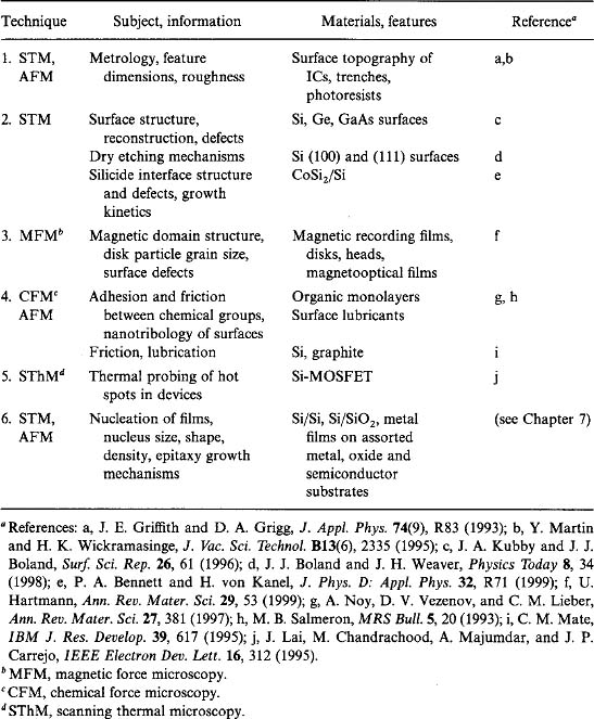
10.4 CHEMICAL CHARACTERIZATION OF SURFACES AND FILMS
10.4.1 INTRODUCTION
In this section we turn our attention to the subject of chemical characterization of thin films. This includes identification of surface and near-surface atoms and compounds, as well as their lateral and depth spatial distributions. To meet these needs an important subset of the analytical techniques listed in Table 10-1 is employed. Space limitations will restrict the discussion to include only the most popular methods (SEM/EDX, AES, XPS, RBS, and SIMS) and variants based on them. The justification for selecting these and not others is that they, together with the SEM and TEM, form the core of the diagnostic facilities associated with all phases of the research, development, processing, and reliability and failure analysis of thin-film electronic and optoelectronic devices. In integrated-circuit technology some of these methods have gained wide acceptance as support tools for manufacturing lines. In addition, all of the associated equipment is now commercially available, albeit at high cost. All excellent film-characterization laboratories are outfitted with the total complement of this equipment. Table 10-4 will help the reader to distinguish among the various chemical analytical methods. Capabilities and limitations of each are indicated and the comparative strengths and weaknesses for particular analytical applications can, therefore, be assessed. The following remarks summarize several of these distinctions.

1. AES, XPS, and SIMS are true surface analytical techniques since the detected electrons and ions are emitted from surface layers less than ∼ 15 Å deep. Provision is made to probe deeper, or depth profile, by sputter etching the film and analyzing the newly exposed surfaces.
2. EDX and RBS generally sample the total thickness of the thin film (˜ 1 μm) and frequently some portion of the substrate as well. Unlike RBS with a depth resolution of ∼ 200 Å, EDX has little depth resolution capability.
3. AES, XPS, and SIMS are broadly capable of detecting, with few exceptions, all of the elements in the periodic table.
4. EDX ordinarily detects elements with Z > 11 and RBS is restricted only to selected combinations of elements whose spectra do not overlap.
5. The detection limits for AES, XPS, EDX, and RBS are similar, ranging from about ∼ 0.1 to 1 at.%. On the other hand, the sensitivity of SIMS is much higher and parts per million can be detected. Even lower concentration levels (˜ 10−6 at.%) are detectable in certain instances.
6. Quantitative chemical analysis with AES and XPS is problematical with error bounds of a few atomic percent. EDX is better and SIMS significantly worse in this regard. Composition standards are essential for quantitative SIMS analysis.
7. Only RBS is quantitatively precise to within an atomic percent or so from first principles and without the use of composition standards. It is the only nondestructive technique which provides simultaneous depth and composition information.
8. The lateral spatial resolution of the region over which analyses can be performed is highest for AES (˜ 500 Å) and poorest for RBS (˜ 1 mm).In between are EDX (˜ 1 μm), SIMS (several μm) and XPS (˜ 0.1 mm). AES has the distinction of being able to sample the smallest volume for analysis.
9. Only XPS, and to a much lesser extent AES, is capable of readily providing information on the nature of chemical bonding and valence states.
The preceding characteristics earmark certain instruments for specific tasks. Suppose, for example, a film surface is locally discolored due to contamination, or contains a residue, and it is desired to identify the source of the unknown impurities. Assuming access to all instruments at equal cost, AES and EDX would initially be the techniques of choice. If only ultrathin surface layers are involved, EDX would probably be of little value. The presence of trace elements would necessitate the higher sensitivity of SIMS analysis. If preliminary examination pointed to the presence of Cl from an etching process, then evidence of the actual chemical compound formed would be obtained from XPS measurements. In a second example a broad-area, thin-film metal-bilayer structure is heated. Here we know which elements are initially present but wish to determine the stoichiometry of intermetallic compounds formed as well as their thicknesses. This information is without question most unambiguously provided by RBS methods.
In what follows, the various techniques are considered individually where details of instrumentation, particular capabilities and limitations, and applications will be discussed. First, however, it is essential to understand the scientific principles underlying each type of analysis, and this is treated first. More detailed discussions of these characterization techniques are given in Refs. 35-44.
10.4.2 FINGERPRINTING ATOMS THROUGH ELECTRON TRANSITIONS
We start with a discussion of atomic core-electron spectroscopy since it is the basis for identification of the elements by EDX, AES, and XPS techniques. Consider the electronic structure of an unexcited atom schematically depicted in Fig. 10-24a. Both the K, L, M, etc., shell notation and the corresponding 1s, 2s, 2p, 3s, etc., electron states are indicated. Through excitation by an incident electron or photon, a hole or electron vacancy is created in the K shell (Fig. 10-24b).

Figure 10-24 Schematic of electron energy transitions: (a) initial state; (b) incident photon (or electron) ejects K shell electron; (c) X-ray emission when 2s electron fills vacancy; (d) Auger electron emission. KLL transition shown.
In EDX an electron from an outer shell lowers its energy by filling the hole and an X-ray is emitted in the process (Fig. 10-24c). If the electron transition occurs between L and K shells, Kα X-rays are produced. Different X-rays are generated, e.g., Kβ X-rays from M → K, and La X-rays from M → L transitions. There are two facts worth remembering about these X-rays.
1. The difference in energy between the levels involved in the electron transition determines the energy (or wavelength) of the emitted X-ray. For example,
where the symbols h, c, and λ have their usual meaning.
2. The emitted X-rays are characteristic of the particular atom undergoing emission. Thus, each atom in the periodic table exhibits a unique set of K, L, M, etc., X-ray spectral lines which serve to unambiguously identify it. These characteristic X-rays are also known as fluorescent X-rays when excited by incident photons, e.g., X-rays and gamma rays.
There is, however, an alternative process by which the electron hole in Fig. 10-24b can be filled. It involves a more complex transition in which three rather than two electron levels, as in EDX, participate. The Auger process, which is the basis of AES, first involves an electron transition from an outer level, e.g., L1, to the K hole. This excess energy is not channeled into the creation of a photon but is expended in ejecting an electron from yet a third level, e.g., L2. As shown in Fig. 10-24d, the atom finally contains two electron holes after starting with a single hole. The electron which leaves the atom is known as an Auger electron and it possesses an energy given by
The last equality indicates that KL1L2 and KL2L1 transitions are indistinguishable. Similarly, other common transitions observed are denoted by LMM and MNN. Since the K, L, and M energy levels in a given atom are unique, the Auger spectral lines are characteristic of the element in question. By measuring the energy of the Auger electrons emitted by a material, its chemical identity can be ascertained.
To quantitatively illustrate these ideas, let us consider the X-ray and Auger excitation processes in titanium. The binding energies of each of the core electrons are indicated in Fig. 10-25, where electrons orbiting close to the nucleus are strongly bound with large binding energies. Electrons at the Fermi level are far from the pull of the nucleus and are taken to have zero binding energy, thus establishing a reference level. They would still have to acquire the work function energy to be totally free of the solid. Some notion of the rough magnitude of core energy levels can be appreciated from the well-known formula for hydrogen-like levels, i.e.,
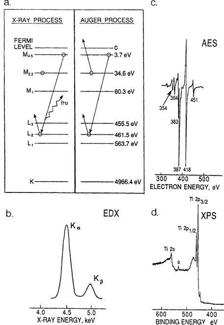
Figure 10-25 Electron excitation processes in Ti: (a) energy-level scheme; (b) EDX spectrum of Ti employing Si(Li) detector; (c) AES spectral lines for Ti (dN(E)/dE vs E); (d) a portion of the XPS spectrum for Ti (MgKα radiation).
where Z is the atomic number and n is the principal quantum number. For Ti (Z = 22), the calculated energy of the K shell (n = 1) is 6582 eV. Complex electron–electron interactions and shielding of the nucleus makes this formula far too simplistic for multielectron atoms. Both effects reduce electron binding energies relative to Eq. 10-20. Several of the prominent characteristic X-ray energies and wavelengths for Ti are:
Similarly, a prominent Ti Auger spectral transition is LMM or
A question that may have occurred to the reader at this point is, when do atoms with electron holes undergo X-ray transitions and when do they execute Auger processes? The answer is that both processes go on simultaneously. In the low-Z elements the probability is greater than an Auger transition will occur, whereas X-ray emission is favored for high-Z elements. The fractional probabilities of characteristic X-ray and Auger yields for KLM transitions, as well as electron binding energies of the elements, can be found in Ref. 35.
The variation of the principal characteristic X-ray and Auger lines with atomic number is shown in Figs. 10-26 and 10-27, respectively. Commercial spectrometers typically operate within the energy range spanned in these figures. Therefore, in EDX, K X-ray transitions are conveniently measured in low-Z materials while L series X-rays appear when high-Z elements are involved. Similarly, in AES, KLL and LMM transitions are involved for low-Z elements while LMM and MNN lines appear for high-Z elements. Although keeping track of the particular shell involved is sometimes annoying, spectra from virtually all of the elements in the periodic table can be detected with a single excitation source and a single detector. Fortunately, the resolution of X-ray or electron detectors is such that prominent lines of neighboring elements do not seriously overlap. This facilitates spectral interpretation and atomic fingerprinting.

Figure 10-26 Characteristic X-ray emission energies of the elements.
(Courtesy of Princeton Gamma Tech, Inc.)
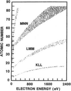
Figure 10-27 Principal Auger electron energies of elements.
(Courtesy of Physical Electronics Industries, Inc.)
The basis for understanding XPS lies in the same atomic core-electron scheme that we have been considering. Rather than incident electrons in the case of EDX and AES, relatively low-energy X-rays impinge on the specimen in this technique. The absorption of the photon results in the ejection of electrons via the photoelectric effect. Governing this process is the well-known but modified Einstein equation for the photoelectric effect expressed as
where EKE, hv, and EB are the energies of the ejected electron, the incident photon, and the involved bound electron state. Since values of the binding energy are element specific, atomic identification is possible through measurement of photoelectron energies.
10.4.3 X-RAY ENERGY DISPERSIVE ANALYSIS (EDX)
10.4.3.1 Equipment
Most X-ray energy dispersive analysis systems are interfaced to SEMs where the electron beam serves to excite characteristic X-rays from the probed area of the specimen. Attached to the SEM column is the liquid-nitrogen dewar with its cooled Si(Li) detector aimed to efficiently intercept emitted X-rays. The Si(Li) detector is a reverse biased Si diode doped with Li to create a wide depletion region. An incoming X-ray generates a photoelectron which eventually dissipates its energy by creating electron–hole pairs. The incident photon energy is linearly proportional to the number of pairs produced or equivalently proportional to the amplitude of the voltage pulse they generate when separated.
After the pulses are amplified they are sorted according to voltage amplitude by a multichannel analyzer which also counts and stores the number of pulses within given increments of the voltage (energy) range. The result is the characteristic X-ray spectrum shown for Ti in Fig. 10-25b. Si(Li) detectors typically have a resolution of about 150 eV so that overlap of peaks occurs when they are not separated in energy by more than this amount. Overlap sometimes occurs in multicomponent samples or when neighboring elements in the periodic table are present.
In an important variant known as X-ray wavelength dispersive analysis (WDX), wavelength rather than energy is dispersed, resulting in a factor of 20 or so improvement in X-ray linewidth resolution. In this case emitted X-rays, rather than entering a Si(Li) detector, are diffracted from single crystals with known interplanar spacings. From Bragg’s law, each characteristic wavelength reflects at corresponding angles which can be measured with very high precision. As the goniometer/detector assembly rotates, the peak is swept through as a function of angle. The electron microprobe (EMP) is an instrument specially designed to perform WDX analysis. This capability can also be achieved by attaching a diffractometer to an SEM column. The high spectral resolution of WDX is offset by its relatively slow speed of analysis.
10.4.3.2 Quantification
Quantitative analysis of an element in a multicomponent matrix is a complicated matter. The expected X-ray yield, YX(z), originating from some depth z below the surface depends on a number of factors: I0(z), the intensity of the electron beam at z; C, the atomic concentration; σ, the ionization cross section; ωχ, the X-ray yield; μ, the X-ray absorption coefficient; and ε, Ω, and θ, the detector efficiency, solid angle, and angle with respect to the beam, respectively. Therefore,
and the total signal detected is the sum contributed by all atomic species present integrated over the depth range. It is sometimes simpler to calibrate the yields against known composition standards. Excellent computer programs, both standardless and employing standards, are available for analysis and compositions are typically computed to approximately 0.1 at.%
10.4.4 AUGER ELECTRON SPECTROSCOPY (AES)
10.4.4.1 Equipment
The typical AES spectrometer, shown schematically in Fig. 10-28, is housed within an ultrahigh-vacuum chamber maintained at ∼ 10−10 torr. This level of cleanliness is required to prevent surface coverage by contaminants (e.g., C, O) in the system. The electron-gun source aims a finely focused beam of ∼ 2 keV electrons at the specimen surface, where it is scanned over the region of interest. Emitted Auger electrons are then energy analyzed by a cylindrical (or hemispherical in some systems) analyzer. This consists of coaxial metal cylinders (or hemispheres) raised to different potentials. The electron pass energy, E, is proportional to the voltage on the outer cylinder while the incremental energy range, ΔE, of transmitted electrons determines the resolution (ΔE/E), which is typically 0.2 to 0.5%. Electrons with higher or lower energies (velocities) than E hit either the outer or inner cylinders, respectively. They do not exit the analyzer and are not counted. By sweeping the bias potential on the analyzer, the entire electron spectrum is obtained. Auger electrons are but a part of the total electron yield, N(E), intermediate between low-energy secondary and high-energy elastically scattered electrons. They are barely discernible as small bumps above the background signal. Therefore, to accentuate the energy and magnitude of the Auger peaks, the spectrum is electronically differentiated and this gives rise to the common AES spectrum, or dN(E)/dE vs E response, shown in Fig. 10-25c for Ti. The reader should verify that differentiation of a Gaussian-like peak yields the wiggly narrow double peak response. By convention, the Auger line energy is taken at the resulting peak minimum.
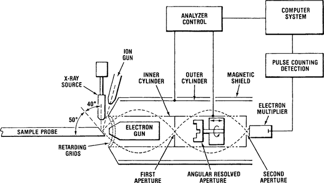
Figure 10-28 Schematic of spectrometer with combined AES and XPS capabilities.
(Courtesy of Physical Electronics Industries, Inc.)
Two very useful capabilities for thin-film analysis are depth profiling and lateral scanning. The first of these is accomplished with incorporated ion guns that enable the specimen surface to be continuously sputtered away while Auger electrons are being simultaneously detected. Multielement composition depth profiles can thus be determined over total film thicknesses of several thousand angstroms by sequentially sampling and analyzing arbitrarily thin layers. While depth resolution is extremely high, the frequently unknown sputter rates make precise depth determinations problematical. Through raster or line scanning of the electron beam, the AES is converted into an SEM and images of the surface topography are obtained. By modulating the imaging beam with the Auger electron signal, lateral composition mapping of the surface distribution of particular elements is achieved. Unlike EDX/SEM composition mapping, only the upper few atom layers are probed in this case.
Complete AES spectrometers are commercially available and often combined with XPS capabilities.
10.4.4.2 Quantification
The determination of the Auger electron yield from which atomic concentrations can be extracted is expressed by a formula similar in form to Eq. 10-22 for the X-ray yield. External standards are important in quantifying elemental analysis since standardless computer programs for AES are more imprecise than those for EDX analysis. A formula which has been widely used to determine the atomic concentration of a given species A in a multielement matrix is
The quantity Ii represents the intensity of the Auger line and is taken as the peak-to-peak span of the spectral line. Relative Auger sensitivities, Si, also enter Eq. 10-23. They have values ranging from 0.02 to 1 and depend on the element in question, the particular transition selected, and the electron-beam voltage. Uncertainties in C values so determined are perhaps a few at.%
10.4.5 X-RAY PHOTOELECTRON SPECTROSCOPY (XPS)
In order to capitalize on the X-ray-induced photoelectron effect, a spectrometer like the one used for AES (Fig. 10-28) is employed. The only difference is the excitation source, which is now a beam of either Mg or Al Kα X-rays. These characteristic X-rays have relatively low energy, e.g., hvMg = 1254 eV and hvA1 = 1487 eV, and set an upper bound to the kinetic energy of the detected photoelectrons.
A portion of the XPS spectrum for Ti is shown in Fig. 10-25d, where 2s, 2p1/2, and 2p3/2 peaks are evident. Interestingly, characteristic Auger electron transitions (not shown) frequently appear at precisely the energy locations indicated in Fig. 10-25c. The XPS peak positions, however, are shifted slightly by a few eV from those predicted by Eq. 10-21 because of the work function difference between specimen and detector.
It is beyond our scope to discuss spectral notation, the chemistry and physics of transitions, and the position and width of lines. What is significant is that linewidths are considerably narrower than those associated with Auger transitions. This fact makes it possible to gain useful chemical-bonding information which can also be obtained with less resolution by AES, but not by the other surface analytical techniques. It is for this reason that XPS is alternately known as ESCA (electron spectroscopy for chemical analysis).
Effects due to chemical bonding originate at the valence electrons and ripple beyond them to alter the energies of the core levels in inverse proportion to their proximity to the nucleus. As a result, energy shifts of a few eV occur and are resolvable. For example, in the case of pure Ti, the 2p3/2 line has a binding energy of 454 eV. In compounds this electron is more tightly bound to the Ti nucleus because electron charge clouds of the neighboring atoms "repel" it. In TiC, TiN, and TiO the same line is located at EB = 455 eV. Similarly, for the compounds TiO2, BaTiO3, PbTiO3, SrTiO3, CaTiO3, and (C2H5)2TiCl2 the transition occurs between EB = 458 and 459 eV. Clearly the magnitude of the chemical shift alone is not sufficient to establish the nature of the compound.
Aside from chemical bonding information, XPS has an important advantage relative to AES. X-rays are less prone to damage surfaces than electrons. For example, electron beams can reduce hydrocarbon contaminants to carbon, destroying the sought-after evidence. For this reason, XPS tends to be preferred in assessing the cleanliness of substrates and semiconductor films during MBE growth.
10.4.6 A COUPLE OF APPLICATIONS IN GAAS FILMS
10.4.6.1 AES
As an example of AES consider the depth profiles for Ga and Al shown in Fig. 10-29. The structure represents a single-crystal GaAs substrate onto which a 2000 Å thick, compositionally graded film of A1xGa1–xAs was grown by molecular beam epitaxy. At first the deposition rate of Al was increased linearly while that of Ga correspondingly decreased until AlAs formed; then the deposition rates were reversed until the GaAs composition was attained after 2000 Å. Finally, a 1000-Å cap film of GaAs was deposited resulting in a 2000-Å wide, V-shaped quantum well sandwiched between GaAs layers. Because the lattice constants of GaAs, AlAs, and the intermediate A1xGa1–xAs compositions differ by only 0.16% at most, the entire "lattice-matched" structure is free of crystallographic defects. During AES depth profiling, the film was sputtered away exposing surface compositions in reverse order to those which were initially deposited. The linearly graded walls of the quantum well reflect the precise control of deposition that is possible. In this case the values of SA1 and SGa are apparently independent of composition.
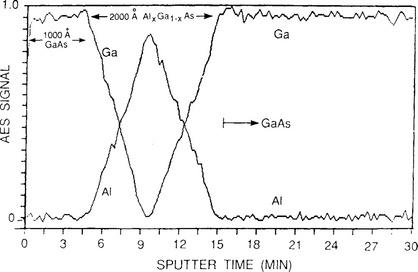
10.4.6.2 XPS
Here we consider an AlGaAs film that has been etched in a CF2Cl2 + O2 plasma in order to fabricate devices. It is desired to determine the composition of the film. But both electron-beam impingement and ion bombardment during sputter depth-profiling would alter or even remove surface compounds. What is needed is a technique to probe surface layers nondestructively. Angle-resolved XPS, based on altering the take-off angle for electron detection, is such a method. If the angle (0) exiting photoelectrons make with the surface plane is large, then chemical information on deep surface layers is sampled. However, if electrons exiting at a small grazing angle are detected, then only the top surface layers are probed; photoelectrons generated within deeper layers simply never emerge because their effective range (le) is smaller than the now-longer geometric escape-path length. In fact, the signal intensity from atoms at depth z varies as
In the analysis shown in Fig. 10-30, θ was varied from 90° to 20° while the Ga 3d peak was scanned. At the surface, bonding associated with GaF3 and Ga2O3 compounds was detected. Deeper within the film only Ga bound within GaAs or AlGaAs is evident.
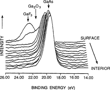
10.4.7 RUTHERFORD BACKSCATTERING (RBS)
10.4.7.1 Physical Principles
This popular thin-film characterization technique (Ref. 41) relies on the use of very high energy (MeV) beams of low-mass ions. These have the property of penetrating thousands of angstroms or even microns deep into films or film/substrate combinations. Interestingly, such beams cause negligible sputtering of surface atoms. Rather, the projectile ions lose their energy through electronic excitation and ionization of target atoms. These electronic collisions are so numerous that the energy loss can be considered to be continuous with depth. Sometimes the fast-moving light ions (usually 4He+) penetrate the atomic-electron-cloud shield and undergo close-impact collisions with the nuclei of the much heavier stationary target atoms. A resulting scattering from the Coulomb repulsion between ion and nucleus has been long known in nuclear physics as Rutherford scattering. A primary reason that this phenomenon has been so successfully capitalized upon for film analysis is that classical two-body elastic scattering is operative. This, perhaps, makes RBS the easiest of the analytical techniques to understand.
We start by first considering an ion of mass (atomic weight) M0 and energy E0 incident on a surface as shown in Fig. 10-31. An elastic collision between this ion and a surface atom of mass M occurs, such that afterward the ion energy is E1. The collision is insensitive to the electronic configuration or chemical bonding of target atoms, but depends solely on the masses and energies involved. As a consequence of conserving energy and momentum it is readily shown that
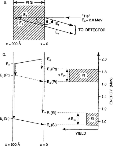
Figure 10-31 (a) Geometry of scattering and notation of energies at the front and back surfaces of a 900 Å thick PtSi film. (b) 4He+ ion energy as a function of film depth due to scattering from Pt and Si. Schematic RBS spectrum shown rotated by 90°.
(From W. K. Chu, J. W. Mayer, M. A. Nicolet, T. M. Buck, G. Amsel, and F. Eisen, Thin Solid Films 17, 1 (1963), with permission from Elsevier Sequoia S.A.)
where θ is the scattering angle. For a particular combination of M0, M, and θ the simple formula
relates the energy of emergent ions to that of the incident ions. KM is known as the kinematic factor and can be calculated from Eq. 10-24. Once the incident ion, e.g., 4He+ (M0 = 4) at E0 = 2 MeV, and angular position of the ion detector are selected (θ is typically 170°), KM just depends on the atomic weight of the target atom. For example, under the conditions just given, KPt = and KSi = 0.565. This means that if a 2 MeV He ion collides with a Pt atom (M = 195) located on the outer surface of a PtSi film, it will backscatter into the detector with an energy of 1.844 MeV; similarly, He ions scattering from surface Si atoms will have their energy reduced to 1.130 MeV.
Consider now what happens when a 2 MeV, 4He+ ion beam impinges on a 900 Å platinum silicide film on a Si wafer substrate. In Fig. 10-31a the film/substrate geometry is shown together with a schematic of the energy changes the ions undergo during nuclear scattering and the corresponding RBS spectrum (Fig. 10-31b). Energy changes (E0 → E1) for scattering from Pt and Si surface atoms are represented on the x = 0 axis. The majority of the He ions penetrate below the film surface, however, where they continuously lose energy at a linear rate (E0 → E2) with distance traversed. At any film depth they can suffer an atomic collision. The scattered ion energy is still given by Eq. 10-25, but E0 is now the incident He+ energy at that point in the matrix. Some of the energy-attenuated He+ ions can reach the PtSi/Si interface where they may backscatter (E3 = KME2) and again lose energy (E3 → E4) in traversing the film backward until they finally exit. Other He + ions can even penetrate the Si substrate where they eventually backscatter. It is important to realize that in the course of passage through the film, the ion beam can be thought of as splitting into two separate elemental components, each spanning a different range of energies. For each broad elemental peak detected, the highest and lowest energies correspond to atoms on the front and back film surfaces, respectively. Statistics largely govern the depth at which scattering occurs and whether Pt or Si atoms participate in the collisions.
Thus, by measuring the number and energy of backscattered He ions, information on the nature of the elements present, their concentration, and their depth distribution can all be simultaneously acquired without appreciably damaging the specimen.
10.4.7.2 Equipment
A schematic of the experimental arrangement employed for RBS is shown in Fig. 10-32. Lest the reader be deceived by the figure, it should be appreciated that the actual facility shown in the photograph of Fig. 10-33 is some 15 meters long and occupies more than 100 m2 of floor space. Ions for analysis, e.g., 4He+, 12C+, or 14N+, are accelerated at high voltages generated by the Van de Graaff accelerator. After entering the evacuated (˜ 10−6–10−7 torr) beam line, the ions are then collimated and focused. Ion mass selection occurs in the bending magnet which geometrically disperses ions according to their mass. The resultant ion beam is then raster-scanned across the surface of the specimen. Backscattered ions are analyzed with respect to their energy by a silicon surface-barrier detector capable of an energy resolution of ∼ 15 keV (peak width at half maximum amplitude). The electronic pulses are then amplified and sorted according to voltage amplitude, or energy, by a multichannel analyzer to yield the resulting RBS spectrum.
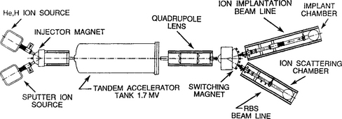
10.4.7.3 Elemental Information
All elements and their isotopes including Li and those above it in the periodic table are, in principle, detectable with 4He+ ions. The critical test is how well neighboring elements are resolved and this ultimately depends on the detector resolution. With 2 MeV 4He+ ions, isotopes with AM = 1 can generally be separated for M below approximately 40. At values of M ![]() 200 only atoms for which ΔM >20 can be resolved. Thus, 209Bi and 190 Os would be indistinguishable. The apparent advantage in separating low-Z elements is offset by their low cross sections (σi) for scattering. The σi are a measure of how efficiently target atoms scatter incoming ions and depend on Zi, particle energy E, the masses involved, and the angle of scattering. To a good approximation their dependence on these quantities for the two ions – (M0, Z0) and (M, Z)–involved varies as
200 only atoms for which ΔM >20 can be resolved. Thus, 209Bi and 190 Os would be indistinguishable. The apparent advantage in separating low-Z elements is offset by their low cross sections (σi) for scattering. The σi are a measure of how efficiently target atoms scatter incoming ions and depend on Zi, particle energy E, the masses involved, and the angle of scattering. To a good approximation their dependence on these quantities for the two ions – (M0, Z0) and (M, Z)–involved varies as
where the term in square brackets is an important correction for low-mass targets. Clearly, high-Z elements produce a stronger backscattered signal than low-Z elements.
Consideration of these factors suggest that specimens for RBS analysis should ideally contain elements of widely different atomic weight stacked with the heavy atoms near the surface and the lighter atoms below them. In bilayer film couples it is desirable for the high-M film to be at the outer surface. Otherwise there is the danger that elemental peaks will overlap. In general, when applicable, RBS can detect concentration levels of about 1 at.%. The technique is unmatched in determining the stoichiometry of thin-film binary compounds such as metal silicides where accuracies of ∼ ± 1% or so are achieved.
10.4.7.4 Spatial and Depth Resolution
Since MeV ion beams can only be focused to a spot size of a millimeter or so in diameter, the lateral spatial resolution of RBS is not great. The depth resolution is commonly quoted to be 200 Å but can be improved to 20 Å by altering the geometry of detection. Grazing exit angles are employed to make the film appear to be effectively thicker. For example, when θ = 95°, corresponding to an exit angle of 5°, ion scattering at a given film depth means that the energy loss path length is an order of magnitude longer. Implicit in the use of RBS is the desirability that the specimen surface and underlying layered structures be planar. Fortunately, polished Si wafers are extraordinarily flat. Films grown or deposited on Si maintain this planarity and are thus excellently suited for RBS analysis. Films with rough surfaces yield broadened RBS peaks.
The maximum film depth that can be probed depends on the ion used, its energy, and the nature of the matrix. Typically, ∼ 1 μm is an upper limit for 2 MeV 4He+ on Si. On the other hand, 3H+ beams of 2 MeV penetrate ∼ 5 μm deep.
10.4.7.5 Quantification
Despite the limitations noted earlier, RBS enjoys the status of being the preferred method of analysis in situations where it is applicable. The basic reasons are that it is quantitative from first principles, does not require elemental standards, and yields simultaneous depth and film thickness information. Clearly the area (A) under a spectral peak represents the total number of atoms of a given element present within the probed region or layer. The peak height (H) is directly proportional to the atomic concentration. Since the peak width (ΔE) is dependent on the maximum length traversed by projectile ions in the layer, ΔE is directly proportional to the layer or film thickness if the ion energy attenuation with distance is known. Particle range equations derived for nuclear physics applications yield this information to a high degree of accuracy. Hence, RBS provides a way to determine film thickness.
As an exercise in chemical analysis let us consider the experimental PtSi spectrum (Fig. 10-34) and calculate the relative proportions of Pt and Si present. By analogy to Eq. 10-23 the concentration ratio is given by
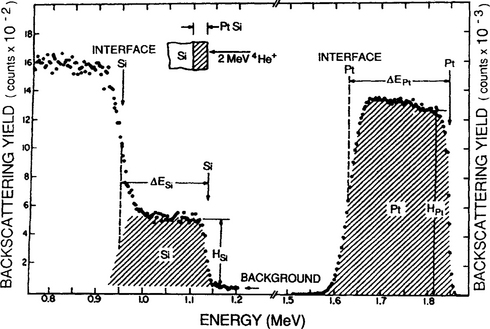
Figure 10-34 Energy spectrum for 2 MeV 4He+ ions backscattered from 900 Å of PtSi.
(From W. K. Chu, J. W. Mayer, M. A. Nicolet, T. M. Buck, G. Amsel, and F. Eisen, Thin Solid Films 17, 1 (1963), with permission from Elsevier Sequoia S.A.)
where Ai are the peak areas, and the scattering cross sections are, in effect, sensitivity factors. For PtSi, APt/ASi is measured to be 32, and σρ/σsi is estimated to be equal to (ZPt/ZSi)2 = 31.0, so that CPt/CSi = 1.03. Alternatively, since Ai = Hi ΔEi,
Experimental measurement reveals that Hpt/HSi = 27.5 and ΔEPt/ΔESi = 1.15, and therefore CPt/CSi is calculated to be 1.02.
Although film thickness can be determined to within 5%, the procedure is somewhat involved. The required ion energy loss with distance data, expressed as stopping cross sections, are tabulated and can be calculated for any matrix (Ref. 35). Film thicknesses can, in principle, also be determined either from known total incident charge and detector solid angle, or through the use of thickness standards. Experimental difficulties, however, limit the utility of these latter methods in practice.
10.4.7.6 Channeling
The role of channeling was already discussed in Section 4.6.4.2 in connection with development of preferred orientations during film growth under ion bombardment. A review of this section reveals how channeling effects might be advantageously used to distinguish RBS spectral features when crystalline (c), polycrystalline, and amorphous (a) film layers coexist. If, for example, an a-Si film covers c-Si, the higher 4He+ yield from a-Si will abruptly drop to the lower c-Si value at the a–c interface because of channeling in c-Si along certain crystallographic directions. During ion-implantation doping of semiconductors, channeling effects are unwelcome because dopant ions travel further, modifying their resulting profile in not easily predictable ways.
10.4.8 SECONDARY-ION MASS SPECTROMETRY (SIMS)
10.4.8.1 Physical Principles
The mass spectrometer, a common tool in the chemistry laboratory for the analysis of gases, has been dramatically transformed in recent years to create SIMS apparatus capable of analyzing the chemical composition of solid surface layers. A critical need to measure thermally diffused and ion-implanted depth profiles of dopants in semiconductor devices spurred the development of SIMS. In typical devices, peak dopant levels are about 1020/cm3 while background levels are ∼1015/cm3. These correspond to atomic concentrations in Si of 0.2% to 2 × 10⁻⁶%, respectively. None of the analytical techniques considered thus far has the capability of detecting such low concentration levels. The price paid for such high sensitivity is a complex spectrum of peaks that resembles Fig. 2-15, corresponding to the masses of detected ions and ion fragments. This necessitates the use of standards, composed of the specific elements and matrices in question, for quantitative determinations of composition.
In SIMS, a source of ions bombards the surface and sputters from its outermost film-layer neutral atoms, for the most part, but also positive and negative ions. Once in the gas phase, the ions are mass analyzed in order to identify the species present as well as determine their abundance. Since it is the secondary ion emission current which is detected in SIMS, high-sensitivity analysis requires methods for enhancing sputtered ion yields. Secondary-ion emission may be viewed as a special case of (neutral atom) sputtering. However, a comprehensive theory to quantitatively explain all aspects of secondary-ion emission (e.g., ion yields S+ or S−, escape velocities and angles, dependence on ion projectile and target material) does not yet exist. Reliable experiments to test proposed theories are difficult to perform. Experimentally, it has been found that different ion beams interact with the specimen surface in profoundly different ways. For example, the positive metal ion yield of an oxidized surface is typically enhanced tenfold and frequently more, relative to a clean surface. This accounts for the common practice of using O−2 beams to flood the surface when analyzing positive ions. Similarly, the negative ion signals can be enhanced by using Cs+ primary ion beams.
One of the theories which attempts to explain the opposing effects of O−2 and Cs+ beams involves charge transfer by electron tunneling between the target and ions leaving the target surface. Negative ion (O−2) bombardment repels charge from the surface, in effect lowering its Fermi energy and raising its effective work function (ϕ). Tunneling is now favored from the surface atom (soon to be an ejected positive ion) into the now-empty electron states of the target. Similarly, positive-ion (Cs+) bombardment lowers the target work function. Now electrons tunnel from the target into empty levels of surface atoms, enhancing the creation of negative ions. Since these charge transfer processes depend exponentially on ϕ, very large changes in ion yields with small shifts in ϕ are possible.
10.4.8.2 Instrumentation
A schematic depicting the basic elements of a conventional double-focusing SIMS spectrometer is shown in Fig. 10-35. The primary ions most frequently employed are Ar+, O−2, and Cs+, and these are focused into a beam with energy ranging from 2 to 15 keV. Sputtered charged atoms and compound fragments that are extracted enter an electrostatic energy analyzer similar to the cylindrical and spherical electron energy analyzers employed in AES and XPS work. Those secondary ions which pass now enter a magnetic-sector mass filter whose function is to select a particular mass for detection. The desired ion of mass M, charge q, and velocity ν traces an arc of radius r in the magnetic field (B) of the electromagnet, given by

Figure 10-35 Schematic of the ion optical system in the Cameca double-focusing mass spectrometer. 1, Cs ion source; 2, duoplasmatron source; 3, primary beam mass filter; 4, immersion lens; 5, specimen; 6, dynamic transfer system; 7, transfer optical system; 8, entrance slit; 9, electrostatic sector; 10, energy slit; 11, spectrometer lens; 12, spectrometer; 13, electromagnet; 14, exit slit; 15, projection lens; 16, projection display and detection system; 17, deflector; 18, channel plate; 19, fluorescent screen; 20, deflector; 21, Faraday cup; 22, electron multiplier.
(Courtesy Cameca Inc., Stamford, Connecticut.)
Two modes of operation are possible. In the imaging mode, B is fixed and simultaneous projection of ions of different mass on the channel plate yields mass spectra maps in the form of an ion micrograph (spectrography). In the mass spectrometry mode, B is scanned and each ion mass is sequentially detected by the electron-multiplier detector. Magnetic sector mass filters possess high resolution capability (M/ΔM ∼ 3000–20,000). Another common version of SIMS employs a quadrupole lens of lower resolution, i.e., M/ΔM ∼ 500.
A further distinction is made between what is known as "static" and "dynamic" SIMS. The issue which distinguishes them is the rate of specimen erosion relative to the time necessary to acquire data. Static SIMS requires that data be collected before the surface is appreciably modified by ion bombardment. It is well suited to surface analysis and the detection of contaminants such as hydrocarbons. Dynamic SIMS, on the other hand, implies that high sputtering rates are operative during measurement. This, of course, enables depth profiling of surface layers. Typical operating parameters for both static and dynamic SIMS are given in Table 10-5.
Table 10-5 Comparison between Static and Dynamic SIMS
| Variable | Static SIMS | Dynamic SIMS |
|---|---|---|
| Residual gas pressure (torr) | 10−9–10−10 | 10-7 |
| Primary ion energy (keV) | 0.5–3 | 3–20 |
| Current density (A/cm2) | 10−9–10-6 | 10−5–10−2 |
| Area of analysis (cm2) | 0.1 | 10-4 |
| Sputter rate (s/monolayer) | 104 | 1 |
10.4.8.3 Two Extraordinary Capabilities
Among the unique features of SIMS are the ability to discriminate between ions of different mass, and to quantitatively measure very shallow dopant profiles. The first capability often provides interesting processing information. For example, consider a bipolar transistor which contains both 121Sb and 123sb in the emitter but only 121Sb in the collector. The emitter doped with both naturally occurring isotopes of antimony must have been diffused while the collector was obviously ion implanted. Extreme discrimination is required when two species of very similar mass must be distinguished. For example, to separate the 31p (mass = 30.974) signal from the interfering 30SiH (mass = 30.982) background level, the resolution required is M/ΔM = 3872. With high-resolution mass spectrometers these species have been separated and phosphorous doping profiles obtained as shown in Fig. 10-36.
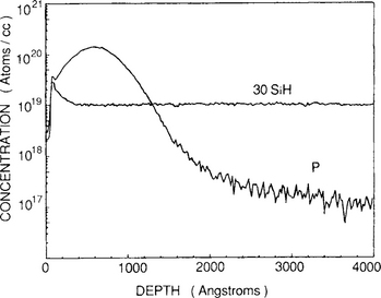
Figure 10-36 SIMS depth profile of P implanted in Si obtained with Cs+ ions.
(Courtesy of H. Luftman, AT&T Bell Laboratories.)
The second and more important capability is the critical detection and monitoring of dopant-ion implantation profiles in field-effect transistors. For this purpose primary ![]() ion beams are essential to enhance ionization efficiency. It is also important that the implant profile lie beneath or deeper than a surface transition region, a damaged layer where ion yields change continuously and quantification is problematical. However, once this layer is sputtered through and a steady state between incident and emitted primary ions occurs, constant secondary yields and accurate quantification are possible. When minimum feature dimensions were 0.25 μm or greater, i.e., prior to 1997, SIMS analysis encountered little difficulty because the implant profile lay deeper than the ∼ 10 to 30-nm thick surface transition region. In current 0.18 μm technology, a typical ultralow-energy dopant-ion implantation employs 500 eV boron with a projected range of only 3 nm. This means the transition region must be reduced to ∼ 0.1 to 0.4 nm, which is achievable with correspondingly low primary ion-beam energies. With such techniques the extremely shallow boron implant profile shown in Fig. 10-37 was characterized (Ref. 45).
ion beams are essential to enhance ionization efficiency. It is also important that the implant profile lie beneath or deeper than a surface transition region, a damaged layer where ion yields change continuously and quantification is problematical. However, once this layer is sputtered through and a steady state between incident and emitted primary ions occurs, constant secondary yields and accurate quantification are possible. When minimum feature dimensions were 0.25 μm or greater, i.e., prior to 1997, SIMS analysis encountered little difficulty because the implant profile lay deeper than the ∼ 10 to 30-nm thick surface transition region. In current 0.18 μm technology, a typical ultralow-energy dopant-ion implantation employs 500 eV boron with a projected range of only 3 nm. This means the transition region must be reduced to ∼ 0.1 to 0.4 nm, which is achievable with correspondingly low primary ion-beam energies. With such techniques the extremely shallow boron implant profile shown in Fig. 10-37 was characterized (Ref. 45).
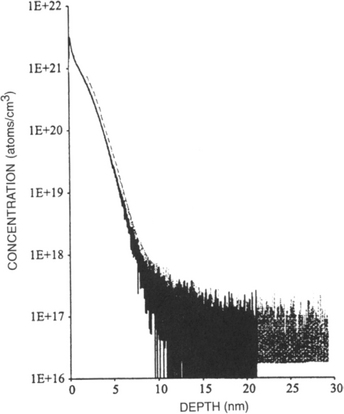
Figure 10-37 SIMS profiles of 1 keV BF2 in silicon with dose of 3.5 × 10¹⁴ atoms/cm2. Analytical conditions: (dotted gray) 310 eV ![]() primary ions, oblique incidence at 50° with oxygen flood; (solid black) 220 eV
primary ions, oblique incidence at 50° with oxygen flood; (solid black) 220 eV ![]() primary ions, normal incidence without oxygen flood.
primary ions, normal incidence without oxygen flood.
(From Ref. 45. Reprinted with the permission of Charles W. Magee.)
10.4.9 APPLICATIONS
The chapter closes with the self-explanatory Table 10-6 in which some applications of the surface analytical techniques just considered are listed. Varied phenomena, materials, and structures included extend into all facets of thin-film science and technology. Ever-expanding applications will ensure future growth of the list.
Table 10-6 Applications of Surface Analytical Techniques in Thin Films
| Application | Information obtained, comments | Technique |
|---|---|---|
| 1. Film nucleation, growth | Distinctions among island, layer, and S-K growth | AES |
| 2. Diffusion in films | Diffusion coefficients are obtained by sputter sectioning and surface accumulation methods | AES, SIMS, RBS |
| 3. Doped semiconductors | Diffused and ion-implanted depth profiles in Si and GaAs | SIMS |
| 4. Compound formation | Stoichiometry of intermetallic and silicide compounds, growth kinetics | RBS, AES |
| 5. Compound chemistry | Identification of valence and bonding state | XPS |
| 6. Investigation of surface residues, stains, haze, and discoloration | Identification of elemental contaminants, reliability and failure studies | AES, SIMS, XPS |
| 7. Contamination of surfaces by organic materials | Identification of elements Identification of compounds | AES, SIMS, XPS XPS |
| 8. Interfacial analysis | Cause of adhesion failure, segregation of impurities at grain boundaries and interfaces | AES, SIMS, XPS |
| 9. Multilayer films and coatings, superlattices | Stoichiometry, layer thickness, interfacial impurities | AES, RBS, SIMS |
| 10. Determination of crystalline perfection | Channeling spectra distinguish between single-crystal and amorphous Si films | RBS |
| 11. Fracture of coatings | Segregation of impurities at fracture surfaces | AES, SIMS |
| 12. Metal–semiconductor contacts | Adhesion, contact reactions in Si and GaAs | AES, XPS, SIMS, RBS |
| 13. Dielectric films on metals and semiconductor | Surface contamination, impurity diffusion, and segregation at interfaces (e.g., SiO2–Si) | AES, SIMS, XPS |
| 14. Molecular beam epitaxy | Assessment of surface cleanliness prior to deposition, detection of C and O contaminants | AES, XPS |
10.5 CONCLUSION
The emergence of characterization instrumentation with unprecedented measurement capabilities has helped fuel the remarkable advances we have witnessed in thin-film science and technology. This chapter has attempted to convey how the insatiable and seemingly insurmountable demands for precise monitoring, control, and measurement of film thickness, structure, and composition are accomplished. It is remarkable that such characterization has been made against a backdrop of shrinking film dimensions, the need to analyze multilayered film structures, and the necessity to make real-time measurements in film deposition and etching environments. Capitalizing on an infrastructure of advances in electronic and optical instrumentation, computer technology and software development, all film characterization capabilities have dramatically expanded in the past decade. For example, prior thin-film thickness determinations by both interferometry and ellipsometry were practically limited to a single film; extraction of n and k as a function of wavelength was very time consuming. Today commercial spectral reflectometers and ellipsometers enable measurements over a broad spectral range to greatly expand the optical information content; besides n and k values, dielectric multilayer stacks can be analyzed, and all in a relatively short time. Furthermore, a totally new photoacoustic technique based on picosecond ultrasonics enables the thickness of individual opaque (metal) films within stacks to be rapidly measured with good accuracy. In summary, it is now possible to nondestructively measure the thickness, characterize the surface roughness, and model subsurface defects in both individual dielectric and metal films and multilayers.
Microstructural and morphological characterization of films by TEM and SEM methods have been augmented in recent years by a host of scanning probe microscopies. Few structural secrets remain now that atomic-resolution imaging can be attained on film surfaces by the STM and AFM, as well as in the film interior and at interfaces with TEM plan and cross-sectional views. Compositional characterization of films relies either on the unique electronic structure or the mass of the elements. Fingerprinting atoms by AES and XPS methods capitalizes on the former, whereas SIMS and RBS are based on the latter. It is a desideratum in all of these techniques to be able to unambiguously identify elemental species, detect fewer atoms, reduce the lateral and depth dimensions being probed, and perform the resulting analysis in shorter time periods. Prime objectives are real-time compositional monitoring and control of thin-film processing where possible, and the extension of these capabilities to multilayers. These challenges are daunting and require the most sophisticated and costly instrumentation employed in film characterization.
1. The reflectance plotted in Fig. 10-2 has the mathematical form
where δ = 4πn1 d/λ, r1 = (n0-n1)/(n0 + n1) and r2 = (n1-n2)/(n1 + n2).
2. Consider a 4428 Å thick Nb2O5 film on a quartz substrate (n = 1.45). Plot the reflectivity of this combination using n(λ) values shown in Fig. 10-3b and the formula for R given in exercise 1. Note that this form of R is valid only when k = 0. How does the R response compare with that shown in Fig. 10-3a over the wavelength range 400–800 nm?
4. Model the vibrating quartz-crystal thickness monitor as a mass (m) – spring combination, where k is the spring constant.
5. After monitoring the thickness of a deposited Au film with a 6.0 MHz quartz (AT cut) crystal monitor, a researcher decides to confirm his results employing interferometry. A frequency shift of 10.22 Hz was recorded for the film measuring 1.00 cm2 in area. Interferometry with the Hg green line revealed a displacement of 1.75 fringes across the film step. Are these measurements consistent? If not, suggest plausible reasons why not. Note: Density of Au is 19.3 g/cm3.
6. Based on the diffraction pattern of Fig. 10-19, what are the lattice parameters for Ag and Pb? Note: λcυκα = 1.54 Å.
7. Explain how an SEM/EDX facility could be used to measure the thickness of a film without detaching it from substrate B (film thickness standards may be necessary). Can the film thickness be measured this way if film and substrate have the same composition?
8. Suppose the specimen–tip current in an STM is given by
where q is the electronic charge, h is Planck’s constant, ϕ is the work function of the tip metal, νT is the tip voltage, and m is the mass of the electron.
9. X-ray rocking curves for an epitaxial GalnAsP film lattice-matched to InP were recorded for the (002), (006), and (117) reflections using CuKα radiation.
10. The surface of a film contained the following elements with the indicated sensitivities, S, and Auger intensities, I (in arbitrary units)
| Element | S | I |
|---|---|---|
| Ga | 0.68 | 6,950 |
| As | 0.68 | 5,100 |
| Al | 0.23 | 3,040 |
| O | 0.71 | 26,900 |
| C | 0.30 | 5,000 |
| F | 1.0 | 40,500 |
| Cl | 0.89 | 3,700 |
11. Auger electrons emanating from A atoms located a depth z below the surface give rise to a signal of intensity
where λe is the electron escape depth, C(z) is the concentration of A atoms, and K is a constant.
12. A 2000-Å tungsten film is sputtered on a flat polycrystalline diamond substrate.
14. The implanted P dopant distribution shown in the SIMS spectrum of Fig. 10-36 can be described by Eq. 4-43.
15. Recommend specific structural (e.g., film thickness, topography) and chemical characterization (i.e., composition) techniques for analyzing the following samples. In each case indicate potential difficulties in the analysis.
1 Bindell J.B. Sze S.M., editor. VLSI Technology. New York: McGraw-Hill, 1988.
2 Pliskin W.A., Zanin S.J. Maissel L.I., Glang R. Handbook of Thin Films Technology. New York: McGraw-Hill, 1970.
3 Chopra K.L. Thin Film Phenomena. New York: McGraw-Hill; 1969.
4 Pulker H.K. Coatings on Glass, 2nd ed. Amsterdam: Elsevier, 1999.
5 Tolansky S. Multiple Beam Interference Microscopy of Metals. London: Academic Press; 1970.
6 Jackson J.D. Classical Electrodynamics, 3rd ed. New York: John Wiley & Sons, 1999.
7 Forouhi A.R., Bloomer I. Phys. Rev.. 1988;B38:1865.
8 Callegari A., Babich K. SPIE. 1997;3050:507.
9 Vedam K. Thin Solid Films. 1998;313–314:1.
10 Theeten J.B., Aspenes D.E. Ann. Rev. Mater. Sci.. 1981;11:97.
11 Irene E.A., Woollam J.A. MRS Bull.. 1995;XX:24.
12 Tompkins H.G. A User’s Guide to Ellipsometry. Boston: Academic Press; 1993.
13 Jenkins T.E. J. Phys. D: Appl. Phys.. 1999;32:R45.
14 McMarr P.J., Vedam K., Narayan J. J. Appl. Phys.. 1986;59:694.
15 Jan/FebBallinger C.T., Olds R. Vacuum Coating Technoi. 2000:33.
16 Glang R. Maissel L.I., Glang R. Handbook of Thin-Film Technology. New York: McGraw-Hill, 1970.
17 JuneMorath C.J., Collins G.J., Wolf R.G., Stoner R.J. Solid State Technology. 1997.
18 DeJule R., Semicond. Int. 1998;5(21):52. same issue. DeJule R. Semicond. Int.. 1998;21(5):48.
19 Ohring M. Reliability and Failure of Electronic Materials and Devices. Boston: Academic Press; 1998.
20 Stoner R.J., Morath C.J., Tas G., Sengupta S., Merchant S.M., Bindell J.B., Maris H.J. Proc. SPIE. 1998;3269:104.
21 Goldstein J.I., Newbury D.E., Echlin P., Joy D.C., Ronig A.D., Lyman C.E., Fiori C., Lifshin E. Scanning Electron Microscopy and X-Ray Micro analysis, 2nd ed. New York: Plenum, 1992.
22 Newbury D.E., Joy D.C., Echlin P., Fiori C.E. Advanced Scanning Electron Microscopy and X-Ray Micro analysis. New York: Plenum; 1986.
23 Thomas G., Goringe M.J. Transmission Electron Microscopy of Materials. New York: J. Wiley & Sons; 1979.
24 Williams D.B., Carter C.B. Transmission Electron Microscopy – A Textbook for Materials Science. New York: Plenum; 1996.
25 Ishitani T., Yaguchi T., Koike H. Hitachi Rev.. 1996;45(1):19.
26 2nd ed. Wiesendanger R., Guntherodt H.-J. Scanning Tunneling Microscopy. Heidelberg: Springer-Verlag, 1995. II
27 Kubby J.A., Boland J.J. Surf. Sci. Rep.. 1996;26:61.
28 Howland R., Benatar L. A Practical Guide to Scanning Probe Microscopy. Park Scientific Instruments; 1996.
29 Woodruff D.P., Delchar T.A. Modern Techniques of Surface Science. Cambridge: Cambridge University Press; 1994.
30 Nakayama T., Huang D.-H., Aono M. Microelectron. Eng.. 1996;32:191.
31 Crommie M.F., Lutz C.P., Eigler D.M. Science. 1993;262:218.
32 Ohring M. The Materials Science of Thin Films. Boston: Academic Press; 1991.
33 Binnig G., Quate C.F., Gerber C. Phys. Rev. Lett.. 1986;56:930.
34 Kitamura S., Iwatsuki M., Kitamura S., Suzuki K., Jpn. J. Appl. Phys. 1995;34:L145. Iwatsuki M. JEOL News. 1996;32E(1):42.
35 Feldman L.C., Mayer J.W. Fundamentals of Surface and Thin-Film Analysis. New York: North-Holland; 1986.
36 Riviere J.C. Surface Analysis Techniques. London: Oxford University Press; 1990.
37 Wachtman J.B. Characterization of Materials. Boston: Butterworth-Heinemann; 1993.
38 Briggs D., Seah M.P. Practical Surface Analysis by Auger and X-Ray Photoelectron Spectroscopy. Chichester, U.K.: J. Wiley & Sons, 1983.
39 Brundle C.R., Baker A.J., editors. Electron Spectroscopy: Theory, Techniques, and Applications, Vol. I-X. New York: Academic Press, 1979.
40 Watts J.F. An Introduction to Surface Analysis by Electron Spectroscopy. London: Oxford University Press; 1990.
41 Bird J.R., Williams J.S. Ion Beams for Materials Analysis. Sydney: Academic Press, 1989.
42 Wilson R.G., Stevie F.A., Magee C.W. Secondary Ion Mass Spectrometry. New York: J. Wiley & Sons; 1989.
43 Benninghoven A.W., Rudenauer F.G., Werner H.W. Secondary Ion Mass-Spectrometry–Basic Concepts, Instrumental Aspects, Applications and Trends. New York: J. Wiley & Sons; 1987.
44 Werner H.W., Garten P.P.H. Rep. Prog. Phys.. 1984;47:221.
45 Chia V.K.F., Mount G.R., Edgell M.J., Magee C.W. J. Vac. Sci. Technol.. 1999;B17:2345.