
Chapter 4 Discharges, Plasmas, and Ion–Surface Interactions
4.1 INTRODUCTION
Evaporation caused by absorption of thermal energy is not the only way to induce atoms to leave a liquid or solid surface. Atoms can also be ejected or sputtered from solids at room temperature by bombarding their surfaces with energetic ions. In either case the emitted atoms traverse a reduced pressure ambient and deposit atomistically on a substrate to form a film. Because physical means are primarily involved in producing films, both are known as physical vapor-deposition (PVD) processes. Despite some superficial similarities, it is immediately apparent that evaporation and sputtering are quite different if we consider Fig. 4-1a depicting a simplified sputtering system capable of depositing metals films. Inside is a pair of parallel metal electrodes, one of which is the cathode or target of the metal to be deposited. It is connected to the negative terminal of a DC power supply and typically, several kilovolts are applied to it. Facing the cathode is the substrate or anode, which may be grounded, biased positively or negatively, heated, cooled, or some combination of these. After evacuation of the chamber, a working gas, typically argon, is introduced and serves as the medium in which an electrical discharge is initiated and sustained. Gas pressures usually range from a few to a hundred millitorr. After a visible glow discharge is maintained between the electrodes, it is observed that a current flows, and metal from the cathode deposits on the substrate.

Microscopically, positive gas ions in the discharge strike the cathode and physically eject or sputter target atoms through momentum transfer to them. These atoms enter and pass through the discharge region to eventually deposit on the growing film. In addition, other particles (secondary electrons, desorbed gases, and negative ions) as well as radiation (X-rays and photons) are emitted from the target. The electric field accelerates electrons and negatively charged ions toward the anode substrate where they impinge on the growing film. An ionized gas or plasma rather than a vacuum environment, active electrodes that participate in the deposition process, and low-temperature processing are among the features that distinguish sputtering from evaporation. From this simple description, it is quite clear that compared to the predictable rarefied-gas behavior in an evaporation system, the glow-discharge plasma is a very busy and not easily modeled environment. Similar effects occur even when the electrodes are AC powered as shown in Fig. 4-1b.
In the past few decades, advances in our understanding of the physics and chemistry of ionized gases has led to the widespread adoption of plasma technology for the deposition and removal (etching) of thin films as well as the modification of surfaces in a diverse variety of technologies. Microelectronics applications have been the main technological driver in this regard; presently, upward of a third of integrated circuit fabrication steps are associated with the use of plasmas. In addition, there are critical plasma processing operations in the automotive, optical coating, biomedical, information recording, waste management, and aerospace industries.
Regardless of the plasma process, however, roughly similar discharges, electrode configurations, and gas/solid interactions are involved. The purpose of this chapter is to introduce fundamental scientific issues common to all glow discharge systems. These include topics related to initiating and sustaining discharges, the dynamical behavior of the charged and neutral species, and their interactions within the plasma. Both inert gas discharges and the more complex chemically reactive plasmas will be discussed in this regard. Ion interactions with the cathode and film or substrate surfaces are particularly important in plasma processing. Therefore, coverage of the fundamental physics of sputtering and ion-induced modification of growing films rounds out this chapter. Practical engineering issues related to the deposition and etching of metal and insulator films and descriptions of assorted plasma PVD and ion-beam processes are the subjects of the next chapter. Our treatment of plasma processing does not end then, but continues in Chapter 6 with a discussion of plasma-assisted chemical vapor deposition processes.
4.2 PLASMAS, DISCHARGES, AND ARCS
4.2.1 PLASMAS
The term plasma was apparently coined by Irving Langmuir in 1929 (Ref. 1) to describe the behavior of ionized gases in high-current vacuum tubes. It was soon realized that plasmas exhibited a behavior different from simple ideal (or nonideal) un-ionized gases, and were obviously distinct from condensed liquid and solid states of matter. For these reasons plasmas were termed a rare fourth state of matter. On a cosmic scale, however, considering the northern lights, stars, and interstellar hydrogen, it has been claimed that 99% of matter in the universe exists in plasma form; on this basis solids and liquids are actually the rare states of matter. Science fiction movies containing spectacular lightning discharges and glittering advertising signs employing neon lighting provided early vehicles for displaying the mysterious attributes of plasmas. Nitriding of steel surfaces in order to harden them, and fluorescent lighting based on mercury discharges, were among the early widespread applications capitalizing on this strange state of matter.
A plasma may be broadly defined as aquasineutral gas that exhibits a collective behavior in the presence of applied electromagnetic fields. Plasmas are weakly ionized gases consisting of a collection of electrons, ions, and neutral atomic and molecular species. This definition is broad enough to encompass the spectrum of space and man-made plasmas extending from stars, solar winds and coronas, and the earth’s ionosphere to the regime of high-pressure arcs, shock tubes, and fusion reactors. These space and laboratory created plasmas broadly differ in the density n(number per cm3) of charged species. In the former rarified environments, n is typically less than 107cm−3, whereas experimentally, densities approaching 1020 cm−3 in magnitude have been realized in the latter man-made high-pressure plasmas. In between these extremes are the glow discharges and arcs with which this book is primarily concerned. These plasmas with ion densities ranging from ∼ 108 cm−3 to ∼1014 cm−3 are the ones exploited in the industrial plasma-processing applications we shall consider.
4.2.2 THE TOWNSEND DISCHARGE
We have seen that application of a sufficiently high DC voltage between metal electrodes immersed in a low-pressure gas initiates a discharge. What is the mechanism that converts the initially insulating gas into an electrically conducting medium? This is the first question that must be addressed in order to understand the nature of such gaseous conducting media or plasmas. In essence, the discharge reflects a gaseous breakdown that may be viewed as the analog of dielectric breakdown in insulating solids; there dielectrics conduct electricity at critical applied voltages. In gases the process begins when a stray electron near the cathode carrying an initial current i0 is accelerated toward the anode by the applied electric field (![]() ). After gaining sufficient energy the electron collides with a neutral gas atom (A) converting it into a positively charged ion (A+). During this impact ionization process, charge conservation indicates that two electrons are released, i.e.,
). After gaining sufficient energy the electron collides with a neutral gas atom (A) converting it into a positively charged ion (A+). During this impact ionization process, charge conservation indicates that two electrons are released, i.e.,
These are accelerated and now bombard two additional neutral gas atoms, generating more ions and electrons, and so on. Meanwhile, the electric field drives ions in the opposite direction where they collide with the cathode, ejecting, among other particles, secondary electrons. These now also undergo charge multiplication. The effect snowballs until a sufficiently large avalanche current ultimately causes the gas to breakdown.
In order for breakdown to occur, the distance (d) between electrodes must be large enough to allow electrons to incrementally gain the requisite energy for an ionization cascade. Also, the electrodes must be wide enough to prevent the loss of electrons or ions through sideways diffusion out of the interelectrode space. The Townsend equation, whose derivation will be left for the reader in Exercise 1, is written as
This equation reveals that the discharge current (i) rises dramatically from i0 because of the combined effects of impact ionization and secondary-electron generation. These processes are respectively defined by constants α and γe. Known as the Townsend ionization coefficient, α represents the probability per unit length of ionization occurring during an electron-gas atom collision. Quantity γe is the Townsend secondary-electron emission coefficient and is defined as the number of secondary electrons emitted at the cathode per incident ion. For an electron of chargeq traveling a distance λ, the probability of reaching the ionization potential Vi is exp — (Vi/q![]() λ), so that
λ), so that
We may associate λ with the intercollision distance or mean free path in a gas. Since Eq. 2-5 reveals that λ ∼ P−1, we expect α to be a function of the system pressure.
Breakdown is assumed to occur when the denominator in Eq. 4-2 is equal to zero, i.e., γe(exp αd − 1) = 1, for then the current is infinite. From this condition plus Eqs. 4-3 and 2-5, the critical breakdown field ![]() and voltage
and voltage ![]() can be calculated with a bit of algebra and expressed in terms of a product of pressure and interelectrode spacing. The result, known as Paschen’s Law, is expressed by
can be calculated with a bit of algebra and expressed in terms of a product of pressure and interelectrode spacing. The result, known as Paschen’s Law, is expressed by
where A and B are constants.
The Paschen curve, a plot of VB vs Pd, is shown in Fig. 4-2 for a number of gases. At low values of Pd there are few electron–ion collisions and the secondary electron yield is too low to sustain ionization in the discharge. On the other hand, at high pressures there are frequent collisions, and since electrons do not acquire sufficient energy to ionize gas atoms, the discharge is quenched. Thus at either extreme, ion generation rates are low and high voltages are required to sustain the discharge. In between, at typically a few hundred to a thousand volts, the discharge is self-sustaining. This means that for each electron at the cathode, exp(αd) electrons reach the anode, and the net effect of the collisions is to produce a new electron at the cathode. Practically, however, in most sputtering discharges the Pd product is well to the left of the minimum value.

4.2.3 TYPES AND STRUCTURES OF DISCHARGES
It is instructive to follow the progress of a glow discharge in a low-pressure gas using a high-impedance DC power supply (Ref. 2). In the regime just considered, known as the Townsend discharge, a tiny current flows initially due to the small number of charge carriers in the system. With charge multiplication, the current increases rapidly, but the voltage, limited by the output impedance of the power supply, remains constant. Eventually, when enough electrons produce sufficient ions to regenerate the same number of initial electrons, the discharge becomes self-sustaining. The gas begins to glow now and the voltage drops accompanied by a sharp rise in current. At this point normal glow occurs. Initially, ion bombardment of the cathode is not uniform but concentrated near the cathode edges or at other surface irregularities. As more power is applied, the bombardment increasingly spreads over the entire surface until a nearly uniform current density is achieved. A further increase in power results in both higher voltage and cathode current-density levels. The abnormal discharge regime has now been entered and this is the operative domain for sputtering and other discharge processes such as plasma etching.
At still higher currents, the cathode gets hotter. Now thermionic emission of electrons exceeds that of secondary-electron emission and low-voltage arcs propagate. Arcs have been defined (Ref. 3) as gas or vapor discharges where the cathode voltage drop is of the order of the minimum ionizing or excitation potential. Furthermore, the arc is a self-sustained discharge that supports high currents by providing its own mechanism for electron emission from negative or positive electrodes. A number of commercial PVD processes rely on arcs. This subject will therefore be deferred to the end of Chapter 5 so that the intervening treatment of plasma physics and processing can form the basis for a discussion of these arc-deposition methods.
Returning to the DC discharge we note that there is a progression of alternating dark and luminous regions between the cathode and anode, as shown in Fig. 4-3. Although the general structure of the discharge has been known for a long time the microscopic details of charge distributions, behavior, and interactions within these regions are not totally understood. The Aston dark space is very thin and contains both low energy electrons and high energy positive ions, each moving in opposite directions. Beyond it thecathode glow appears as a highly luminous layer that envelops and clings to the cathode. De-excitation of positive ions through neutralization is the probable mechanism of light emission here.

Figure 4-3 Structure of a DC glow discharge with corresponding potential, electric field, charge, and current distributions.
Next to appear is the important Crookes or cathode dark space where some electrons are energized to the point where they begin to impact-ionize neutrals; other lower energy electrons impact neutrals without ion production. Because there is relatively little ionization this region is dark. Most of the discharge voltage is dropped across the cathode dark space, also commonly referred to as the cathode sheath. The resulting electric field serves to accelerate ions toward their eventual collision with the cathode. Next in line is the negative glow. Here the visible emission is apparently due to interactions between assorted secondary electrons and neutrals with attendant excitation and de-excitation. Beyond lie the Faraday dark space, the positive column, and finally the anode. During sputtering the substrate is typically placed inside the negative glow before the Faraday dark space so that the latter as well as the positive column do not normally appear.
When a DC voltage V is applied between the anode and cathode the electric potential distribution, unlike the case for a simple vacuum capacitor, is highly nonlinear with distance x; similarly, the electric field ![]() is not constant. Furthermore, the deviations are most pronounced near the electrodes. These characteristics stem from the complex distribution of charge near electrodes and within the plasma, and the resultant currents they produce. After considering aspects of plasma physics contained in Section 4.3, some causes of these puzzling electrical responses may, hopefully, be clarified.
is not constant. Furthermore, the deviations are most pronounced near the electrodes. These characteristics stem from the complex distribution of charge near electrodes and within the plasma, and the resultant currents they produce. After considering aspects of plasma physics contained in Section 4.3, some causes of these puzzling electrical responses may, hopefully, be clarified.
4.3 FUNDAMENTALS OF PLASMA PHYSICS
In this section readers will find a concise treatment of several important issues related to plasmas and their interaction with surfaces placed in their midst. The discussion here is largely distilled from the more complete treatments of the subject that can be found in the readily accessible books by Chapman (Ref. 4), Grill (Ref. 5), Mahan (Ref. 6), and Lieberman and Lichtenberg (Ref. 7). They are all recommended for their integration of the fundamental principles of glow-discharge plasmas in applications to thin-film processing.
4.3.1 PLASMA SPECIES
Let us now consider the interior of the plasma, i.e., a partially ionized gas composed of respective densities of electrons (ne), ions (ni), and neutral gas species (n0). Electrons and ions have more or less independent velocity distributions with electrons possessing far higher velocities than ions. The plasma is electrically neutral when averaged over all the particles contained within so that ne = ni = n. Collisions between neutral gas species essentially cause them to execute random Brownian motion. However, the applied electric field disrupts this haphazard motion because of ionization. If the density of charged particles is high enough compared with the dimensions of the plasma, significant coulombic interaction exists among particles. This interaction enables the charged species to flow in a fluid-like fashion that determines many of the plasma properties.
The degree of gas ionization (fi) is defined by
and typically has a magnitude of ∼ 10−4 in the glow discharges used in thin-film processing. Therefore, at pressures of ∼ 10 millitorr, Fig. 2-2 based on the ideal gas law indicates a gas density of n0 ∼ 1014 cm−3; hence the electron and ion densities will be about 1010 cm−3 each at 25°C. In high density plasmas, fi can reach 10−2 and charge densities more than 1012 cm−3.
4.3.2 PARTICLE ENERGIES AND TEMPERATURES
Measurements on glow discharges yield electron energies (Ee) that span the range 1 to 10 eVwith 2 eV being a typical average value for calculation purposes. The effective or characteristic temperature T associated with a given energy E is simply given by T = E/kB, where kB is the Boltzmann constant. Substituting Ee=2 eV, we find that electrons have an astoundingly high temperature Te of some 23,000 K. However, because there are so few of them, their heat content is small and the chamber walls do not heat appreciably. Neutral gas atoms or molecules and ions are far less energetic; the former have energies of only 0.025 eV (or T0 = 293 K) and the latter, energies of ∼ 0.04 eV (orTi = 500 K). Ions have higher energies than neutrals because they acquire energy from theapplied electric field.
In addition, there may be excited species at temperature Tex with energy Eex. Neutral molecules may become excited by virtue of acquired energy that is partitioned into translational as well as internal vibrational and rotational modes of motion; for each of these modes there is a corresponding characteristic temperature. For example, in a nitrogen gas plasma at several torr, Te may be over 12,000 K and T0 due to molecular translation is ∼ 1000 K, while equivalent temperatures for vibrational (Tv) and rotational (Tro) modes are ∼3800 K and 2800 K, respectively (Ref. 7). Higher plasma pressures tend to narrow this overall disparity in temperature.
Thermodynamic equilibrium in the system implies that all of the temperatures are equilibrated, i.e., Te = T0 = Ti = Tex = Tr = Tw, where Tr and Tw are the radiation and chamber wall temperatures, respectively. Since this condition is never met in our low-pressure glow discharges, we speak of a nonequilibrium or cold plasma. Plasmas types are often differentiated on the basis of the electron energy and temperature. For example, Te for glow discharges is greater than that for flames but considerably less than that for fusion plasmas.
4.3.3 MOTION OF PLASMA SPECIES: CURRENTS AND DIFFUSION
Since surfaces (e.g., targets, substrates) are immersed in the plasma, they are bombarded by the species present. Simple kinetic theory of gases helps us understand what happens. The neutral particle flux can be calculated from Eq. 2-8. Unlike neutrals however, charged particle impingement results in an effective electrical current density (j) given by the product of the particle flux (![]() ) and the charge (q) transported, where the factor of
) and the charge (q) transported, where the factor of ![]() reflects that fraction of the random motion that is directed at the planar surface. Therefore,
reflects that fraction of the random motion that is directed at the planar surface. Therefore,
where n and ![]() are the charged species concentration and mean velocity. To compare the behavior of different species we take
are the charged species concentration and mean velocity. To compare the behavior of different species we take ![]() (Eq. 2-3b). In the case of electrons, me = 9.1 × 10⁻²⁸ g, and if we assumeTe = 23,000K,υe = 9.5 × 107 cm/s; similarly, for typical Ar ions υi = 5.2 × 104 cm/s. Furthermore, if ne = ni = 1010/3, je ∼ 38 mA/cm2 and ji = 21μA/cm2. The implication of this simple calculation is that an isolated surface within the plasma charges negatively initially because of the greater electron bombardment. Subsequently, additional electrons are repelled while positive ions are attracted. Therefore, the surface continues to charge negatively at a decreasing rate until the electron flux equals the ion flux and there is no net current.
(Eq. 2-3b). In the case of electrons, me = 9.1 × 10⁻²⁸ g, and if we assumeTe = 23,000K,υe = 9.5 × 107 cm/s; similarly, for typical Ar ions υi = 5.2 × 104 cm/s. Furthermore, if ne = ni = 1010/3, je ∼ 38 mA/cm2 and ji = 21μA/cm2. The implication of this simple calculation is that an isolated surface within the plasma charges negatively initially because of the greater electron bombardment. Subsequently, additional electrons are repelled while positive ions are attracted. Therefore, the surface continues to charge negatively at a decreasing rate until the electron flux equals the ion flux and there is no net current.
We now consider the mobility (μ) of charged species in the presence of an applied electric field ![]() . The mobility is defined as the velocity per unit electric field or
. The mobility is defined as the velocity per unit electric field or ![]() . Using Newton’s law,
. Using Newton’s law,
where q isthe species charge. The second term on the right reflects a kind of frictional drag particles experience during motion because of their collisions with other particles. When the particle collides, it essentially loses its directed motion. It is common to set [δυ/δt]coll = υν, where ν is the collision frequency, a factor assumed for simplicity to be constant. In the steady state, dv/dt = 0 and ![]() . Typical mobilities for gaseous ions at 1 torr and 273 K range from ∼4 × 102 cm2/V-s (for Xe+) to 1.1 × 104 cm2/V-s (for H+).
. Typical mobilities for gaseous ions at 1 torr and 273 K range from ∼4 × 102 cm2/V-s (for Xe+) to 1.1 × 104 cm2/V-s (for H+).
A second kinetic effect involving species motion in plasmas is diffusion, a phenomenon governed by Fick’s Law (Eq. 1-22). When migrating species move under the simultaneous influence of two driving forces, i.e., diffusion in a concentration gradient (dn/dx) and drift in the applied electric field, we may write for the respective electron and ion particle fluxes,
To maintain charge neutrality in the region under consideration it is assumed that Je = Ji = J, and ne = ni = n. By equating Eqs. 4-8 and 4-9,
Therefore, it is apparent that an electric field develops because the difference in electron and ion diffusivities produces a separation of charge. Physically, more electrons than ions tend to leave the plasma, establishing an electric field that hinders further electron loss but at the same time enhances ion motion. Because of the coupled electron and ion motions we can assign (see Exercise 2) an effective ambipolar diffusion coefficient Da to describe the effect, i.e.,
The magnitude of Da lies somewhere between those ofDi and De so that both ions and electrons diffuse faster than intrinsic ions do.
4.3.4 ELECTRON MOTION IN COMBINED ELECTRIC AND MAGNETIC FIELDS
4.3.4.1 Parallel Fields
Let us now examine what happens when a magnetic field of strength B is superimposed parallel to the electric field ![]() between the target and substrate. Charged particles within the dual field environment experience the well-known Lorentz force in addition to electric field force, i.e.,
between the target and substrate. Charged particles within the dual field environment experience the well-known Lorentz force in addition to electric field force, i.e.,
where q, m, and υ are the electron charge, mass, and velocity, respectively. First consider the case where B and ![]() are parallel as shown in Fig. 4-4a. Only electrons will be considered because as we have already seen, their dynamical behavior controls glow-discharge processes. When electrons are emitted exactly normal to the target surface or parallel to both B and
are parallel as shown in Fig. 4-4a. Only electrons will be considered because as we have already seen, their dynamical behavior controls glow-discharge processes. When electrons are emitted exactly normal to the target surface or parallel to both B and ![]() , then υ × B vanishes; electrons are only influenced by the
, then υ × B vanishes; electrons are only influenced by the ![]() field and simply accelerate toward the anode, gaining kinetic energy in the process. If, however,
field and simply accelerate toward the anode, gaining kinetic energy in the process. If, however,![]() , and the electron is launched with velocity υ at an angle θ with respect to the uniform B field between electrodes (Fig. 4-4b), it experiences a force qυBsinθ in a direction perpendicular to B. The electron now executes a circular motion whose radius r is determined by a balance of the centrifugal (m(υsinθ)2/r) and Lorentz forces involved, i.e.,
, and the electron is launched with velocity υ at an angle θ with respect to the uniform B field between electrodes (Fig. 4-4b), it experiences a force qυBsinθ in a direction perpendicular to B. The electron now executes a circular motion whose radius r is determined by a balance of the centrifugal (m(υsinθ)2/r) and Lorentz forces involved, i.e.,

Figure 4-4 Effect of ![]() and B on electron motion. (a) Linear electron trajectory when
and B on electron motion. (a) Linear electron trajectory when ![]() . (b) Helical orbit of constant pitch when B ≠0,
. (b) Helical orbit of constant pitch when B ≠0, ![]() . (c) Helical orbit of variable pitch when
. (c) Helical orbit of variable pitch when ![]() . (d) Cycloidal electron motion on cathode when
. (d) Cycloidal electron motion on cathode when ![]() .
.
A spiral electron motion ensues and in corkscrew fashion the electron returns to the same radial position around the axis of the field lines. If the magnetic field were not present, such off-axis electrons would tend to migrate out of the discharge and be lost at the walls.
The case where electrons are launched at an angle to parallel and uniform ![]() and B fields is somewhat more complex (Fig. 4-4c). Helical motion with constant radius occurs, but because of electron acceleration in the
and B fields is somewhat more complex (Fig. 4-4c). Helical motion with constant radius occurs, but because of electron acceleration in the ![]() field the pitch of the helix lengthens with time. Time-varying fields complicate matters further and electron spirals of variable radius can occur. Clearly magnetic fields prolong the electron residence time in the discharge and enhance the probability of ion collisions.
field the pitch of the helix lengthens with time. Time-varying fields complicate matters further and electron spirals of variable radius can occur. Clearly magnetic fields prolong the electron residence time in the discharge and enhance the probability of ion collisions.
4.3.4.2 Perpendicular Fields
Through the application of perpendicular electric and magnetic fields even greater electron confinement is achieved. The geometry is shown in Fig. 4-4d, where ![]() is still normal to the cathode while B, which is directed into the page (+z direction), lies parallel to the cathode plane. Electrons emitted normally from the cathode ideally do not even reach the anode but are trapped near the electrode where they execute a periodic hopping motion over its surface. Physically, the emitted electrons are initially accelerated toward the anode, executing a helical motion in the process; but when they encounter the region of the parallel magnetic field, they are bent in an orbit back to the target in very much the same way that electrons are deflected toward the hearth in an e-gun evaporator. The analysis for this behavior is not difficult and starts with the equations for electron motion in the three perpendicular directions. Coordinate positions of the electron above and along the cathode are y and x, respectively. Applying the Lorentz equation we have
is still normal to the cathode while B, which is directed into the page (+z direction), lies parallel to the cathode plane. Electrons emitted normally from the cathode ideally do not even reach the anode but are trapped near the electrode where they execute a periodic hopping motion over its surface. Physically, the emitted electrons are initially accelerated toward the anode, executing a helical motion in the process; but when they encounter the region of the parallel magnetic field, they are bent in an orbit back to the target in very much the same way that electrons are deflected toward the hearth in an e-gun evaporator. The analysis for this behavior is not difficult and starts with the equations for electron motion in the three perpendicular directions. Coordinate positions of the electron above and along the cathode are y and x, respectively. Applying the Lorentz equation we have
By solving these coupled differential equations it is readily shown that the parametric equations of motion are
and
where ωc = qB/me. Known as the cyclotron frequency, ωc has a value of 2.8 × 10⁶B Hz with B in gauss. Physically, these parametric equations describe a cycloidal motion where electrons repeatedly return to the cathode at time intervals of π/ωc. The same motion is traced out by a point on the circumference of a circle rolling on a planar surface. Electron motion is strictly confined to the cathode dark space where both fields are present; if, however, electrons stray into the negative glow region where ![]() is small, they describe a circular orbit before collisions may drive them either back into the dark space or forward toward the anode. Confinement in crossed fields prolongs the electron lifetime over and above that in parallel fields, enhancing the ionizing efficiency near the cathode. A denser plasma and larger discharge currents result. As we shall see in the next chapter, these effects are very widely capitalized upon in magnetron-sputtering processes.
is small, they describe a circular orbit before collisions may drive them either back into the dark space or forward toward the anode. Confinement in crossed fields prolongs the electron lifetime over and above that in parallel fields, enhancing the ionizing efficiency near the cathode. A denser plasma and larger discharge currents result. As we shall see in the next chapter, these effects are very widely capitalized upon in magnetron-sputtering processes.
4.3.5 COLLECTIVE CHARGE EFFECTS
4.3.5.1 The Debye Length
The behavior of plasmas derive largely from the Coulombic interactions among the charged species within them. Properly accounting for these electrostatic interactions is complicated but we can appreciate a bit of what is involved by considering the radial electric potential V(r) around an isolated positive ion. This ion repels other ions and attracts a cloud of electrons with a density given by
The Boltzmann factor reflects the probability that electrons will acquire the energy needed to establish the electric potential at temperature T. Because ne cannot deviate much from its average value (which is equal to the ion density ni), V must be small. Therefore, by expanding the exponential, ne(r) = ni(1+qV(r)/kBT). Furthermore, V(r) must satisfy Poisson’s equation, which in spherical coordinates takes the form
where ε0 is the permittivity of free space. Physically, the Poisson equation expresses a self-consistency condition that the potential due to the net electron density reproduces its potential energy. The Boltzmann term reflects the balance between the Coulombic attraction of electrons to the ion, and charge dispersal due to the thermal or kinetic energy of the electrons. Direct substitution shows that
satisfies Eq. 4-16 where λD = (ε0kBT/niq2)1/2. This solution, which has the form of an exponentially attenuated or screened Coulomb potential, also satisfies the boundary value V = 0 (the plasma potential) far from the point charge. The same sort of calculation can be performed for a charged planar electrode immersed in the plasma. Poisson’s equation in one dimension (x) then yields a solution for the potential V(x) that essentially varies as exp − (x/λD).
Known as the Debye length, λD is an important characteristic dimension in plasmas. If the plasma potential is perturbed by the point charge, λD is a measure of the size of the mobile electron cloud required to reduce V to 0.37 (i.e., 1/e) of its initial value. Assuming ni = 1010cm−3, and kBT = 2 eV, λD = 1 × 10⁻² cm. Outside of a sphere of radius λD there is effectively no interaction between the ion and the rest of the plasma. In the case of an inserted electrode, λD is a measure of the plasma sheath dimension(Section 4.3.7).
4.3.5.2 Electron Plasma Frequency
By evaluating its response to a perturbation, the ability of a plasma to protect its charge neutrality can be assessed. Consider that an external electric field is suddenly turned on, displacing plasma electrons over some length. If it is just as suddenly turned off, the electron displacement induces a field that pulls the electrons back to their original position. But the inertia of the electrons will cause them to overshoot the mark and harmonically oscillate about the equilibrium site. This electron plasma (angular) frequency (ωe), which has a magnitude of
is a measure of the time required to restore charge equilibrium. The product of λD and ωe is essentially equal to the electron velocity.
If the plasma is thought of as a dielectric medium analogous to a solid dielectric, then at frequencies less than ωe the dielectric constant is high and the plasma appears opaque to such radiation. On the other hand the plasma becomes transparent to radiation at frequencies greater than ωe where the dielectric constant drops. For ne = 1010cm−3, ωe = 9 × 10⁸ Hz, a frequency much larger than that typically used in AC (RF) plasmas.
4.3.5.3 Plasma Criteria
Ionized gases can be characterized as plasmas if they meet three criteria:
1. The system dimensions ![]() must considerably exceed λD, i.e.,
must considerably exceed λD, i.e., ![]() λD. Only in this way can the quasineutrality of the bulk of the plasma be ensured.
λD. Only in this way can the quasineutrality of the bulk of the plasma be ensured.
2. The total number (ND) of shielding electrons drawn into the Debye sphere must be large; at the very least ND should be greater than unity. By definition, ![]() , and under the plasma conditions noted above, ND ∼ 4 × 10⁴.
, and under the plasma conditions noted above, ND ∼ 4 × 10⁴.
3. Electrons should interact moae strongly with each other than with the neutral gas. Under these conditions, particle motion in the plasma will be controlled by electromagnetic forces rather than by gas fluid dynamics.
4.3.6 AC EFFECTS IN PLASMAS
It is instructive to analyze the kinetic behavior of electrons in an AC discharge in order to appreciate how plasmas are sustained. After all, it is not obvious that, in their to and fro motion in the field, electrons would absorb and gain sufficient energy to cause enhanced ionization of neutrals. Assuming no collisions with neutrals, the resultant harmonic motion of the electrons resembles the oscillations of a spring. Therefore we may write
where x, me, and q are the electronic displacement, mass, and charge, respectively, and t is the time. Furthermore, the electric field![]() is equal to
is equal to ![]() sinωt, with
sinωt, with ![]() and Ω the field amplitude and circular frequency, respectively. From this basic equation and its solution it is a simple matter to show that the maximum electron displacement amplitude x0 and energy E0 are given by
and Ω the field amplitude and circular frequency, respectively. From this basic equation and its solution it is a simple matter to show that the maximum electron displacement amplitude x0 and energy E0 are given by
and
We may now estimate what field strength is required to ionize argon, whose ionization energy (E0) is 15.7 eV. For the commonly employed radio frequency 13.56 MHz (ω = 2π × 13.56 × 106Hz), ![]() is calculated to be 11.5 V/cm, an easily attainable field in typical plasma reactors. No power is absorbed in the collisionless harmonic motion of electrons, however. But when the electrons undergo inelastic collisions their motion is randomized and power is effectively absorbed from the RF source. Even smaller values of
is calculated to be 11.5 V/cm, an easily attainable field in typical plasma reactors. No power is absorbed in the collisionless harmonic motion of electrons, however. But when the electrons undergo inelastic collisions their motion is randomized and power is effectively absorbed from the RF source. Even smaller values of ![]() can produce ionization if, after electron–gas collisions, the reversal in electron velocity coincides with the changing electric-field direction. Through such effects RF discharges are more efficient than their DC counterparts in promoting ionization.
can produce ionization if, after electron–gas collisions, the reversal in electron velocity coincides with the changing electric-field direction. Through such effects RF discharges are more efficient than their DC counterparts in promoting ionization.
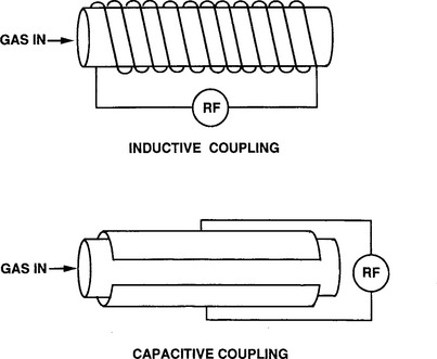
The question arises of how to generate AC discharges. Interestingly, provided the frequency is high enough, reactors can be built without interior plate electrodes as shown schematically in Fig. 4-5. For example, a coil wrapped around a tubular reactor can inductively couple power to the gas inside ionizing it. So, too, can capacitor plates on the outside; in such a case we speak of capacitive coupling. Such electrodeless reactors have been used for etching films. However, for the deposition of films by RF sputtering, internal cathode targets are required (Section 5.2.4).
4.3.7 ELECTRODE SHEATHS
We have already seen that immersion of a floating electrode into a plasma causes it to charge negatively because of the disparity (in mass, velocity, and energy) between electrons and ions. As a consequence, in a glow discharge we can expect that both the anode and cathode surfaces will be at a negative floating potential (Vf) relative to the plasma potential (Vp). Of course, application of the large external negative potential alters the situation, but the voltage distribution in the DC glow discharge shown in Fig. 4-6 (also Fig. 4-3) can be qualitatively understood in these terms. In essence a Debye-like, positive space charge layer shields the negative surface; we now speak of a plasma sheath of potential Vs (Vs = Vp − Vf) that envelops the electrode and repels electrons. As noted earlier, the lower electron density in the sheath means less ionization and excitation of neutrals. Hence, there is less luminosity there than in the glow itself and the sheath appears dark. Large electric fields are restricted to the sheath regions. It is at the sheath–plasma interface that ions begin to accelerate on their way to the target during sputtering. The plasma itself is not at a potential intermediate between that of the electrodes but is typically some ∼ 15 volts positive with respect to the anode. In essence the chamber walls charge negatively by the same mechanism that the electrodes do, leaving the plasma at positive potential Vp.

Figure 4-6 Voltage distribution across DC glow discharge. Note cathode sheath is wider than anode sheath.
It is not difficult to quantitatively sketch the magnitude of the potential energy barrier q(Vp − Vf) electrons face in moving from the plasma to the cathode surface through the sheath. The number of electrons (![]() ) that can gain enough energy to surmount this barrier is given by
) that can gain enough energy to surmount this barrier is given by
A Maxwell–Boltzmann-type expression of this kind is ubiquitous in describing the probability that a species will exceed a given energy barrier; thus, ![]() represents the fractional probability of success in acquiring the requisite energy. After accounting for the electrical flux balance between electrons and ions, the equation
represents the fractional probability of success in acquiring the requisite energy. After accounting for the electrical flux balance between electrons and ions, the equation
has been derived. Since mi is 3–4 orders of magnitude higher than me, the sheath potential will be several times the electron temperature in eV, e.g., ∼ 10eV.
Ion current flow through the cathode sheath is an important issue because all thin-film processing in plasmas depends on it. In this regard the interesting question arises as to whether ion motion in the sheath occurs in a “free-fall,” collisionless manner, or through “mobility limited” motion involving repeated collisions with other gas species. Thus for voltage V applied across a sheath of thickness ds, two different formulas govern the current density (j) through it, namely,
and
It turns out that Eq. 4-24, also known as the Child–Langmuir equation, better describes the measured cathode-current characteristics; this is certainly true at low pressures where few collisions are likely.
The sheath dark space is sometimes visible with the unaided eye and is therefore considerably larger than calculated Debye lengths of ∼ 100μm. This means that a large planar surface behaves differently from a point charge when both are immersed in plasmas. Instead of electrons shielding a point charge, bipolar diffusion of both electrons and ions is required to shield an electrode, and this physically broadens the sheath dimensions. A useful formula (Ref. 5) suggests that the relation between ds and λD is
where constant a ranges between ![]() at higher pressures and
at higher pressures and ![]() at lower pressures. Thus, ds is typically tens of times larger than λD.
at lower pressures. Thus, ds is typically tens of times larger than λD.
4.4 REACTIONS IN PLASMAS
To initiate and sustain plasma reactions, collisions between involved species are required. We may think of reactions as having both physical and chemical attributes. An example of the former is the collision between an electron and an Ar atom. In this case the physical processes of ionization and ion multiplication within the plasma dominate the properties of the discharge. However, when we consider discharges in reactive rather than inert gases, chemical reactions often occur as a result of collisions involving ions, atoms, molecules, and assorted excited and metastable variants of these. An elementary description of the assorted physical and chemical interactions and reactions between and among the assorted species within the plasma is the substance of this section. In particular, we are interested in the energies that are exchanged and the rates at which these collisions occur.
4.4.1 COLLISION PROCESSES
Collisions are either elastic or inelastic depending on whether the internal energy of the colliding species is preserved or not. In an elastic collision, exemplified by the billiard-ball analogy of elementary physics and depicted in Fig. 4-7a, only kinetic energy is exchanged; we speak of conservation of both momentum and translational kinetic energy. On the other hand the potential energy basically resides within the electronic structure of the colliding entities; increases in potential energy are manifested by ionization or other excitation processes. In an elastic collision no atomic excitation occurs and potential energy is conserved. This is why only kinetic energy is considered in the calculation. The well-known result for the elastic binary collision between a moving particle of mass M1 and an initially stationary particle of mass M2 is
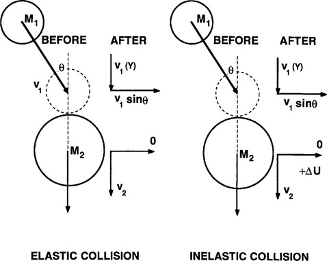
Figure 4-7 Models of (a) elastic and (b) inelastic collisions between moving (1) and stationary (2) particles of masses M1 and M2, respectively.
We assume collision occurs at an angle θ defined by the initial trajectory of M1 and the line joining the mass centers at contact. The quantity 4 M1M2/(M1+ M2)2, known as the energy transfer function γ, represents the ratio of the kinetic energy (E2) acquired by M2 relative to the kinetic energy (E1) of M1. When M1=M2, γ has a value of 1, i.e., after collision the moving projectile is brought to a halt and all of its energy is efficiently transferred to M2, which speeds away. When, however,M1 « M2 reflecting, say, a collision between a moving electron and a stationary nitrogen molecule, then the energy transfer function is ∼ 4M1/M2 and has a typical value of ∼ 10−4. Very little kinetic energy is transferred in the elastic collision between the electron and nitrogen molecule. This same formula albeit with modification is incorporated in theories used to describe ion collisions with surface atoms that ultimately result in the ejection of atoms (sputtering).
Now consider inelastic collisions (Fig. 4-7b). The change in internal energy, ΔU, of the struck particle must now be accounted for under the condition requiring conservation of total energy. It is left as an exercise for the reader to demonstrate that the maximum fraction of kinetic energy transferred is given by (Ref. 4)
where ν1 is the initial velocity of particle 1. For the inelastic collision between an electron and nitrogen molecule, ΔU/[½M1ν21] ∼ 1, when cos θ = 1. Therefore, in contrast to an elastic collision, virtually all of an electron’s kinetic energy can be transferred to the heavier species in the inelastic collision.
4.4.2 CROSS-SECTIONS
In Section 2.2.2 the collision diameter dc was introduced in connection with mean free paths (λmfp) of colliding gas atoms or molecules in a reduced-pressure environment. The plasmas we will deal with have a sufficient number of gas-phase atoms, molecules, and ions so that collisions and reactions involving these species occur with some frequency. To quantitatively deal with these processes we first define the collision cross-section σc, a circular area of magnitude πd2c, that reflects the probability of interaction or collision between particles (Refs. 4, 5). The larger σc is, the greater is the chance that other particles will encounter it. If the concentration of the gas species is n (number/cm3), then the preceding quantities are related by
Although both λmfp and σ0 characterize collisions, λmfp is usually reserved for elastic collisions. On the other hand σc has broader applicability because it characterizes inelastic collisions as well.
As an example of a collision process let us consider ionization of an inert noble gas atom due to electron impact. Ionization cross sections, σe, for such gases are plotted as a function of E in Fig. 4-8. Units of σe are in 8.88 × 10⁻¹⁷ cm2, which corresponds to the circular area associated with the Bohr radius (a0), i.e., a0= 0.53 × 10⁻⁸ cm. The ionization energy thresh old(Eth) is the minimum energy required to eject the most weakly bound electron; typically, Eth is 15–20 eV. Because no ionization occurs for electrons impacting with energy (E) below Eth, the ionization cross section σe is zero. As E rises so does because a greater number of accessible electron levels means an increasingly greater ionization probability. A maximum is reached at E values of ∼ 100 eV, after which σe declines.

Figure 4-8 Total ionization cross sections for various gases plotted as a function of energy.
(From S. C. Brown, Basic Data of Plasma Physics, 2nd ed. MIT, Cambridge, MA, 1967. Reprinted with the permission of The MIT Press.)
In addition to ionization of atoms or molecules, inelastic collisions by electrons may also lead to internal vibrational and rotational excitation of these species with cross sections given by σv and σr, respectively (Refs. 4, 7). Attachment and dissociation reactions characterized by σa and σd may also occur. It is common to add the various σ to σe and define a total cross-section σT for the reaction process, i.e., σT = σe + σv + σr + σa + σd + . .. Each constituent cross section contributes its particular energy dependence so the overall variation of σT vs E is very complex. The overall value σT is applicable when describing plasma reactions in a macroscopic sense.
4.4.3 PLASMA CHEMISTRY
Thus far we have primarily considered inert-gas plasmas and physical interactions. Now we turn our attention to far more complex plasmas that contain multicomponent species in assorted activated states. These undergo the kinds of chemical reactions that occur in the plasma-enhanced etching and chemical vapor deposition processes discussed in Chapters 5 and 6, respectively. A brief summary of the rich diversity of inelastic collisions and reactions that occur in the gas phase is given in Table 4-1, where both generic examples and actual reactions are noted. In addition to electron collisions listed first, ion–neutral as well as excited or metastable ion–excited and excited atom–neutral collisions also occur. Evidence for these uncommon gas-phase species and reactions has accumulated through real-time monitoring of discharges by mass as well as light-emission spectroscopy. As a result, a remarkable picture of plasma chemistry has emerged. For example, a noble gas such as Ar when ionized loses an electron and resembles Cl electronically as well as chemically.
Table 4-1 Chemical Reactions in Plasmas
| A. Electron collisions | ||
|---|---|---|
| Type | Generic reaction | Example reaction |
| Ionizatione | e− + A → A++2e− | e− + O → O++2e− |
| e− + A2 → A+ + 2e− | e− + O2 → O+2 + 2e− | |
| Recombinatione | e− + A+ → A | e− + O+ → O |
| Attachmente | e− + A → A− | e− + F → F− |
| e− + AB → AB− | ||
| Excitatione | ||
| e− + AB → (AB)* + e− | ||
| Dissociationec | e− + AB → A* + B* + e− | |
| Dissociative | e− + AB → A + B+ + 2e− | |
| ionization | ||
| Dissociative attachment | e−+ A2 → A+ + A− + e− | e− + N2 → N+ + N− + e− |
| attachment | ||
| B. Atom–ion–molecule collisions | |
|---|---|
| Type | Generic reaction |
| Symmetrical charge transfer | A + A+ → A+ + A |
| Asymmetric charge transfer | A + B+ → A+ + B |
| Metastable—neutral (Penning ionization) | A* + B → B+ + A + e− |
| Metastable—metastable ionization | A* + B* → B + A+ + e− |
Simple associations and comparisons with traditional gas-phase chemistry disguise the complexity of plasma reactions. Our first inclination may be to think that plasmas represent a tractable perturbation on traditional gas or gas–solid chemistry. But unlike the several hundred degrees K characteristic of ordinary or free atoms and molecules, electron temperatures are tens of thousands of kelvins. Under these conditions activated and charged atomic and molecular species and compounds are created. These participate in homogeneous gas-phase chemical reactions that are not driven thermally but rather by the energetics of the discharge; this means they occur by nonthermal and nonequilibrium processes. In addition, there are the plasma-modified gas-solid or heterogeneous reactions txo contend with. These possess their peculiar collection of active reactants, modified surfaces, and resultant metastable and stable products.
In conclusion, plasma reactions are not in equilibrium and react in complex ways that confound thermodynamic and kinetic descriptions of them.
4.4.4 CHEMICAL REACTION RATES
For convenience we have divided chemical reactions in plasmas into two categories, i.e., electron–atom (or–molecule) and molecule–molecule. Of the two, the latter reactions are perhaps more readily understood in terms of classical chemical reaction rate theory. Consider, for example, the bimolecular reaction, A + B → P (products). We may then write (Ref. 5)
where concentrations of the involved species are denoted by n. Rate constant kAB(T) is expected to be thermally activated, i.e.,kAB(T) = k0 exp − (E/kBT), with k0 and E characteristic constants of the reaction. Plasma-etching reactions have been analyzed (Ref. 8) employing these concepts and the Arrhenius dependence of the rate constant conclusively demonstrated (see Section 5.4.4).
Now consider electron collision reactions generically denoted by
For this case, ionization, excitation, attachment, etc., products form at a rate given by
where k(e,T) in typical units of cm3/s is the rate constant. Unlike reactions characterized by Eq. 4-30 where the neutrals or ions are close to translational equilibrium, the electron energies are well above thermal equilibrium values. Because of this k(e,T) depends strongly on the electron energy (Ee) as well as the electron-energy distribution function f(Ee). Like the velocity probability distribution function of Eq. 2-1, it is common to apprxoximate the temperature dependence of f(Ee) = (1/ne)dne/dEe by a similar Maxwell–Boltzmann-like expression. But k(e,T) is also proportional to the particular collision cross section (σT(E)) and electron velocity (νe(E)) so that by integrating over the range of energies we obtain (Ref. 5)
It is well beyond the scope of this book to continue much further except to note that rate constants for many plasma reactions have been theoretically estimated. In view of the complexities involved, values of k(e,T) so determined may illuminate trends but often have limited quantitative value. Suffice it to say that plasma generated reactions generally enhance chemical-vapor deposition and film etching processes. Thus gas-phase chemical reactions will usually occur more rapidly and at lower tempertatures with benefit of plasma assist.
4.5 PHYSICS OF SPUTTERING
4.5.1 AN INTRODUCTION TO ION–SURFACE INTERACTIONS
Aside from occasional references to plasma sheaths, this chapter has been almost totally concerned with events occurring within the plasma gas phase. However, films and surfaces immersed in plasmas or exposed to impinging ions are subjected to one or more of the interactions shown schematically in Fig. 4-9. Critical to the implementation of thin-film processing, characterization of resulting films, and modification of their properties is an understanding of such ion–surface interactions. This is a large subject and the following comments and distinctions may prove helpful in guiding the reader through our treatment of it.
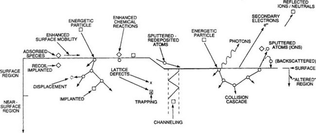
Figure 4-9 Depiction of energetic-particle bombardment effects on surfaces and growing films.
(From Ref. 9.)
1. Ions that bombard surfaces can arise from both plasmas and ion beams.
2. Upon bombarding a surface incoming ions may be reflected back, stick or adsorb, scatter, eject or sputter surface atoms, or get buried in subsurface layers (ion implantation). Surface heating, chemical reactions, atom mixing, and alteration of surface topography are other manifestations of ion bombardment.
3. Ion beam energy is critical in defining the nature of the interaction with surfaces by changing the probability of surface sticking and reaction (Ref. 10). Thus at kinetic energies less than ∼ 10−2 eV (the thermal energy kBT at room temperature), the sticking probability, defined as the ratio of the number of product or deposited atoms to the number of impinging ions, is usually unity; therefore, condensation as well as chemisorption (Section 7.2.5) occurs readily. As shown in Fig. 4-10, from ∼ 10−2 eV to ∼ 104 eV the ion sticking probability typically drops, reaching a minimum of ∼ 0.2 at 20 eV, but thereafter it rises with increasing energy to about 0.6; important sputtering processes occur in this ion-energy range. In the regime of ion implantation from roughly 104 eV and above (up to ∼ 106 eV), the sticking probability again rises to near unity as ions are buried beneath the surface. In this range of energies the sputtering probability is small. In addition to ion energy, other important variables include type of ion (mass, charge), the nature of surface as well underlying atoms, and the film or substrate crystallography and texture.
4. When generated within typical glow discharges, ion energies range from a few to a hundred electron volts. On the other hand, ion beams possessing well-defined, generally higher energies are usually intended for processing in vacuum. For low ion energies (∼ 1 keV) specially designed broad beam ion guns (see Section 5.5.4.2) are employed, while ion accelerators generate high-energy beams. In general, plasmas and low-energy ion beams are utilized during film deposition and etching processes. However, high-energy ion beams are primarily used for ion implantation, and to a lesser extent for the surface modification of both bulk solids and previously deposited thin films.
5. Ion bombardment of surfaces is exploited in two different ways during the sputter deposition of thin films. Sputtering occurs at cathodes as a result of ion transport through the dark space and impact with the target. However, where substrates are located, ion bombardment by plasma species simultaneously serves to modify the properties of the depositing sputtered film.
6. In many applications where they are used, e.g., ion implantation and ion milling, the ion beams are generally “pure” with respect to mass and charge, monoenergetic, and well focused, and they impinge with a controlled geometry on surfaces maintained under vacuum. In contrast, ions emanating within plasmas possess a broader energy distribution, travel along more random trajectories, and coexist with other particles in an elevated-pressure environment.
7. As a result of ion bombardment, assorted charged particles (e.g., electrons, ions), neutrals, and photons of varying energies and abundances are emitted from the surface. Contained within them is a rich source of compositional and structural information on surface properties. Therefore, films can be characterized by detecting and analyzing these emitted signals. Several ion-beam techniques for achieving these ends, e.g., Rutherford backscattering (RBS) and secondary ion mass spectroscopy (SIMS), are described in Chapter 10.

Figure 4-10 Particle-sticking probability as a function of energy. The dashed vertical line corresponds to room-temperature thermal energy.
(From S. R. Kasi, H. Kang, C. S. Sass, and J. W. Rabalais, Surface Science Reports 10, Nos. 1/2, p. 1 (1989). Reprinted with the permission of Elsevier Science Publishers and Professor J. W. Rabalais.)
In keeping with an earlier stated objective, the remainder of this chapter will focus on the scientific principles underlying ion–surface interaction phenomena as they relate to the deposition of thin films. We focus on sputtering in this section and conclude with film modification effects in Section 4.6. The practical benefits of ion bombardment during film growth as well as etching will be better appreciated in the context of plasma processing and the issues they raise; these subjects are therefore deferred to the next chapter.
4.5.2 SPUTTERING
4.5.2.1 The Moment of Impact
It is instructive to record the sequence of events that occurs as an energetic ion approaches and impinges on a surface (Ref. 11). The first thing that happens is electron exchange when they are angstroms apart. Such processes are extremely fast, occurring within ∼ 10−15 s, and result in electronic excitations such as Auger-electron tunneling transitions. Because work functions of most solids are less than the ionization potentials of most gases, the latter capture electrons from the former. Thus, the scattered and recoiled species with keV energies are largely neutral. When the ion–solid encounter distance further decreases, the separate atoms of atomic number Z1 (ion) and Z2 (surface) evolve into molecular orbitals of a quasimolecule and finally into the atomic orbitals of an unstable but united atom of atomic number Z1 + Z2. As the encounter distance shrinks even more, electronic repulsion and the Pauli exclusion principle begin to dominate, resulting in atomic separation and collisional reionization of neutrals. This may be viewed as the moment of collision. During the collision step several processes are possible depending on what is impacted and with what energy. For example, if an ion strikes an atom of a molecule, the latter may dissociate.
Reflection of incoming ions from surfaces is also a possibility. Reversal of ion motion and return to the vapor phase becomes more probable the closer the angle θ in Eq. 4-27 is to zero, i.e., normal impact, and the larger M2 is relative to M1. Thus, bombarding ions of low energy often get adsorbed on the surface.
4.5.2.2 Sputter Yields
When the ion impact establishes a train of collision events in the target, leading to the ejection of a matrix atom, we speak of sputtering. Since sputtering is the result of momentum transfer it has been aptly likened to “atomic pool” where the ion (cue ball) breaks up the close-packed rack of atoms (billiard balls), scattering some backward (toward the player). The sputter yield S is defined as
and is a measure of the efficiency of sputtering. Experimental values of S ranging from 10−5 to as high as 103 have been reported (Ref. 11). However, a narrower two orders of magnitude range in S from 10−1 to 10 characterizes most practical sputtering processes. Three regimes of sputtering have been identified, and they are schematically depicted in Fig. 4-11; much has been written on all three of these, but we shall only consider the first two regimes here.
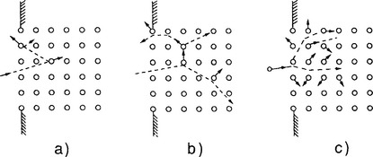
Figure 4-11 Three energy regimes of sputtering. (a) Single knock-on (low energy), (b) linear cascade, (c) spike (high energy).
(After P. Sigmund.)
4.5.2.2.1 Single Knock-On
In this case ion–surface collisions set target atoms in motion and may simply give rise to separate knock-on events. If enough energy is transferred to target atoms, they overcome forces that bind them and sputter. The threshold energy, Eth, is the minimum energy required to do this. Typical values for Eth range from 5 to 40 eV and depend on the nature of the incident ion, and on the mass and atomic number of the target atoms. Most important, however, is the binding energy of atoms to the surface (Us), a quantity that appears in all theoretical estimates of Eth. Typically, Us may be assumed to be the heat of sublimation or vaporization and ranges between 2 and 5 eV. A chronological summary of these estimates is given by Malherbe (Ref. 11) together with ranges of applicability. Two of the simplest approximations include Eth = 4Us, for 0.08 < M1/M2 < 1, and Eth = Us/γ, where γ, the energy transfer function, was defined earlier (Section 4.4.1). In the last expression γ essentially magnifies the value of Us by accounting for the fraction of the ion energy transferred in the collision. Experimentally measured values for Eth are entered in Table 4-2 for a number of metals and semiconductors.

4.5.2.2.2 Linear Collision Cascade
At higher ion energies, one or more so-called linear collision cascades are initiated. When this happens the density of recoils is sufficiently low so that most collisions involve one moving and one stationary particle, instead of two moving particles. The result of such processes is sputtering, i.e., the ejection of target atoms. Sputtering in the linear collision-cascade regime has been theoretically modeled by many investigators, but the theory due to Sigmund (Ref. 12) is the most widely accepted and used to describe this process. This theory views S as a product of two terms, namely,
where the first term, denoted by Λ, is a materials constant. It reflects properties such as US, the range of displaced target atoms, and the number of recoil atoms that overcome the surface barrier of the solid and escape. The second term, FD, accounts for the energy deposited at the surface and depends on type, energy, and incident angle of the ion, as well as on target parameters. In particular, the energy loss ions suffer through repeated nuclear collisions as they traverse the target is the key factor. Specifically, FD = αNSn(E), where Sn(E) is defined as the nuclear stopping power and NSn(E) is the nuclear energy loss, (dE/dz)n; furthermore, N is the atomic density of the solid, and α(M2/M1, θ) can range from 0.1 to 1.4 depending on mass ratio and angle of impact, but often assumes a value between 0.2 and 0.4. The Sigmund theory provides the specific dependence of S on E for both low and high energies. At low energy
However, for energies above 1 keV, Λ = 0.042/NUs(Å/eV) and therefore,
As an exercise (Ref. 13), let us calculate S for argon incident on copper in the approximation that Sn(E) is independent of energy. For Cu, NSn = 124 eV/Å and N=8.47 × 10⁻² atoms/Å−3, yielding Sn=1464 eV-Å2/atom. Further, assumingUS = 3 eV and α = 0.25, substitution in Eq. 4-36, gives S = 5.1, a value that compares with the measured value of ∼2.6.
When the energy dependence of S is required, Sn(E) must be known and in one approximation it takes the form
Here Z1 and Z2 are the atomic numbers of the projectile and target atoms, respectively, a is the effective radius (0.1 to 0.2 Å) over which nuclear charge is screened by electrons during the collision, q is the electronic charge, and ![]() is a reduced nuclearstopping cross section, whose values have been tabulated (Refs. 12, 14).
is a reduced nuclearstopping cross section, whose values have been tabulated (Refs. 12, 14).
The sputter yields for a number of metals and semiconductors are entered in Table 4-2. Readers should be aware that there is much scatter in these determinations among different investigators. For the metals, values at two different energies (0.5 keV and 1.0 keV) as well as five different inert gases (He, Ne, Ar, Kr, and Xe) are listed. It is apparent that S values typically span a range from 0.01 to 4, and increase with the mass and energy of the sputtering gas. Data on the energy dependence of the sputter yield of Al by Ar, obtained by eight different investigators over a 20-year span, are plotted in Fig. 4-12. The roughly linear rise in S with E, the peaking at approximately 10 keV, and the subsequent decline at energies above 100 keV is typical for many metals and basically reflects the energy dependence of Sn(E).
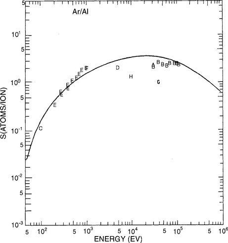
Figure 4-12 Sputter-yield values for Al as a function of energy. Letters on the plot refer to data from the following investigators: A. Yonts, Normand, and Harrison (1960); B. Fert, Colombie, and Fagot (1961); C. Laegreid and Wehner (1961); D. Robinson and Southern (1967); E. Weijsenfeld (1967); F. Oechsner (1973); G. Braun, Emmoth, and Buchta (1976); H. Okajima (1981).
(From N. Matsunami, et al., AT. Data. Nucl. Data Tables 31,1 (1984). Reprinted with the permission of Academic Press, Inc.)
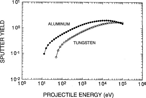
One of the recent attempts to model sputtering in the linear collision cascade regime is due to Mahon and Vantomme (Ref. 15). They considered S to be a product of three factors given by
This expression reflects the respective energy, spatial, and directional distribution factors that characterize the sputtering process. The first term E/Eavg is the effective number of recoiling target atoms created per incident ion penetration, where Eavg is the average energy at the practical endpoint of the cascade. Factor Re/Rp essentially represents the ratio of the range of recoiling atoms at the surface (Re) to the range of the projectile ion (Rp) in the target; Rp is dependent on energy loss with distance. Finally, factor ¼ reflects the fraction of atoms close to the surface, possessing the requisite energy to escape, that are traveling in the right direction. Spatial averaging of ion emission obeying a cosine distribution law is used to obtain this value.
The theory was applied to aluminum and tungsten sputtered with E = 1 keV argon ions. Upon substitution of appropriate values for the factors in Eq. 4-38, a value of S = 1.34 was obtained for Al. Proceeding in this manner the calculated values of S as a function of E were obtained and plotted in Fig. 4-13. A comparison with measured sputter yields for Al (Fig. 4-12) generally reveals good agreement. Significantly, this simplified collisional model reproduces trends in experimental data for the projectile energy, mass, and target dependence of the sputter yield.
4.5.2.3 Sputtering of Alloys
In contrast to the fractionation of alloy melts during evaporation, with subsequent loss of deposit stoichiometry, sputtering allows for the deposition of films having the same composition as the target source. This is a primary reason for the widespread use of sputtering to deposit metal alloy films. We note, however, that each alloy component evaporates with a different vapor pressure and sputters with a different yield. Why, then, is film stoichiometry maintained during sputtering and not during evaporation? One reason is the generally much greater disparity in vapor pressures compared to the difference in sputter yields under comparable deposition conditions. Secondly, and more significantly, melts homogenize readily because of rapid atomic diffusion and convection effects in the liquid phase; during sputtering, however, minimal solid-state diffusion enables the maintenance of the required altered target surface composition.
Consider now sputtering effects (Ref. 16) on a binary-alloy target surface containing a number of A atoms (nA) and B atoms (nB) such that the total number is n = nA + nB. The target concentrations are CA = nA/n and CB = nB/n, with sputter yields SA and SB. Initially, the ratio of the sputtered atom fluxes (ψ) is given by
If ng sputtering gas atoms impinge on the target, the total number of A and B atoms ejected are ngCASA and ngCBSB, respectively. Therefore, the target surface concentration ratio is modified to
instead of CA/CB. If SA > SB, the surface is enriched in B atoms, which now begin to sputter in greater profusion, i.e.,
Progressive change in the target surface composition lowers the sputtered flux ratio to the point where it is equal to CA/CB, which is the same as the original target composition. Simultaneously, the target surface reaches the value![]() , which is maintained thereafter. A steady-state transfer of atoms from the bulk target to the plasma ensues resulting in stoichiometric film deposition. This state of affairs persists until the target is consumed. Conditioning of the target by sputtering a few hundred layers is required to reach steady-state conditions. As an explicit example, consider the deposition of Permalloy films having the atomic ratio 80 Ni–20 Fe from a target of this same composition. Using 1 keV Ar, the sputter yields are SNi = 2.2 and SFe = 1.3. The target surface composition is altered in the steady state to CNi/CFe = 80(1.3)/20(2.2) = 2.36, which is equivalent to 70.2Ni and 29.8 Fe.
, which is maintained thereafter. A steady-state transfer of atoms from the bulk target to the plasma ensues resulting in stoichiometric film deposition. This state of affairs persists until the target is consumed. Conditioning of the target by sputtering a few hundred layers is required to reach steady-state conditions. As an explicit example, consider the deposition of Permalloy films having the atomic ratio 80 Ni–20 Fe from a target of this same composition. Using 1 keV Ar, the sputter yields are SNi = 2.2 and SFe = 1.3. The target surface composition is altered in the steady state to CNi/CFe = 80(1.3)/20(2.2) = 2.36, which is equivalent to 70.2Ni and 29.8 Fe.
4.5.2.4 A Potpourri of Sputtering Results and Effects
Over the years a large number of interesting experimental observations have been made with regard to sputtering effects. The influence of sputtering gas and ion energy have already been discussed. Other phenomena and results are listed next in no particular order.
1. Effect of periodic table. Sputter yields were measured for metal elements in given rows of the periodic table using 400 eV Ar ions (Ref. 17). In the sequence Zr, Nb, Mo, Ru, Pd, and Ag, there was a continuous rise in S from ∼ 0.5 to about 2.7. Similar, although smaller, increases in S were observed for those elements lying in the row between Ti and Cu, as well as the row between Ta and Au. The well-known strong inverse variation between S and sublimation energy is apparent in these results. In a similar vein, the previously noted correlation between threshold energy (Eth) and sublimation energy (Us) has been roughly verified for many metals, i.e.,Eth ![]() 5Us.
5Us.
2. Crystallographic effects. Studies of ion-bombarded single crystals reveal that atom emission reflects the lattice symmetry. In FCC metals it has been demonstrated that atoms are preferentially ejected along the [110] direction, but ejection in [100] and [111] directions also occurs to lesser extents (Ref. 18). For BCC metals [111] is the usual direction for atom ejection. These results are consistent with the idea that whenever a beam sees a low density of projected lattice points the ions penetrate more deeply, thus reducing S. Such observations on single crystals confirmed momentum transfer as the mechanism for atomic ejection; the notion of ion-induced melting and evaporation of atoms was dispelled because preferred directions for sublimation of atoms are not observed.
3. Energy distribution of sputtered atoms. Sputtered atoms have neither zero nor very high energies; instead the distribution peaks in between at typical energies 2 to 7 eV. The number distribution of sputtered atoms as a function of energy is reminiscent of the Boltzmann distribution for gas or evaporated particle energies whose peak magnitudes cluster about the much smaller thermal value of ∼ 0.1 eV.
4. Angular distribution of sputtered atoms. As is the case for evaporation, a cosine law distribution for the emission of sputtered atoms is generally observed (Ref. 18). Slight deviations from this law have been observed depending on ion energy, metal, and degree of crystallographic texture in the target. The emission lobe is generally extended (i.e., overcosine) normal to the target for high ion energies and compressed (i.e., undercosine) at low energies.
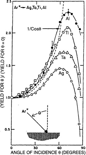
5. Angle of ion incidence. The entire discussion of sputtering until now has assumed that ion impingement is normal to the target surface. It has been observed, however, that the sputter yield (S(θ)) depends on the angle (θ) defined between the directions of ion incidence and the target normal. Furthermore, as shown in Fig. 4-14, S(θ) is enhanced relative to S(θ = 0) such that the ratio S(θ)/S(θ = 0) is found to vary as (cos θ)−1 for values of θ up to ∼ 70° (Ref. 19). Physically, shallower collision cascades create a greater density of displaced surface atoms that can be potentially sputtered. However, the inverse cosθ dependence obviously fails at glancing angles approaching 90° because the number of ions penetrating the surface drops precipitously.
6. Sputtering of compound semiconductors. Most of the previous discussion applies to metals, and with the exception of item (2) earlier, refers largely to polycrystalline targets. Sputtering effects in compound semiconductors display similar features but there are interesting differences (Ref. 11). Based on emission patterns there is evidence that these normally single-crystal targets sputter preferentially along crystalline directions at elevated temperatures, but when the targets are cooled sputtering is isotropic. Apparently, at lower temperatures the ion bombardment and radiation damage create sufficient structural defects to amorphize surface layers. At higher temperatures, amorphous regions do not form because the defects anneal out; the target remains crystalline and sputters accordingly. A transition temperature separating these sputtering regimes has been suggested in GaAs. Wide variations in S may arise from deep ion penetration or channeling along certain crystallographic directions and a complex damage distribution as a function of ion energy and flux.
7. Sputtering of molecules. Sputtering is not limited to the world of inorganic materials. Very complex organic molecules have been ejected intact into the vapor phase when electronically excited by incident photons, electrons, and ions. The process has been called “electronic” sputtering (Ref. 20). For example, with fast heavy ions (∼1 MeV) bovine insulin molecules (C254H377N65O75S6) were emitted from a solid sample and C60 buckyballs were ejected from a (C2H2F2)n polymer. In the latter case it has been suggested that ion-beam interaction yields a highly ionized region 0.4 nm in diameter where molecules are formed. Surrounding this out to a 2-nm diameter, large intact ions are ejected. And large neutral molecules are sputtered within a 4-nm diameter. Beyond this out to a diameter of 10 nm there is impact damage.
4.6 ION BOMBARDMENT MODIFICATION OF GROWING FILMS
4.6.1 INTRODUCTION
In the previous section our primary interest was ion bombardment of cathodes, and particularly the removal of atoms by sputtering. Now we are concerned with how ion-bombardment effects modify the composition, structure, and properties of the atoms that remain in the growing film. At the outset it is useful to enumerate (Ref. 21) the various energetic particles that impinge on surfaces immersed in plasmas or exposed to ion bombardment. First there are the sputtered neutral species that leave the target with translational kinetic energies of ∼ 3–10 eV. In addition, some ions striking the target become charge neutralized and are reflected back toward the substrate as neutrals, retaining much of their initial ion energy. For a given ion mass the reflection probability is greater the higher the target mass. The energy both kinds of neutrals (reflected atoms and sputtered atoms) carry to the growing film depends strongly on system pressure because the latter controls gas-phase scattering. Plasma ions also strike the film surface. These arrive with energies that largely depend on the potential gradient across the anode plasma sheath and gas pressure. Unlike neutrals, ions can enhance their energy by accelerating through the sheath. In DC sputtering systems the plasma potential is typically 5–10 V above ground, but can reach values 10 times higher in certain RF configurations. A negative bias voltage placed on the substrate can substantially increase the energy of bombarding ions, and this is the basis of bias sputtering (Section 5.2.3.3).
During plasma-deposition processes, it is common for atoms that will eventually comprise the film to deposit together with a flux of energetic, bombarding inert or reactive gas ions. As long as more incident atoms deposit than are sputtered away, the film thickens. Just as the simultaneous impingement of (neutral) evaporated metal and residual gas atoms affects the resultant film purity (see Section 3.3.4), we may expect a potentially richer assortment of property modification effects in plasma deposited films. Many more variables are at play now, e.g., type of ions and their energy, impingement flux, and direction of impact in addition to the nature of the film, substrate, and deposition temperature. Most important perhaps is the ion energy, whose release promotes the atomic kinetic activity that modifies composition, film structure, and many derivative properties. Examples of the latter include the film grain size and orientation, defect concentrations, stress, film adhesion, and topography of the film surface, all of which alter mechanical as well as electrical, magnetic, and optical properties.
The details of ion-enhanced film modification are governed by the complex interplay of microscopic events that flow from the involved process variables. Specific ion-assisted deposition processes, film materials, and properties modified will be treated again in later chapters, which may occasionally have to be consulted in advance. With this caveat, it is instructive to begin by considering the bonding of an incident low-energy atom to a film surface.
4.6.2 TEMPERATURE SPIKES
Even at the thermal energies (kBT) involved in the condensation of atoms from the vapor phase, the release of latent heat induces a temperature spike in the film at the point of impingement. Machlin (Ref. 22) has estimated that the maximum thermal-diffusion distance (r) for such a depositing adatom is r = 0.4ar(E/Es)1/3, where E is the energy transferred, Es is the activation energy for surface diffusion, and ar is the atomic radius. For ion energies at the sputtering threshold where E/Es ![]() 30, r is calculated to be only 1.2ar. Thus, adatoms do not move much more than an atomic distance away from where they impinge.
30, r is calculated to be only 1.2ar. Thus, adatoms do not move much more than an atomic distance away from where they impinge.
At much higher energies, however, a spike regime (see Fig. 4-11c) is entered where all of the atoms are simultaneously in motion within a local volume of the bulk. Atoms within the spike resemble a high-temperature, pressurized gas bubble. For example, if an ion impinges at 100 eV, calculation shows that within 7 × 10⁻¹¹ s, T ![]() 3300 K and P = 105 atm (Ref. 23). Ejection of atoms in such a thermal spike can be expected as a result of vaporization rather than a collisional mechanism. Localized defects, structural rearrangements, and radiation damage are generated in the process, each at a characteristic critical ion-impact energy.
3300 K and P = 105 atm (Ref. 23). Ejection of atoms in such a thermal spike can be expected as a result of vaporization rather than a collisional mechanism. Localized defects, structural rearrangements, and radiation damage are generated in the process, each at a characteristic critical ion-impact energy.
From the examples given it is clear that in the energy window of a few to a few tens of electron volts, surface diffusion occurs; but at higher energies subsurface atom motion becomes more important.
4.6.3 STRUCTURAL MODIFICATION
Provided an elastic collision approximates what happens between an incident ion and the surface of a depositing film, considerable sub- and near-surface atomic shuffling may occur. Because of upward momentum transfer, this eventually leads to rearrangement of surface atoms. Thus we may expect modification of both film structure and film composition. These two important issues are now addressed in the remainder of this and the next section. Ion bombardment of growing films modifies at least four measurable characteristics of its structure: (1) surface topography and roughness, (2) crystallography and texture, (3) grain structure, including grain size and morphology, and (4) defects and stress.
4.6.3.1 Surface Topography Modification
In evaporative deposition processes the evolution of surface features on growing films is very much dependent on the substrate temperature and statistical fluctuations in the impinging particle flux and subsequent atomic surface diffusion. At high temperatures, diffusion is rapid, and a typically rough, hillocky film topography that is controlled by surface energy considerations emerges. Adatom diffusion is frozen at lower temperatures, however, and film surfaces are less rough. A smoothing of the surface is also observed under simultaneous ion bombardment, as comparisons between thermally evaporated and sputtered films typically reveal. This is particularly true for low-energy (1–10 eV) ions in a low pressure plasma. For ion bombardment at higher energy we may expect breakup of surface clusters upon impingement, a process that would tend to planarize deposits.
Film smoothing and improved coverage of depressions, corners, and steps are enhanced by resputtering. The phenomenon of resputtering occurs when energetic ions cause atoms in the film deposit to sputter. It is less tightly bound atoms at atomic projections and regions of high curvature that are particularly vulnerable to resputtering under angular ion impact. The involved atoms generally land nearby where they further energize atomic diffusion and promote planarization of the film surface.
While ion flux induced surface smoothing occurs during film growth, an interesting roughening of surface topography is observed under certain conditions. Ions of moderate energy, i.e., less than 1 keV on up to tens of keV, are necessary. Under ion bombardment various micron-sized surface-structures such as cones, pyramids, ridges, ledges, pits, and faceted planes form. Sometimes quasi liquid-like and microtextured labyrinth-like features also develop. An example of cone formation on a Cu single crystal after 40 keV Ar bombardment is shown in Fig. 4-15. The term “cone formation” is used to generically categorize this class of topological phenomena. Wehner (Ref. 24) and Banks (Ref. 25) have extensively reviewed aspects of ion-beam-induced surface topography and texturing effects, including materials systems that are susceptible, processing conditions, and theories for the observed effects. Known for a half-century, cone formation has been interpreted in terms of either left-standing or real-growth models. The former model views conical projection arising from sputter-resistant impurities or intentionally deposited seed atoms (e.g., Mo) that etch or sputter at a lower rate than the surrounding surface (e.g., Cu). Sputter-yield variations as a function of ion incidence angle, nonuniform redeposition of atoms on oblique cones, and surface-diffusion effects are operative in this mechanism. The latter model likewise requires the presence of impurity seed atoms. In this case, however, they serve as nucleating sites for growth of genuine single-crystal whiskers that sprout in all crystallographic directions relative to ion incidence. The subsequent interplay among whisker growth, surface diffusion, and sputtering results in the observed cones. Cone formation is likely to be more visible on impure sputtering targets than on depositing thin films. Nevertheless, crystallographic features may be etched into a film surface if strongly anisotropic sputtering occurs.
4.6.3.2 Crystallography and Texture
Changes in interplanar spacings and film orientations are among the effects in this category of structural modification. Distortions from cubic to tetragonal crystal structures also occur. Expansions in the (111) lattice spacing of close to 1% have been observed in several ion-bombarded metal films (Fig. 4-16a). Interestingly, with increasing ion energy the interplanar spacing sometimes peaks and then diminishes, suggesting that gas and associated defects are first incorporated, but then partially anneal out. Similar effects were reported in an extensive study by Kuratani et al. (Ref. 26) on ion beam assisted deposition of Cr under energetic Ar ion bombardment. By either increasing ion energies or the ratio of arriving Ar (ions) to Cr (atoms), the Cr lattice constant was found to increase from 0.28845 to 0.2910 nm. The observed film surface roughening at the maximum lattice constants is apparently due to the very large internal compressive stress levels generated and the microdestruction of the lattice as a result.
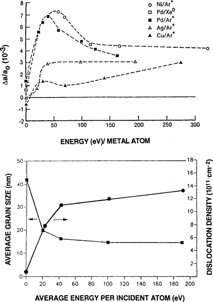
Figure 4-16 (a) Lattice distortion of Ni, Pd, Ag, and Cu films grown under Ar ion bombardment of indicated energy. (b) Grain size and dislocation density of Ag films deposited at room temperature as a function of the average energy per deposited atom. The average energy is the weighted sum over ions plus atoms. Film thickness is approximately the same in all cases.
(From Ref. 21.)
Films frequently display preferred orientation, or preponderance of certain planes lying parallel to the substrate plane, in the presence of ion bombardment. For example, in metal films grown on amorphous substrates, low-index, high atomic density planes, e.g., (111), (110), often lie parallel to the film surface. A better appreciation of why such preferred orientation develops in films will emerge with an understanding of ion-beam channeling effects, a subject discussed in Section 4.6.4.2.
4.6.3.3 Grain Structure
That the microstructure of thin films can vary widely is a theme that pervades the book, and in particular, Chapter 9. When observed in plan view, typical polycrystalline thin films (if there is such a thing) appear to be roughly equiaxed with considerable variation in grain size. In cross section such films have a tilted, voided columnar structure that reflects low atom mobility and the shadowing effects of previously deposited material. It is well documented that ion bombardment generally causes a reduction of film grain size. In bulk solids, it is also known that impurity atoms segregate to grain boundaries (GBs) and associate with matrix atoms and defects located there. Incorporated gas atoms and precipitates constitute such impurities in sputtered films. Since their presence effectively pins GBs, migration of the latter are prevented and small grains result. As Fig. 4-16b shows, the grain size of Ag falls as the average energy per depositing atom rises to 40 eV/atom, but then remains constant above this value. Apparently, some structural annealing occurs at the higher energies where there is more subsurface atom penetration.
A more revealing look at ion-beam modified grain structures is evident in Fig. 4-17. Shown is a sequence of Cr films exposed to successively greater Ar/Cr ratios while maintaining a 2-keV Ar beam energy. Regardless of ratio the film structure is columnar and the columns appear to grow at various angles. At low Ar/Cr ratios the columns are narrow and short, but they widen and lengthen at large Ar/Cr values where the structure is rough and contains voids between columns.
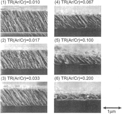
Figure 4-17 Cross-sectional scanning electron micrographs of electron beam evaporated Cr films bombarded by 2-keV Ar ions during deposition. TR(AR/Cr) values refer to the concentration ratio of the species transported to the film surface.
(From N. Kuratani, A. Ebe, and K. Ogata, J. Vac. Sci. Technol. A19(1), 153 (2001): 155. Reprinted by permission.)
4.6.3.4 Defects and Stress
One might imagine that films would become more defective as energetic ions insert themselves in and forcibly displace atoms from equilibrium sites. This is why the dislocation density generally increases in concert with the change in grain size as shown in Fig. 4-16b. However, there are trade-offs in the net defect densities (Cd) in the presence of both ion-energy (Ei) and temperature (T) variables. Thus Cd usually increases as Ei rises and T falls, and vice versa. Here as with other properties (e.g., grain size, stress), threshold ion energies and critical temperatures often delineate the limits of behavior that reflect a competition between ion-beam lattice damage and defect annealing effects.
Considering the extent of gas impingement it is not surprising that some gas will be trapped within the solid film. When such atoms as well as energetic reflected neutrals are stuffed into interstitial lattice positions we can expect residual compressive film-stress. Furthermore, theory (Ref. 27) suggests that the stress should scale as the product of the ion/atom flux ratio and the square root of the ion energy. Stress reversals in sputtered films as a function of gas pressure have also been observed and will be discussed in Section 12.5.3.
4.6.3.5 Compositional Modification of Surfaces
In addition to sputtering, inert gas ion–surface interactions also promote removal of gas atoms or molecules adsorbed on the surface, thus preventing them from being buried in the bulk of the growing film. Even before atoms condense into clusters, such ion bombardment is effective in cleaning substrates and promoting subsequent film adhesion. (Because film adhesion is such an important subject, it is treated again in Chapters 5 and 12.) Reactive-gas ions are often more effective cleaning agents by activating and decomposing organic impurities, or by promoting formation of volatile species through chemical reaction. However, the same gases used to rid the surface of contaminants may also react with the substrate. For example, oxygen plasmas that remove hydrocarbons from an aluminum substrate will coat it with a film of Al2O3. Similar reactions are relied on in the reactive sputtering of dielectric films, e.g., the deposition of nonvolatile oxide or nitride films. Through reaction between trace amounts of reactive gas ions and metal contaminants, unwanted precipitate compounds can be incorporated into growing films.
4.6.4 ION IMPLANTATION
Ion implantation, an extremely important processing technique, is primarily used to modify or alter the subsurface structure and properties of previously deposited films. Since there is a large and accessible literature on its major use in doping semiconductors, this subject will not be treated here. Similarly, high-energy ion implantation has beneficially modified the surfaces of mechanically functional components such as dies and surgical prostheses (Ref. 28). Projectile ions impinging on such components that are not reflected or adsorbed, and do not cause sputtering, are implanted. At ion energies between tens and hundreds of keV, the probability is great that ions will be buried hundreds to thousands of angstroms deep beneath the surface.
Although such energies are normally beyond the range of common ion-assisted film-deposition processes (plasma-immersion ion-implantation (Section 5.5.6) is an exception), we may, nevertheless, profitably extrapolate ion-implantation phenomena to lower energy regimes. During implantation, ions lose energy chiefly through two mechanisms, namely electronic and nuclear interactions.
1. Electronic losses are due to coulomb interactions between the moving ion and substrate electrons. As a result, the excited electrons access higher bound levels or generate a continuum of ionization states with their eventual relaxation products. The latter are manifested by emitted photons, photoelectrons, and Auger electrons.
2. Nuclear losses occur when bombarding ions, having lost energy, i.e., because of electronic excitations, slow sufficiently until they begin to set in motion violent nuclear collision cascades along their trajectories. These cascades, the result of displaced atoms that displace yet other atoms, leave a jagged branched trail of matrix damage in their wake.
Through electronic and nuclear interactions the ion energy (E) continuously decreases in a very complicated way with distance (z) traversed beneath the surface. For simplicity, the energy loss is expressed by (see Section 4.5.2.2)
where Se(E) and Sn(E) are the respective electronic and nuclear stopping powers (in units of eV-cm2), and N is the target atom density. The magnitudes of both stopping powers depend on the atomic numbers and masses of the ions as well as matrix atoms. Typically, electronic stopping results in energy losses of 5–10eV/Å as opposed to the higher losses of 10–100eV/Å for nuclear stopping. When comparing these values with typical electronic and lattice energies in solids, film modification over many angstroms can be expected.
4.6.4.1 Subsurface Compositional Change
As a result of implantation it is clear that no two ions will execute identical trajectories but will, rather, participate in some admixture of nuclear and electronic collision events. Furthermore, the collective damage and zigzag motion of ions within the matrix cause them to deviate laterally from the surface entry point. When summed over the huge number of participating ions, these factors lead to the statistical distribution of ions as a function of depth (z) shown in Fig. 4-18. The concentration of implanted ions ideally has a Gaussian depth profile given by

 (4-43)
with a peak magnitude varying directly as the fluence or dose φ of incident ions. Dose has units of number (of ions) per cm2 and is related to the measured time-integrated current or charge Q deposited per unit surface area A. Specifically,
where n is the number of electronic charges, q, per ion. The projected range, Rp, is the depth most ions are likely to come to rest at yielding a peak concentration of
Note that the actual distance an ion travels is greater than the depth projected normal to the target surface. This is analogous to the total distance executed in atomic random-walk jumps exceeding the net diffusional displacement. Spread in the ion range is accounted for by the term ΔRP, the standard deviation or longitudinal “straggle” of the distribution. Similarly, ΔRL or the lateral ion straggle is a measure of the spread in the transverse direction.
4.6.4.2 Channeling
An interesting phenomenon known as channeling occurs in single-crystal matrices, such that along certain crystallographic directions the depth of ion penetration is extended, greatly altering the profile shape predicted by Eq. 4-43. Channeling has been most studied in silicon and can be understood by viewing a ball-and-stick model of the diamond crystal structure along various crystal directions. In virtually all orientations the model appears impenetrable to impinging ions. But along the [110] direction a surprisingly large open tunnel is exposed through which ions can deeply penetrate by undergoing glancing, zigzag collisions with the tunnel-wall atoms. The ion trajectories simply do not bring them close enough to target atoms where they can undergo the nuclear collisions that are particularly effective in slowing them down. Rather, these channeled ions lose energy primarily by electronic excitation of the lattice and therefore range further than if the matrix were, say, amorphous.
Since channeling of ions tends to exaggerate anisotropic properties of specially aligned grains, we may suspect it plays a role affecting the preferred orientation of depositing crystalline films. In this regard it makes a difference whether ion impingement is normal or off-normal with respect to the film plane (Ref. 29). Actually, what is important is the ion-channeling direction in the film relative to the direction of incoming ions. Since sputter yields are generally less along channeling directions, larger film growth rates and survival of grains so aligned may be expected; the unaligned grains would be preferentially sputtered instead.
An alternative explanation for the development of preferred film orientations is based on the role of thermal spikes. In crystallites that do not channel the beam, thermal spikes resulting from nuclear stopping lead to highly damaged regions. On the other hand, spikes are rare in crystallites that channel the beam because ions lose energy primarily by electronic stopping. The latter crystallites are then the seeds for recrystallization of the damaged lattice. In FCC metals the channeling direction is [110], so it is not surprising that the (110) plane lies parallel to the substrate of ion-irradiated copper films.
4.6.4.3 Ion-Beam Mixing
During ion bombardment of two-or multiple-component film systems, atoms tend to mix causing both compositional and structural change. The effect is known as ion mixing. As an example, consider thin film A on substrate B bombarded by a beam of inert gas ions. Typically, the ion range (R) exceeds the escape depth of the sputtered A atoms. If R does not exceed the thickness of A, then only A atoms sputter. If, after some sputtering R extends into the substrate region, the atomic displacements and enhanced diffusional effects that occur within collision cascades will cause A and B to intermix. The local mixing at the interface eventually links with other similarly intermixed zones to create a continuous ion-beam mixed layer. Now B atoms also enter the stream of sputtered atoms because the combination of continued surface erosion and interfacial broadening, due to ion mixing, has brought them closer to the surface. Kelly and Miotello (Ref. 30) have reviewed the mechanisms of these effects and concluded that ballistic mixing, random motion of defects, and chemically guided defects played important roles, but that thermal-spike (Section 4.6.2) mixing was unimportant.
It is of interest to estimate the extent of interfacial broadening due to ion mixing. To do this we set range R equal to the half width of the broadened layer and assume that nuclear energy loss dominates with a stopping power independent of energy. Therefore, from Eq. 4-42,
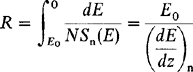 (4-45)
where (dE/dz)n = −NSn(E). In the case of Ar in Cu, (dE/dz)n ![]() 100eV/A. Thus, for every keV of ion energy the altered layer extends about 10 Å (Ref. 13).
100eV/A. Thus, for every keV of ion energy the altered layer extends about 10 Å (Ref. 13).
Through the use of high-energy ion beams, mixing reactions can occur over substantial dimensions. Films can, therefore, be effectively alloyed with substrates, and layered, normally immiscible films can be partially homogenized with the assistance of ion implantation. Such effects are extremely efficient in promoting adhesion of films to substrates, probably the most significant benefit ion bombardment confers on growing films.
4.6.4.4 Amorphization of Films
Perhaps the most extreme form of structural modification is converting a crystalline film into an amorphous one. As we shall see in Section 9.6, materials that are crystalline in bulk form (e.g., metals) can sometimes be deposited as amorphous thin films, but not easily. One route to producing amorphous thin films is to expose crystalline films to an ion beam of appropriate flux and energy. The dose of ions required for amorphization can be roughly estimated assuming that the energy density is essentially the same as that needed for melting. In the case of Si this amounts to about 20 eV/atom, or ∼ 1024 eV/cm3. For ions of energy E0, the dose is therefore
Assuming E0 = 1 keV and RP = 10 Å, φ = 1014 ions/cm2. In practice a dose greater than 1016 ions/cm2 is required, indicating that lattice damage and recrystallization effects occur simultaneously. Greater depths of film amorphization can be achieved through overlapping implants with successively higher-energy ions. Amorphous films are frequently deposited during plasma and ion-beam assisted film-deposition processes. In such cases the critical dose-ion energy requirements for amorphization are exceeded.
4.7 CONCLUSION
This chapter invites comparisons with the previous one and attempts to establish a base for better understanding plasma-assisted film deposition and etching processes in the next two chapters. Such a backward as well as forward perspective can be gleaned from Table 4-3 and Fig. 4-19. Differences in the plasma discharge environment relative to that of a vacuum are compared in Table 4-3. Both are low-pressure environments, but introduction of cathode and anode electrodes and a means of coupling electromagnetic energy to the system partially ionizes the discharge gas. The disproportionate role played by this relatively small concentration of electrons and ions is responsible for the gas-phase discharge structure, sustained ionization, and the varied dynamical motion of these species in electric and magnetic fields. Many of the effects described in the chapter arise from the fact that electrons travel faster and are more energetic than ions. Furthermore, electron collisions with reactive gases create metastable species that promote plasma-assisted chemical reactions. Central to thin-film deposition processes is the ion bombardment of cathodes. Upon impact, a train of events is initiated resulting in the ejection or sputtering of atoms from them. Critical in this regard is the sputter yield, the property that determines how efficient the process is. Once ejected, these atoms fly through the intervening plasma where they deposit sequentially at the substrate (anode). Here again ion bombardment plays a beneficial role, this time to modify the structure and composition of the growing films.
Table 4-3 Vacuum/Evaporation vs Plasma/Sputtering
| Vacuum/evaporation | Plasma/sputtering | |
|---|---|---|
| A. Source attributes | ||
| 1. Phase | Melt or solid | Solid target |
| 2. Mechanism of atom removal | Thermal evaporation (hot source) | Ion bombardment and collisional momentum transfer (cool target) |
| 3. Energy supplied to source | Thermal energy ∼ 0.1 to 0.2 eV/atom + ΔHV | > 20 eV/atom |
| 4. Atom removal rate | ∼ 1.3 × 10¹⁷ atoms/cm2-s for M = 50, T = 1500 K, Pe = 10−3 torr (Eq. 3-2) | ∼ 1016 atoms/cm2-s at 1 mA/cm2 and S = 2 |
| 5. Atom emission geometry | cos φ and cosn φ | cos φ as well as directional according to crystallography |
| 6. Applicability, availability | All materials, generally high purity | Targets of all materials, variable purity |
| B. Gas phase attributes | ||
| 1. Composition | Evaporant atoms, associated and dissociated compound fragments, residual gases | Sputtered atoms, assorted metastable ionized and excited species, sputtering gas, ions, electrons, residual gases |
| 2. Pressure | High to ultrahigh(∼ 10−5 to 10−10 torr) | ∼ 1-100 mtorr discharge |
| 3. Species energy | ∼ 0.1 – 0.2eV for evaporants | 3–10 eV for sputtered atoms 2–5 eV for electrons |
| 4. Atomic mean free path | Larger than evaporant—substrate spacing. No gas collisions in vacuum | Less than target—substrate spacing. Many gas collisions in the discharge |
| C. Condensed film attributes | ||
| 1. Energy of condensing atoms | Low (0.1 to 0.2 eV) | High (∼ a few eV); higher with substrate bias |
| 2. Gas incorporation | None | Some |
| 3. Adhesion to substrate | — | Generally good |
| 4. Film stoichiometry | Generally different from multicomponent alloy and compound sources | Same as the target composition |
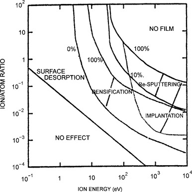
Figure 4-19 Regions of dominance for various ion-bombardment processes as a function of ion/atom ratio and ion energy. Experimental data for different material systems typically fall within the indicated fields. After J. M. E. Harper, J. J. Cuomo, R. J. Gambino, and H. R. Kaufman, in Ion Bombardment Modification of Surfaces: Fundamentals and Applications, eds. O. Auciello and R. Kelley. Elsevier, Amsterdam, 1984.
Consideration of Fig. 4-19 is a way to view these latter ion–surface interactions. In this figure the range over which particular processes dominate are mapped as a function of (charged) ion/(neutral) atom ratio and ion energy. When the ion/atom ratio and ion energy values are both below threshold levels defined by the line with slope equal to −1, ion bombardment simply does not modify film properties. Irrespective of ion energy, desorption of surface impurities occurs at the lowest ion fluxes. However, as the ion/atom, flux ratio increases, film densification and ion implantation become more probable; in general densification proceeds at lower ion energies than those required for implantation. Resputtering effects dominate at the highest flux levels and ion energies. Finally, no film forms if the atom flux is simply too low; in such a case all that happens is ion implantation and sputtering or etching of the substrate.
1. Consider a system containing an ionizable gas that surrounds parallel electrodes with the cathode at x = 0 and anode at x = d, where d > x > 0. A discharge is initiated and the following is assumed:
From this information derive the Townsend equation.
4. Suppose the electron velocity distribution function in a plasma is essentially given by the Maxwell–Boltzmann form of Eq. 2-1, or
5. Rather than a point ionic charge immersed in a plasma consider aplanar sheet of positive ionic charge surrounded by plasma. If Poisson’s equation for this case is
6. In a 13.56 MHz RF plasma operating at a pressure of 250 mtorr, assume Te = 20,000 K.
7. Derive an expression for the time it takes a positive ion to traverse the cathode sheath assuming collisionless motion in a uniform electric field. Calculate this time for an Ar+ ion if the sheath thickness is 0.5 mm and the target voltage is 800 V.
Why is the energy of ion bombardment of the cathode expected to be higher for DC rather than high frequency operation?
8. The electrical conductivity (σ in units of (Ω-cm)−1), or reciprocal of the resistivity of a medium is given by ![]() where ni, q, and μi are the density, charge, and mobility of the charge carriers. Making appropriate assumptions, estimate the electrical conductivity of a 100 mtorr Ar plasma whose electron density is 1010/cm3 and energy is 2.5 eV. How does this value compare to the conductivity of typical metals and semiconductors?
where ni, q, and μi are the density, charge, and mobility of the charge carriers. Making appropriate assumptions, estimate the electrical conductivity of a 100 mtorr Ar plasma whose electron density is 1010/cm3 and energy is 2.5 eV. How does this value compare to the conductivity of typical metals and semiconductors?
10. A simple approximation by Sigmund for the sputter yield when the projectile energy (E) is less than 3 keV is
This relation holds when ![]() where Zp and Zt are the atomic numbers of the projectile and target, respectively. Calculate S for Si bombarded with 500-eV Ar+ ions. Assume the escape barrier energy for Si is 7.8 eV. How does the value of S compare with that of Eq. 4-35?
where Zp and Zt are the atomic numbers of the projectile and target, respectively. Calculate S for Si bombarded with 500-eV Ar+ ions. Assume the escape barrier energy for Si is 7.8 eV. How does the value of S compare with that of Eq. 4-35?
11. A parallel plate plasma reactor with 60 cm diameter electrodes contains argon at a pressure of 20 Pa. The electron temperature is 2 eV while the ion and neutral temperature is 0.03 eV. If the plasma density is 1016/m3calculate:
Are the criteria for a true plasma met in this case?
12. The diode plasma configuration of Fig. 4-1 outwardly resembles the electrochemical cell that is widely used to electrodeposit thin metal films on metallic substrates. What are the differences in the operation of each of these systems? In particular, focus on the distinctions between ionized gases and aqueous electrolytes containing ions, and the dynamics of charge carrier motion between the electrodes.
13. Theory indicates that the kinetic energy (E) and angular spread of neutral atoms sputtered from a surface are given by the distribution function
where US = binding energy of surface atoms, φ = angle between sputtered atoms and the surface normal, and C = constant.
15. Implantation of 1016 phosphorus dopant ions/cm2 into silicon at a energy of 160 keV yields a Gaussian profile with a peak dopant concentration of 4.8 × 10²⁰/cm3, recorded at a subsurface distance of 0.18 μm. At the Si surface the dopant concentration was 3 × 10¹⁹/cm3. What is the dose, projected range, and projected straggle of this distribution?
16. The critical ion/atom (I/A) ratio for the annealing of stress in Ge films by Ar ion bombardment was experimentally determined to obey the relation I/A = 150E−1.59, for values of energy E(eV) between 200 and 2000 eV. At higher energies it was found that I/A = 4760E−2.04 for 2000 eV < E < 5000 eV. Plot these results on Fig. 4-19. How do you reconcile the location of these plots within the overall map?
1 Langmuir I. Phys. Rev.. 1929;33:954.
2 Vossen J.L., Cuomo J.J. Vossen J.L., Kern W. Thin Film Processes. New York: Academic Press, 1979.
3 Sanders D.M. J. Vac. Sci. Technol.. 1989;A7:2339.
4 Chapman B. Glow Discharge Processes. New York: John Wiley & Sons; 1980.
5 Grill A. Cold Plasma in Materials Fabrication. New York: IEEE Press; 1994.
6 Mahan J.E. Physical Vapor Deposition of Thin Films. New York: John Wiley & Sons; 2000.
7 Lieberman M.A., Lichtenberg A.J. Principles of Plasma Discharges and Materials Processing. New York: John Wiley & Sons; 1994.
8 Flamm D.L., Flamm D.L., Herb G.K. Manos D.M., Flamm D.L. Plasma Etching—An Introduction. Boston: Academic Press, 1989.
9 Mattox D.M. J. Vac. Sci. Technol.. 1989;A7(3):1105.
10 Rabalais J.W., Marton D. Nucl. Instrum. Method. 1992;B67:287.
11 Malherbe J.B. Crit. Rev. Solid State Mat. Sci.. 1994;19(2):55.
12 Sigmund P. Phys. Rev.. 1969;184:383.
13 Feldman L.C., Mayer J.W. Fundamentals of Surface and Thin Film Analysis. New York: North Holland; 1986.
14 Lindhard J., Scharff M., Schiott H.E. Mat. Fys. Medd. Dan. Vid. Selsk.. 1963;33:14.
15 Mahon J.E., Vantomme A. J. Vac. Sci. Technol.. 1997;A15:1976.
16 Westwood W.D. Levy R.A., editor. Microelectronic Materials and Processes. Dordrecht, The Netherlands: Kluwer Academic, 1989.
17 Langreid N., Wehner G.K. J. Appl. Phys.. 1961;32:365.
18 Wehner G.K. Maissel L.I., Glang R. Handbook of Thin Film Technology. New York: McGraw-Hill, 1970.
19 Oechsner H. Appl. Phys.. 1975;8:185.
20 Johnson R.E., Sundqvist B.U.R. Physics Today. 1992;45(3):28.
21 Kay E., Rossnagel S.M. Cuomo J.J., Rossnagel S.M., Kaufman H.R. Handbook of Ion Beam Processing Technology. Park Ridge, NJ: Noyes Publications, 1989.
22 Machlin E.S. Materials Science in Microelectronics, The Relationships between Thin Film Processing and Structure. Hastings on Hudson, NY: GIRO Press; 1995.
23 Tsai H., Bogy D.B. J. Vac. Sci. Technol.. 1987;A5:3287.
24 Wehner G.K. J. Vac. Sci. Technol.. 1985;A3:1821.
25 Banks B.A. Cuomo J.J., Rossnagel S.M., Kaufman H.R. Handbook of Ion Beam Processing Technology. Park Ridge, NJ: Noyes Publications, 1989.
26 Kuratani N., Ebe A., Ogata K., Shimizu I., Setsuhara Y., Miyake S. J. Vac. Sci. Technol.. 2001;A19:153.
27 Windischmann H. Crit. Rev. Solid State Mat. Sci.. 1992;17:547.
28 Ohring M. The Materials Science of Thin Films. Boston: Academic Press; 1992.
29 Bradley R.M. Cuomo J.J., Rossnagel S.M., Kaufman H.R. Handbook of Ion Beam Processing Technology. Park Ridge, NJ: Noyes Publications, 1989.
30 Kelly R., Miotello A. Pauleau Y., editor. Materials and Processes for Surface and Interface Engineering. The Netherlands: Kluwer, 1995.