
Logic gates
8.1 Logic gates
Digital electronic logic gates are relatively cheap and readily available as integrated circuits. Such gates find a wide range of applications. For example, they might be used to determine when an input signal control system is to be allowed to give an output, as in an alarm system. Such logic gates are essentially just switching devices and this section considers the basics of such devices.
8.1.1 Switching circuits
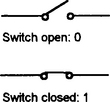
Consider a simple on-off switch (Figure 8.1). If we denote a closed contact by a 1 and an open contact by a 0 then the switch has just two possible states: 1 or 0.
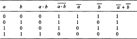
Suppose we have two switches a and b in series. Each switch has two possible states, 0 and 1. Figure 8.2 shows the various possibilities for switches. In (a) both switches are open, in (b) a is open and b is closed, in (c) a is closed and b is open and in (d) a and b are both closed. With (a) the effect of both switches being open is the same as would be obtained by a single open switch; (b) and (c) likewise are equivalent to a single open switch but (d) is equivalent to a single closed switch. Thus we can say that the two elements are equivalent to 0 for (a), (b) and (c) but 1 for (d). In tabular form we can represent the state of the circuit by Table 8.1:Such a table is known as a truth table. If a AND b are 1 then the result is 1. Such an arrangement is known as an AND gate since both a and b have to be 1 for the output to be 1.

Consider two switches in parallel. Figure 8.3 shows the various possibilities for switches. In (a) both switches are open, in (b) a is open and b is closed, in (c) a is closed and b is open and in (d) a and b are both closed. With (a) the effect of both switches being open is the same as would be obtained by a single open switch; (b), (c) and (d) are equivalent to a single closed switch. Thus we can say that the two elements are equivalent to 0 for (a), and 1 for (b), (c) and (d). In tabular form we can represent the state of the circuit by the truth table (Table 8.2):Such an arrangement is known as an OR gate since if a or b is 1 then the result is 1.

Another possible form of switch circuit is where two switches are connected together so that the closing of one switch results in the opening of the other. Figure 8.4(a) illustrates the switch action with (b) showing the upper switch open when the lower switch is closed and (c) the upper switch closed when the lower switch is open. The lower switch is said to give the complement of the upper switch. Table 8.3 is the truth table:Such an arrangement constitutes a NOT switching circuit, since if one switch is 1 then the other switch is not 1.

Logic gates
With a mechanical switch we can represent the two logical states of 0 or 1 as the switch being open and closed. With electronic switches, 0 is taken to be a low voltage level and 1 a high voltage level for what is called positive logic, although the opposite convention (negative logic) can be used with 0 being represented by a high voltage level and 1 by a low voltage level. The 0 and the 1 do not represent actual numbers but the state of the voltage or current. The term logic level is often used with the voltage being said to be at logic level 0 or logic level 1.
The basic building blocks of digital electronic circuits are called logic gates. A logic gate is an electronic block which has one or more inputs and an output. The output can be either high or low depending on the digital levels at the input terminals. The following sections take a look at the logic gates: AND, OR, INVERT/NOT, NAND, NOR and XOR. Different sets of standard circuit symbols have been developed in Britain, Europe and the United States; an international standard (IEEE/ANSI) has, however, been developed based on squares. In this text, both the IEEE/ANSI form and the older United States form are shown.
The AND gate gives an output 1 when both input A and input B are 1. Figure 8.5 shows the symbol, the associated truth table being given in Table 8.4

The OR gate gives an output 1 when either input A or input B is 1. Figure 8.6 shows the symbol and Table 8.5 the truth table.

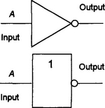
The INVERT or NOT gate has a single input and gives a 1 output when the input is 0. The gate inverts the input, giving a 1 when the input is 0 and a 0 when the input is 1. Figure 8.7 shows the gate symbol and Table 8.6 gives the truth table.
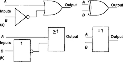
This gate (Figure 8.8) is logically equivalent to a NOT gate in series with an AND gate, NAND standing for NotAND. The symbol for the gate is the AND symbol followed by a small circle, the small circle being used to indicate negation. The gate has the truth table shown in Table 8.7. There is a 1 output when A and B are both not 1, i.e. are both 0.

This gate (Figure 8.9) is logically equivalent to a NOT gate in series with an OR gate. It is represented by the OR gate symbol followed by a small circle to indicate negation. Table 8.8 gives the truth table, there being a 1 output when neither A nor B is 1.

The OR gate gives an output 1 when either input A or input B is 1 or both A and B are 1. The EXCLUSIVE OR gate gives an output 1 when either input A or input B is 1 but not when both are. Figure 8.10 shows the gate symbol and Table 8.9 the truth table.
By combining gates it is possible to generate other switching operations. This is illustrated in the following example and discussed later in this chapter.
Suppose we wanted to design a switching circuit in order to operate a relay from a combination of four switches so that the relay is energised when switch 1 and switch 2 are both closed, or when switch 3 and switch 4 are both closed, or when switch 1 and switch 3 are both closed. Design a system of logic gates which would give this.
The output required is when we have (S1 and S2) or (S3 and S4) or (S1 and S3). Figure 8.11 shows how this may be realised with gates.

Programmable logic controllers (PLCs) use a simple form of programming in order to exercise control functions. This program involves drawing each step in a program as the rung on a ladder, each rung then being taken in turn from top to bottom. Each rung can execute logic switching functions such as AND and OR. Figure 8.12(a) shows the symbols used to represent normally open switches, normally closed switches and output devices. Figure 8.12(b) shows three rungs in a ladder program. With rung 1 we have an AND gate situation in that both A and B have to be on for there to be an output. With rung 2 either A or B have to be on for there to be an output and so we have an OR gate. Rung 3 shows a NOT gate in that when A has an input it switches the output off.

8.2 Boolean algebra
In this section we look at how we can develop algebraic notation and rules to describe and manipulate logic gate arrangements.
Notation
For the AND operation, i.e. the series connections of switches a and b, a is considered to be multiplied by b. Generally • is used for the multiplication symbol. From truth Table 8.4 we thus have the rules:
For the OR operation, i.e. the parallel connection of switches a and b, a is considered to be added to b. From truth Table 8.5 we have the rules:
For the NOT operation, i.e. the complement with the switches, we use a bar over a symbol to indicate NOT. Thus truth Table 8.6 gives the rules:
Boolean algebra
The binary digits 1 and 0 are the Boolean variables and, together with the operations ⋅, + and the complement, form what is known as Boolean algebra. By constructing the appropriate truth tables the following laws can be derived:
• Anything ORed with itself is equal to itself
See Table 8.10.
• Anything ANDed with itself is equal to itself
See Table 8.11.
• Input sequence for OR and AND
It does not matter in which order we take the inputs for OR and AND gates, the output is the same. This is illustrated by Table 8.12 for OR.
As Table 8.13(a) indicates:
Table 8.13(a)

As Table 8.13(b) indicates.
Table 8.13(b)
Anything ORed with its own negative is 1. See Table 8.14.
Table 8.14

Anything ANDed with its own negative is 0. See Table 8.15.
Table 8.15

Anything ORed with a 0 is equal to itself, anything ORed with a 1 is equal to 1. See Table 8.16.
Table 8.16
| a | a+0 | a+1 |
| 0 | 0 | 1 |
| 1 | 1 | 1 |
Anything ANDed with a 0 is equal to 0, any thing ANDed with a 1 is equal to itself. See Table 8.17.
Table 8.17
| a | a·0 | a·1 |
| 0 | 0 | 0 |
| 1 | 0 | 1 |
De Morgan laws:
• The complement of the outcome of switches a and b in parallel, i.e. an OR situation, is the same as when the complements of a and b are separately combined in series, i.e. the AND situation. Table 8.18 shows the validity of this.
Table 8.18

• The complement of the outcome of switches a and b in series, i.e. the AND situation, is the same as when the complements of a and b are separately considered in parallel, i.e. the OR situation. Table 8.19 shows the validity of this.
Table 8.19
Using the rules given above, complicated switching circuits can be reduced to simpler equivalent circuits.
The operation of an output relay controlled by a PLC program is given by the Boolean expression:
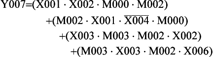
(a) Represent this expression as rungs in a PLC ladder program, with a rung for each part of the expression.
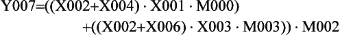
(b) Simplify the ladder program and hence write another Boolean expression which describes the simplified program.
(a) Each bracketed term can be represented by a rung in a ladder program and so give the program shown in Figure 8.13(a).
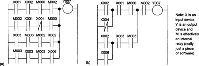
(b) Figure 8.13(b) shows how we can simplify the ladder program and still give the same outcome. Such a program can then be described by the Boolean expression:
8.3 Logic gate systems
The operations ·, + and the complement can be used to write the Boolean functions for complex switching circuits, the states of such circuits being determined by developing the truth table to indicate all the various switching possibilities. Boolean algebra might then be used to simplify the switching circuits.
Write, for the circuit shown in Figure 8.14, (a) the truth table and (b) the Boolean function to describe that truth table.

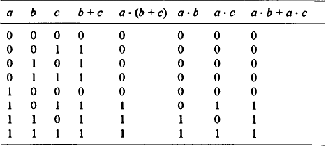
(a) a and b are in series, and in parallel with the series arrangement of c and d. The result of using the switches is that only when either a and b are closed or c and d are closed will there be an output. Table 8.20 shows the truth table.

(b) The Boolean function for the two switches a and b in series is a · b, the AND function, and thus, since the function for two items in parallel is OR, the function for the circuit as a whole is:
Derive the Boolean function for the switching circuit shown in Figure 8.15.

In the upper parallel arm of the circuit, the switches a and b are in series and so have a Boolean expression of a · b. In the lower arm the complements of a and b are in series. Thus the Boolean expression for that part of the circuit is ![]()
Because the two arms are in parallel the expression for the parallel part of the circuit is ![]()
In series with this is switch c. Thus the Boolean function for the circuit is: ![]()
Combining gates
By combining logic gates it is possible to represent other Boolean functions and use of Boolean algebra can often be used to simplify the arrangement.
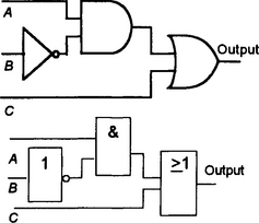
Determine the Boolean function describing the relation between the output from the logic circuit shown in Figure 8.16. Hence, consider how the circuit could be simplified.

This might be a circuit used with a car warning buzzer so that it sounds when the key is in the ignition (A) and a car door is opened (B) or the headlights are on (C) and a car door is opened (A). We have two AND gates and an OR gate. The output from the top AND gate is A · B, and from the lower AND gate C · A. These outputs are the inputs to the OR gate and thus the output is
The circuit can be simplified by considering the Boolean algebra. Using equation [9] the Boolean function can be written as:
We now have A and B or C. This function now describes a logic circuit with just two gates, an OR gate and an AND gate. Figure 8.17 shows the circuit.

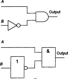
Devise a logic gate system to generate the Boolean function ![]()
A · B requires an AND gate, but as the B input has to be inverted we precede the input from B to the AND gate by a NOT gate. We then require an OR gate for the output from the AND gate and C. Figure 8.18 shows the gate system.
Boolean function generation from truth tables
Often the requirements for a system are specified in terms of a truth table and the problem then becomes one of determining how a logic gate system can be devised, using the minimum number of gates, to give that truth table. The forms to which most are minimised are an AND gate driving a single OR gate or vice versa.
Two AND gates driving a single OR gate (Figure 8.19(a)) give, what is termed, the sum of products form:
Two OR gates driving a single AND gate (Figure 8.19(b)) give, what is termed the product of sums form:
The usual procedure to find the minimum logic gate system is thus to find the sum of products or the product of sums form that fits the data. Generally the sum of products form is used. The procedure used is:
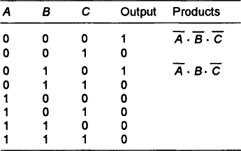
1. Consider each row of the truth table in turn that generates a 1 output and find the product that would fit a row. Only a row of a truth table that has an output of 1 need be considered, since the rows with 0 output do not contribute to the final expression. For example, suppose we have a row in a truth table of: A = 1, B = 0 and output = 1. When A is 1 and B is not 1 then the output is 1, thus the product which fits this is:
2. The overall result is the sum of all the products for the rows giving 1 output.
Determine a logic gate system to give the following truth table.

we only need consider the third row, thus the result is:
The logic gate system that will give this truth table is thus that shown in Figure 8.20.
A PLC and a central heating system
Consider a domestic central heating system (Figure 8.21) and its control by a PLC (see earlier Maths in Action in this chapter). The central heating boiler is to be thermostatically controlled and supply hot water to the radiator system in the house and also to the hot water tank to provide hot water from the taps in the house. Pump motors have to be switched on to direct the hot water from the boiler to either, or both, of the radiator and hot water systems according to whether the temperature sensors for the room temperature and the hot water tank indicate that the radiators or tank need heating. The entire system is to be controlled by a clock so that it only operates for certain hours of the day. Figure 8.22 shows how a PLC might be used and its ladder program.


The boiler, output Y430, is switched on if X400 and X401 and either X402 or X403 are switched on. This means if the clock switched is on, the boiler temperature sensor gives an on input, and either the room temperature sensor or the water temperature sensors give on inputs. The motorised valve M1, output Y431, is switched on if the boiler, Y430, is on and if the room temperature sensor X402 gives an on input. The motorised valve M2, output Y432, is switched on if the boiler, Y430, is on and if the water temperature sensor gives an on input.
Design a PLC ladder program that will control a simple red–amber–green traffic light sequence for two inputs X0 and X1 to give the outputs Y0, Y1 and Y2 (Figure 8.23) shown in the following table:
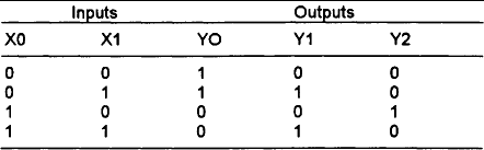
Note: logic 0 defines an open switch or a light turned OFF, logic 1 defines a closed switch and a light turned ON.

Figure 8.24(a) shows how we can represent the above truth table by a logic gate system and Figure 8.24(b) by rungs in a ladder program.
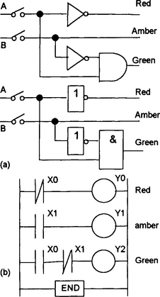
When there is no input to X0 then the red light is ON. Thus, when the input to X0 is 0 then, as the switch is normally closed, the output Y1 is ON; when the input is 1, to open the switch, then the output is OFF.
Karnaugh maps
The Karnaugh map is a graphical way of representing a truth table and a method by which simplified Boolean expressions can be obtained from sums of products. The Karnaugh map is drawn as a rectangular array of cells with each cell corresponding to the output for a particular combination of inputs, i.e. a particular product value. Thus, Figure 8.25(a) shows the four-cell box corresponding to two input variables A and B, this giving four product terms. We then insert the function for each input combination, Figure 8.25(b) showing this for an AND gate and Figure 8.25(c) for an OR gate. Figure 8.26 shows how we can represent such maps with input labels A and B for 1 entries and not A and B for 0 entries.


Karnaugh maps not only pictorially represent truth tables but also can be used for minimisation. Suppose we have the following truth table:
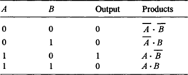
Figure 8.27 shows the Karnaugh map for this truth table with just the 1 output shown. On the map this entry is just the cell with the coordinates A = 1, B = 0 and so gives the indicated product. The Karnaugh map enables the minimisation to be spotted visually.

As a further example, consider the following truth table:

Figure 8.28 shows the Karnaugh map for this truth table with just the 1 output shown. This has an output given by:
This can be simplified to:
Thus we have a rule for the map that: when two cells containing a 1 have a common edge then we can simplify them to just the common variable, the variable that appears in the complemented and uncomplemented form is eliminated. To help with such simplifications, we draw loops round Is in adjacent cells. Note that in looping, adjacent cells can be considered to be those in the left- and right-hand columns. Think of the map as though it is wrapped round a vertical cylinder and the left- and right-hand edges of the map are joined together. There are other rules we can develop, namely: looping a quad of adjacent 1s eliminates the two variables that appear in complemented and uncomplemented form and looping an octet of adjacent 1s eliminates the three variables that appear in both complemented and uncomplemented form.
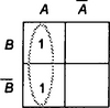
Figure 8.29(a) shows how we can draw a Karnaugh map for three inputs and Figure 8.29(b) for four inputs. Note that the cells are labelled so horizontally adjacent cells differ by just one variable, likewise adjacent vertical cells.

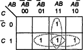
Determine the simplified Boolean expression for the Karnaugh map shown in Figure 8.30.
Determine the simplified Boolean expression for the Karnaugh map shown in Figure 8.31.

We have a doublet loop and a quad loop and so the outcome is:
Problems 8.3
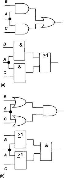
1. State a Boolean function that can be used to represent each of the switching circuits shown in Figure 8.32.

2. Give the truth tables for the switching circuits represented by the Boolean functions:
3. Determine the Boolean functions that could generate the outputs in Figure 8.33.

4. Give the truth table for the switching circuit corresponding to the Boolean function:
5. Draw switching circuits to represent the following Boolean functions:
6. Determine the Boolean equations describing the logic circuits in Figure 8.34, then simplify the equations and hence obtain simplified logic circuits.

7. Draw switching circuits to represent the Boolean functions:
8. Derive the Boolean functions for the truth tables in Table 8.21(a) and (b).
Table 8.21(a)

Table 8.21(b)

9. Determine the Boolean equations describing the logic circuits in Figure 8.35, then simplify the equations and hence obtain simplified logic circuits.

10. For the Karnaugh maps in Figure 8.36, produce the simplified Boolean expression.
