
Interface Devices
This book is primarily concerned with embedded control. That is, a microprocessor-based system which is dedicated to a limited range of tasks, such as washing machine control, traffic light operation, credit card verification, etc. This chapter looks at the electrical characteristics of typical I/O devices.
Single Line Input
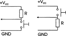
Switches come in two varieties: toggle (latching) and momentary (non-latching). Most microprocessor systems use momentary inputs. This is intentional so that upon a power failure, the system returns to a known state prior to the next power-up.
The switch consists of a pair of contacts, one of which has either a pull-up resistor or a pull-down resistor as illustrated in Figure 4.1. The signal is either normally-high switching low or normally low switching high. TTL does not respond very well to pull-down resistors, so most systems use a pull-up scheme regardless of the actual technology (i.e. CMOS or TTL).

This is polled software which will cause either version to relocate to a piece of code with the label ‘routine’ if the button is being pushed when the input line is being sampled (= polled). An interrupt driven version is sometimes more appropriate if there are many possible inputs or the processor has several tasks to do.
The 8051 has vectored interrupts and provided that one of the two External Interrupt lines is used for the push-button, then the code will automatically relocate to the handling routine.
The External Interrupt vector is either location 0003 for X0 or 0013 for X1. These locations are specific to external interrupts and the location would normally contain a jmp instruction to access the Interrupt Service Routine.
The PIC16C5x family has no interrupts, and the others have no vectoring capability. Hence the code would be slightly more complicated while the location of the External Interrupt handler is determined.
The PIC relocates to address 04 when an interrupt occurs and interrupts have been enabled. If there is only one source of interrupt enabled, then location 04 could contain a simple GOTO to access the Interrupt Service Routine. If more than one interrupt source is enabled then the code at location 04 needs to ascertain which of the sources caused the interrupt before it GOs TO the appropriate service routine.
Both 8051 and PIC families have options for internal passive resistors on some I/O ports which will perform the pull-up function.
Optocouplers
One problem with switches is that as the contacts make, they tend to bounce under the force of the impact. This contact bounce can last for longer than 20 ms. The effect would be seen as a series of narrow pulses which occurred every time the switch was pressed. If it was part of a counting mechanism, then this would represent a serious source of error. Hardware solutions to the problem vary from discrete ‘debouncers’ which can be constructed from two logic gates to dedicated switch debouncing ICs. When the design includes a microcontroller, then a good alternative is to use software debouncing, i.e. to use software to discriminate between a bouncing input and frequent button pushes. The usual technique is to detect the first transition and then to wait for a short period before testing again.
Some inputs may come in the form of opto interrupters. The number of revolutions or angular velocity can be counted with the aid of a slotted rotary disc. Opto devices are inherently bounce free so the software interface is relatively simple to achieve, especially if software interrupts are to be used.
Sometimes it is important to detect the direction of rotation. If so, a quadrature detector made from two closely aligned opto switches, as in Figure 4.2, may be used.

With this system, both speed and direction can be determined: speed by starting an internal Timer/Counter when the first hole is exposed and letting it run until the next hole is uncovered (allowing for a very slow/stopped disc, of course) and direction by comparing the relative transitions of the two signals as they arrive at the sensors.
Single Line Output
This is the most common output style, and can be used as a signal for anything from lighting LEDs (or incandescent lamps), operating motors, unlocking doors, turning on heaters – the list is endless. The basic concept is simple. The output line switches on a higher current device such as a relay, power transistor or triac to control the actual load.
As with any switching circuit, care must be taken when driving inductive loads. Sudden interruption of current through an inductor causes a very large EMF to be induced – the size of which is dependent on the switching speed, but is certainly large enough to destroy the switching device. The conventional solution to this problem is to use a diode in parallel with the load. This is the so-called ‘flywheel’ ‘catching’ or ‘back-EMF’ diode as in Figure 4.3. It prevents the voltage at the lower end from rising more than 0.7 V above the supply voltage. Use it.


Toggling (changing state) can be obtained with the following code:
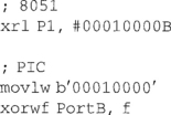
It uses the fact that the exclusive-OR operation changes a bit state if the mask bit is 1, while leaving it unchanged if the mask bit is 0. In these examples, the bit 4 is to be toggled.
The truth table of an exclusive-OR gate is, of course:
| A | B | X |
| 0 | 0 | 0 |
| 0 | 1 | 1 |
| 1 | 0 | 1 |
| 1 | 1 | 0 |
When one of the bits is ‘1’, the exclusive OR changes the state of the other bit. For more detail, see Appendix B.
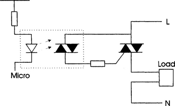
To avoid difficulties with switching inductive loads, it is often worthwhile isolating the microcontroller from the load with an opto-isolator as was seen with the input signals. The load can operate from completely different power supplies than the microcontroller, offering both protection against switching transients and dangerous voltages. (There is still an issue of switching transients on the load side of the circuit. It is illegal to generate Radio Frequency Interference above certain levels and so care must still be taken. There are many cases where inadvertent interference has caused catastophic and tragic failures of nearby electrical/electronic equipment.) The simple opto triac circuit of Figure 4.4 can be used to drive some AC loads, but there is still the possibility of switching transients.
AC Control
A better solution is to use a zero-crossing detector which turns on the AC power when the mains supply is at its lowest. Separate integrated circuits are available for this, and if there is one spare input line on the microcontroller, then it is quite capable of detecting this event all by itself. The circuit of Figure 4.5 would suit.
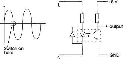
The reverse breakdown voltage of an LED is of the order of 5–10 V. Hence, when the supply reverses, the Junction Diode conducts and limits the reverse LED voltage to approximately 0.7 V. If a pulse is required on both zero crossing points (i.e. when the supply passes from negative to positive and positive to negative) then there would be TWO LEDs connected back-to-back. Care must be taken with the resistor power rating, since it has to drop a large voltage while passing the diode currents.
In each case, a short delay is introduced to ensure that the triac is fully turned on. This will depend on the triac load. If the processor is involved with other tasks, then it would be more appropriate to use the zero crossing input to drive an interrupt routine as it may ‘miss’ the zero crossing pulse.
Burst Mode Control
A variation of this allows for ‘burst mode’ control to vary the amount of power delivered to a load. It is a technique normally reserved for heating loads where the time constants involved are relatively slow. The amount of power delivered is varied by the number of complete cycles of the mains supply in a fixed period. Figure 4.6 shows the principles.
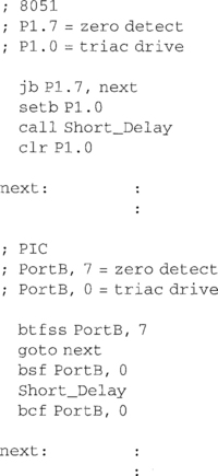
Phase Control
To control the amount of AC power supplied to a load the alternative technique of phase control is used. This can cause radio frequency interference problems, but is a common technique for dimming (incandescent) lamps and controlling the speed of universal motors. The microcontroller must sense the zero-crossing point and then apply a time delay before turning the triac on. Figure 4.7 shows typical waveforms.

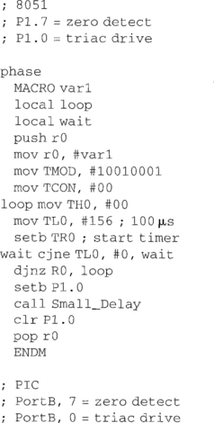
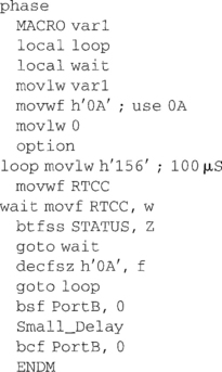
Both macros take as a parameter the number of 100 μs units before the triac is to be turned on. (Of course, the timing depends on the clock chosen. It is assumed here that the 8051 is operating from a 12 MHz clock and the PIC from a 4 MHz clock.) The UK mains is at 50 Hz and the half-wave period is thus 10 ms. There would be 100 × 100 μs subdivisions of the half-wave waveform. This should be enough for all practical purposes of phase control. The useful range of parameters taken by the macro would be 1–99. This parameter is passed to a register which is decremented to control the number of 100 μs iterations.
Keypad Input
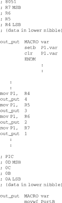
This is a cover-all name for a group of keys usually with a related function. Common sizes have 12 or 16 keys but there is no upper or lower limit. Section 1 showed that each key needs 1 data line to interpret it. Using 16 lines to indicate which of the keys on a keypad had been pressed is a wasteful use of resources. One improvement is called scanning and can be achieved in software, but is often left to a separate, dedicated IC. The procedure for scanning is as follows. Imagine the keys are arranged in a square array. Each (momentary) switch has two electrical contacts. One of these is connected to a common horizontal (ROW) connection and the other to a common vertical (COLUMN) connection. One at a time, each column line is changed from ‘0’ to ‘1’ and back to ‘0’. While it is high, the rows are examined, one at a time, to see if the ‘1’ can be detected, and if so, on which line. By knowing which row and which column circuit was active at the time, the individual key pressed can be identified. This process is called multiplexing. Using software scanning, a 4 × 4 keypad would require 8 I/O lines as in Figure 2.10 in the 8051 section.
Many applications opt for a dedicated IC such as the 74C922 in Figure 4.8. This would need only 5 lines connected to the microcontroller. These are called A, B, C, D and DA. A, B, C and D are binary data lines which indicate which key was pressed. DA is the Data Available line (active high) which indicates that a key is being pressed.

The advantages of the dedicated IC are that:
The binary code is not related to the indicated value on the key cap if a standard keypad is used. In this case, a software ‘lookup table’ must be used to convert returned code to intended value. One unfortunate characteristic of this IC is that the polarity of the DA pin is not suitable for driving the Interrupt line of the microcontroller. So, unless another logic device is available, or a simple 1-transistor inverter is used, the DA line must be polled to see if a valid key is being pressed.
Keyboard Input
Keyboards can have 102 keys or more, and the special encoder ICs usually work on an 8-bit data bus. These can be interfaced to microcontrollers relatively easily, but knowledge of the bus protocols and signal transfer levels is needed. These can be obtained from the manufacturers’ data sheets. Alternatively, they can be treated exactly like a keypad encoder, but with a wider data field.
Seven-segment Displays
This is a common method of numerical display. They are invariably driven by binary (or BCD) to seven-segment display encoder ICs. Each display requires 4 bits. (LED displays can either be common anode or common cathode as in Figure 4.9. There is very little practical difference between them, other than the choice of the correct decoder.)

If several displays are required, then it would be inefficient to use four lines for each. A better structure would be to use a latching binary (BCD) to a seven-segment decoder driver such as a CMOS 4511 and a multiplexing technique, i.e. the four binary input lines would be connected to ALL the display drivers in parallel as in Figure 4.10. If there were to be (say) four displays then we would need four Latch Enable (LE) lines. To display the number ‘6789’ on the display:

1. Output 6, operate LE for chip 1.
2. Output 7, operate LE for chip 2.
A four-digit seven-segment display could be driven in this way by eight output lines.
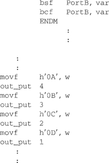
With larger tables, it would probably be more effective to use an auto-increment into a lookup area of RAM. However, with only four elements, there is not much to be gained.
The PIC is capable of sourcing up to 40 mA and sinking up to 50 mA. It is possible to use a single PIC to replace the circuit shown if high efficiency (low current) displays are used. The stobing/multiplex driving of the digits would need to be at a frequency so that the flicker would not be visible. 1–10 kHz is not uncommon in a technique which is often used to drive LED displays.
The attraction of this scheme is only that a PIC has relatively high current drive capability and is very cheap. If the display-PIC is to be driven by another microprocessor, then in all probability, a serial communication method might be more efficient. This would need to be a fast burst of data, otherwise the pause in the display would be noticable while the serial port is being serviced.
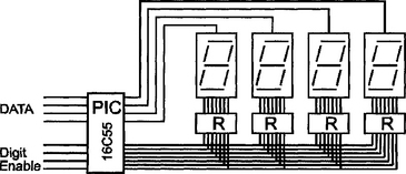
Figure 4.11
Liquid Crystal Displays
Numeric displays can be easily produced with seven segments. If full alphanumeric display is required, then the dot matrix layout is more appropriate. Each character is encoded in a rectangular region of dots. 8 × 5 or 10 × 8 are common formats as in Figure 4.12. Companies such as Hitachi produce dedicated ICs which will drive these displays and they are usually integrated with the LCD so that the designer has only to decide on the layout of the display. Typical formats are

The character sets can be standard or customized.
Graphical displays are also available if pictures rather than text are required, although the software drive for these would obviously be more complex.
The interface requirements vary, but for the simple text displays:
• 4 or 8 data lines (software selectable)
• 3 control lines (although a minimal write-only control can use just 2 control lines.
Chapter 6 shows in more detail the driving details of Liquid Crystal Modules.
Analogue Input
Some microcontrollers have built-in ADCs – for example, the Intel 80552 and PIC16C71. If not provided internally, then a discrete IC must be used externally. Earlier ADCs presented their outputs in a parallel format and use 2 or 3 control or status lines. Most ADCs present their outputs in parallel and have 2 or 3 control or status lines. This is usually a variation on:
| → | SC | start conversion |
| ← | EOC | end of conversion |
| → | OE | output enable |
More recent devices try to align the timing of the control signals with those of the microprocessor itself. So, for example, the ADC0803 can interface directly to many microprocessors; including the 8051 family. The only separate pin is the Chip Select CS which is derived from an address decode or I/O Port pin.
The ADC0803 8-bit Analogue to Digital Converter with Differential Inputs
The ADC0803 is a CMOS 8-bit successive-approximation analogue to digital converter. It is designed to operate from common microprocessor control buses with the three-state output latches driving the data bus. When dealing with microcontrollers, some of these control bus functions have to be provided explicitly by the I/O pins.
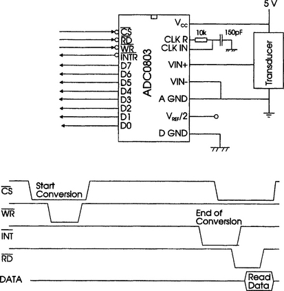
The devices can operate with an external clock signal or, with an additional resistor and capacitor, using an on-chip clock generator.
If circuit board space is at a premium, and a microcontroller with inbuilt ADCs is not available, then a SERIAL ADC may be a solution. This device converts the analogue signal to digital and then outputs it one bit at a time in a serial fashion. The microcontroller controls the rate of output using a ‘data clock’ signal to the ADC.
The PIC family is not designed for external memory mapped devices, so the most convenient way to access an ADC is via a serial control medium. The alternative (parallel conversion) would take up the other valuable PIC resource of I/O lines. Serial conversion does seriously limit the rate at which conversion can take place, since it takes a finite time to pass the converted data across to the PIC. However, there are many applications for which the device is suitable.
TLC548 8-bit Analogue to Digital Converter with Serial Control
The TLC548 A/D peripheral integrated circuit is built around an 8-bit switched capacitor successive approximation ADC. It is designed for serial interface with a microprocessor or peripheral through a 3-state data output and an analogue input. It uses only the Input/Output clock (I/O clock) input along with the Chip Select (/CS) input for data control. The maximum clock input frequency of the TLC548 is guaranteed up to 2.048 MHz. Figure 4.14 shows the interface and timing diagram of the device.

Multiple Output ADCs
If more channels are needed, try something like the MAXIM MAX146 which offers 8 × 12 bit analogue inputs, and yet still uses a serial interface. The microprocessor not only has to start the conversion and retrieve the data, but also specify which of the channels it requires the data from.
Analogue Output
The ‘simple’ method of achieving this in microcontrollers is via a PWM (pulse width modulated) output. This is available explicitly in some devices, or can easily be implemented with software. The idea is that the output is a pulse train with a mark:space ratio proportional to the desired analogue output, as shown in Figure 4.17. Passing the signal through a simple filter will reconstitute the signal as an analogue voltage. If a faster response is required, then a dedicated DAC might be considered necessary. This device will probably need 8 (or 10 or 12 or 14 or 16) bits of input as well as precision voltage references on the analogue side.
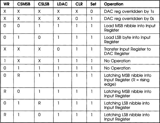
The MAX501 is a 12-bit, 4-quadrant voltage output multiplying digital to analogue converter. It is easily interfaced with microprocessors. Data is transferred into the input register in a right-justified 8 + 4 format. Table 4.1 defines the operations available.
Table 4.1

Motor Drive Circuits
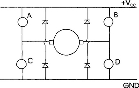
These are best understood by thinking of them as having four coils which must be sequentially energized to drag the rotor around as in Figure 4.16. The normal energization of the coils would be in the sequence A AB B BC C CD D DA. This is easy enough, but direct software control can be complicated by the need to accelerate and decelerate the rotor carefully to avoid ‘rotor slip’. In practice, of course, there are many more steps to one revolution for a stepper motor. Common step values are 0.9°, 1.8° and 3.6°.

If the electrical interface has been set up to be coil A = bit 0, coil B = bit 1, coil C = bit 2 and coil D = bit 3, then using the bit output techniques already described, the software should output the data in the sequence:
| 00000001 | 00000100 |
| 00000011 | 00001100 |
| 00000010 | 00001000 |
| 00000110 | 00001001 |
Between each step there should be a delay which gives the motor mechanics time to react to the output drive from the microcontroller.
DC Unidirectional
A simple relay or transistor can be used to turn the motor on and off. Speed control can be obtained via PWM (pulse width modulation) as already discussed and shown in Figure 4.17.
DC Bidirectional (reversible)
The ‘standard’ way of producing this is with an ‘H’ bridge as in Figure 4.18. One direction is obtained by turning on devices A and D. The opposite direction is obtained by turning on devices B and C. This is common topology for servo mechanisms.
The electronics can be discrete devices or a special purpose IC. These are easier to use and often have suppression and level shifting electronics built in.
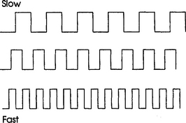
AC Motors
Most AC motors rotate at a speed determined by the frequency of the electricity supply. With software, it is relatively easy to produce a variable frequency square wave as in Figure 4.19. Unfortunately, the square waves have a large harmonic content and this can cause heating and EMC difficulties. The efficiency is improved and the harmonic content decreased if a pseudo-sine wave is generated. Figure 4.20 shows a simplification of a pseudo sinewave. In practice, a real wave of this form would take many pulses to make the transistion from maximum positive to maximum negative. In software terms, this is quite fiddly to generate. The pulse repetition is fixed at a frequency above the normal human hearing limits. The pulse width depends on the amplitude of the sine wave at that point in the cycle. The most sophisticated type of control compensates for the fact that as the psuedo sine wave frequency gets lower, the magnetic circuit of the motor to be controlled can go into saturation – an undesirable situation. This is solved by reducing the apparent amplitude of the psuedo sine wave, i.e. all the pulse widths are reduced by a constant percentage so the filtered (averaged) sine wave output has a lower peak value. This would have to be tailored to each size/rating of motor to be controlled.
Questions
1. Design a software based switch debounce in both 8051 and PIC assembly language so that a single (bouncing) press-and-release of a momentary push button latches an output ON, while a second (bouncing) press-and-release latches the same output OFF. (As described on page 113, when a switch makes, the contacts can bounce for up to 20 ms; leading to false counts in digital circuitry.)
2. Design a solution the quadrature detector on page 115 which has two inputs for the optocouplers and two outputs – FORWARD and REVERSE. The software for 8051/PIC should detect
• if the wheel is stopped, in which case neither of the F or R outputs should be ‘1’;
• the direction of rotation, in which case the appropriate output should be ‘1’.
3. Write a software 8051/PIC MACRO which takes a parameter in the range 0–10. This parameter is to control the percentage of power delivered in a burst mode heating scheme. Assume that a zero-crossing pulse is available at one of the inputs and the output should be a 2 ms pulse from an output immediately after the zero crossing input if the software determines that an output is appropriate. A parameter of 7 should output 14 outputs (i.e. 7 positive and 7 negative half cycles, followed by a non-output for the next 3 cycles (6 half cycles)).
4. Re-write the phase control MACROs for the US 60 Hz supply frequency.
5. It is a curious fact that the dedicated keypad switch IC 74C922 is more expensive than an unprogrammed 16C54. Write a PIC program to emulate the operation of this device.
6. Write a program for the PIC/8051 which has as its inputs a square wave clock and a single bit direction control and four coil drivers as outputs. Design a stepper motor driver. (An advance of this program would add the authenticity that a step increase in input frequency is not instantly matched by an output change, but by the output ramping up to the new frequency.)
7. Write a PIC/8051 MACRO to take an 8-bit value as an input parameter and to output a 1 kHz pulse stream, the pulse width of each is proportional to the input value.