The PIC Microcontroller
Early PIC Variants
The PIC 16 family of microcontrollers was developed by Microchip Technology Inc. in the late 1980s. They are all 8-bit microcontrollers with on-chip CPU, memory and I/O (Input/Output). The original base devices were:
However, this basic range has been supplemented by many and various versions which offer a comprehensive set of CPU, memory and I/O variants.
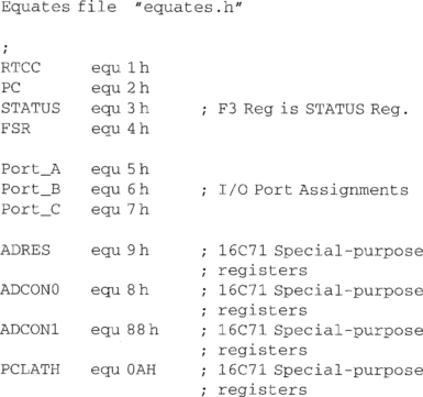
One very useful range of devices for embedded applications is the PIC12C5xx. This is a range of 8-pin Dual In Line ICs which offer all the same facilities as the PIC16C5x but in a smaller package. There are many occasions when a small device is needed for switching, control or timing which does not need a huge amount of I/O lines (in this case, a maximum of 6), but is valued simply because it does not take up a large amount of board space or complexity of interfacing. For additional simplicity, it can be configured to operate from an internal RC oscillator which operates at approximately 4 MHz. Figure 3.2(a) shows the pinout of a PIC12C5xx.

At the other end of the scale, the 40-pin PIC18Cxxx is sold as a high performance RISC CPU with the capability of using a large program address space. Figure 3.2(b) shows the pinout of the PIC18Cxxx. As can be seen, and as is typical of complex, multifunction microcontrollers, the functions of the pins vary according to the application. This can sometimes lead to disappointment, since although the specification sheet lists an impressive array of capabilities of the device, they are not always available concurrently.
• Power on reset. Under most operating conditions, the microcontroller will go to a known RESET condition without the use of external circuitry. However, for ultra-reliable reset operation, a capacitor can be connected to the MCLR (reset) pin.
• Oscillator start-up timer. Internal circuitry holds the microcontroller RESET for approximately 18 ms after the master clear is released.
• Watchdog timer. A technique which, when used, allows the processor to escape from an endless loop fault condition if the watchdog timer is not regularly reset.
• Security EPROM fuse for code protection. When set, the security fuse prevents the internal program memory (the user program) from being read by external devices.
• Power saving SLEEP mode. A software command which shuts the processor down until it is RESET once more.
• EPROM selectable oscillator options. The microcontroller needs a frequency reference from which to operate; this could be chosen from RC components, quartz crystals or ceramic resonators. The oscillator section is hardware optimized to operate from 1 of 4 reference types. The following letters are the suffixes which are used:
| Low cost RC oscillator | :RC |
| Standard crystal/resonator | :XT |
| High speed crystal/resonator | :HS |
| Power-saving low-frequency crystal | :LP |
The CMOS semiconductor technology provides the following:
• Fully static design. If required, the clock can be stopped at any instant, and all data is held in the device memories. It is in effect frozen. Once the clock is restarted, it picks up from where it left off.
• Wide operating voltage range
| 2.5–6.25 volts | 16C5x |
| 3.0–6.0 volts | 16C71 |
| 2.0–6.0 volts | 16C84 |
| 2.5–6.25 volts | 12C5XX |
| 2.5–5.5 volts | 18CXXX |
All memory for the PIC12C5xx and PIC16Cxx families is internal. In fact, it is difficult to extend the memory externally. The original concept of these microcontrollers was to be as self-contained as possible. The size of the EPROM can be seen from Table 3.1 to be fairly small. It is large enough for most tasks required of a small dedicated processor of this type. One unusual feature of the memory is the fact that the DATA memory (read/write – RAM) is 8 bits wide whilst the PROGRAM memory (read-only – OTPROM/EPROM/EEPROM) is 12 bits wide in the 12Cxxx and 16C5x; 14 bits in 16C71/16C84 and 16 bits wide in the 18Cxxx. The reason for the wide instruction word is that it not only holds the instruction, but also any immediate 8-bit data. So, for example, the instruction to load the W (working register) with the byte 59H has the opcode movlw H’ 59′. This is encoded as the binary word 110001011001B. The first four bits 1100 represent the opcode, while 01011001 is, of course, the data word in binary. The data memory is completely separate from the program memory and also has a completely separate data bus structure to access it (technically it is called a Harvard Architecture).
Table 3.1

As shown previously, the Intel 8031 family would need 2 bytes in 2 memory addresses to hold the instruction to load the ACCUMULATOR register with a number. The PIC12Cxxx/16Cxxx loads its equivalent – the Working register with 1 × 12-bit word in a single location. There are two consequences of this approach:
• The instruction set must necessarily be small to be contained in a few bits.
• If only one instruction fetch is required, then the machine must operate faster (i.e. in fewer machine cycles).
In fact there is another distinction between these two powerful industry standard processors – the basic 8051 uses 12 clock cycles to form a machine cycle, while the PIC family uses only 4 clock pulses per machine cycle. Figure 3.3 shows how the PIC interleaves the act of fetching an instruction and executing it over the 4 clock cycles.

If timing diagrams leave you cold, then the simplest explanation is to point out that while one part of the processor is executing the current instruction, another part is fetching the next instruction.
Oscillator Connections
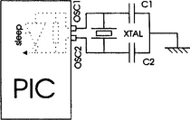
As mentioned, PIC microcontrollers will work with crystal oscillators, ceramic resonators or a simple RC circuit to produce these action-synchronizing clock pulses. Figure 3.4 shows the pinouts of various devices and a typical crystal oscillator application. The values of capacitors C1 and C2 depend on how the PIC derives its oscillator.
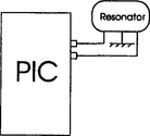
A minimal component count can be achieved by using a 3-pin ceramic resonator. These are available in frequencies from approximately 4 MHz to 8 MHz but with a reduced accuracy of only some 0.5% (compared with a typical accuracy of some 0.002% for a quartz crystal). The resonator would be used as in Figure 3.5. When using the programmer, a resonator can be selected by opting for the same XT mode as in a crystal.
Reset Circuit
When power is first applied to a microprocessor, it must be RESET so that the program can start from a known state. It will be RESET when the Master Clear (/MCLR) pin is connected to the 0 V supply. The PIC has internal circuits to perform this function at power-on and the simplest designs involve merely connecting the /MCLR pin directly to the +V supply or through a resistor to the +V supply. If, when the power supply is connected, the voltage rises too slowly, then this reset function may not work. In this case, Microchip recommend that the circuit of Figure 3.6 should be used. At switch-on, the capacitor is discharged. The PIC will be held reset until the voltage at /MCLR is above a threshold value. This will happen as the 100 nF capacitor is charged through the 470 W resistor.
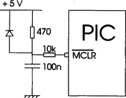
The PIC can be programmed to use an internal RC oscillator to generate a fixed 72 ms timeout on power-up. This is one of the options available when programming the IC. Other than that, there is also an Oscillator Start-up Timer which delays for 1024 oscillator cycles after the power-up delay. It ensures that the crystal or resonator has started and stabilized.
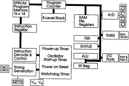
Internal Architecture
In the following descriptions and applications, the aim is primarily to explain the function of the 2C5xx or 16C5x PIC. Each instruction is a 12-bit word divided into an OPCODE which specifies the instruction type and one or more operands which further specify the operation of the instruction. (The more sophisticated members of the family use a 14-bit word.)
The 8-bit data bus connects two circuit components together:
• The register file composed of up to 80 addressable 8-bit registers. The first 8 of these are reserved for control or status reporting. The rest are general-purpose read/write registers. (Input/Output is ‘memory mapped’ which means that the I/O ports appear as an internal register. Inputting or Outputting data is as simple as reading or writing data to or from a memory location.)
The Arithmetic and Logic Unit (ALU)
The 8-bit wide ALU contains but one temporary working register (W register). It performs arithmetic and Boolean (logical) functions between data held in the W register and any file register. It also does single operand operations on either the W register or any file register.
Program Memory
Up to 512 words of 12-bit wide on-chip program memory can be directly addressed. Larger program memories can be addressed by selecting one of up to four available ‘pages’ with 512 words each.
Devices are available with either One Time Programmable (OTP) memory devices, or at greater expense, UV erasable memory devices. These are mostly used for development or pre-production models. Once the design is ‘mature’ then the OTP variants would be used.
Execution of the program instructions is controlled by the Program Counter (PC). At power-up or after a Master Clear, the PC is loaded with an address (1FFH for the PIC16C54). This is the address of the next instruction to be fetched. It is automatically incremented to point to the next valid address. Since the 16C54 can only hold 1FFH instructions, the PC automatically ‘rolls-over’ to 000. Jump (GOTO) instructions, Call instructions, Bit-Test-and-Skip instructions or computed addresses modify the contents of the PC. They are the only instructions which use 2 instruction cycles (8 clock pulses).
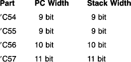
The stack itself is implemented differently from the 8051 (and most other microprocessors come to that). It is not part of the DATA or PROGRAM memory and the stack pointer cannot be manipulated (read to or written from) as in most other microcontrollers. The simpler PIC models have a limited STACK capability in that it is only two 12-bit addresses deep (12C5xx or 16C5x) or eight 14-bit addresses (16C6x, 16C7x, 16C8x). Care must be used to ensure that stack overflow or underflow does not occur by over-enthusiastic use of subroutines. This feature has sometimes been subjected to some criticism – mostly by engineers used to the tidy software discipline of multiple and nested subroutines. Consequently, PIC code tends to use a lot of macros.
The Stack
A stack is a device whereby an address can be saved for later reuse. It is most commonly seen when SUBROUTINES are CALLed. The sequence is:
1. The program code CALLs a subroutine.
2. The address of the instruction after the CALL is pushed onto the stack.
3. The program relocates to the subroutine by loading its address into the Program Counter.
4. When the subroutine has finished doing its business the RETURN instruction causes the address saved on the stack to be popped back into the PC.
5. Program execution continues where it left off before the CALL.
The Program Counter PC is a register which holds the address of the next instruction to be executed. The stack is usually referred to as a ‘first-in-last-out memory’, i.e. a RETURN statement will cause program flow to continue at the last address found on the stack.

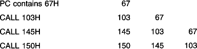
Initially, the PC contained 67H which means that the next instruction was located at that address. By executing CALL 103H, the address 67 is loaded onto the stack while 103 is loaded into the PC. This means that the next instruction to be executed would be at location 103H. At some point, the subroutine starting at 103H would contain the instruction RETURN. This reloads the address stored at the current top of STACK (67H) into the Programme Counter. Hence 67H is the address of the next instruction to be executed.
Problems occur if the CALL instruction is made too many times:
The situation is now that the original address can never be recovered no matter how many return instructions are issued. This is called stack overflow. If this becomes a limiting problem, the applications manual supplied with the PIC programmer gives a method of implementing a software stack.
12C5XX and 16C5x Register Structures
The registers can be divided into two categories:
Some of these registers use all of the byte or word to convey a particular value – such as the current count value in the Real Time Clock Counter (RTCC). Others rely on individual bits to control or monitor events – such as when bit 3 of the OPTION register controls whether the prescaler operates on the RTCC or Watchdog Timer WDT.
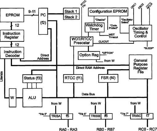
Operational Register Files
The lower 8 bytes of data memory are used for various register files (identified in Table 3.2 with an f-number) and as such have special functions to do with controlling or monitoring the microcontroller. They can all be read and written to by the software.
Table 3.2
| Address | Name | Function |
| 00 | f0 | Indirection Register |
| 01 | f1 | Real Time Clock/Counter Register |
| 02 | f2 | Program Counter |
| 03 | f3 | Status Word Register |
| 04 | f4 | File Select Register |
| 05 | f5 | Port A |
| 06 | f0 | Port B |
| 07 | f7 | Port C |
| 08–0F | f08–f0F | ’C54 ’C55 ’ C56 General-purpose Register Files |
| f10–f3F | ’C57 Bank 0 Register Files | |
| f30–f3F | ’C57 Bank 1 Register Files | |
| f50–f5F | ’C57 Bank 2 Register Files | |
| f70–f7F | ’C57 Bank 3 Register Files |
Special-purpose Registers
| W | Working Register |
| TRISA | I/O Control Register for Port A |
| TRISB | I/O Control Register for Port B |
| TRISC | I/O Control Register for Port C |
| OPTION | Prescalar/RTCC Option Register |
In more detail, the general and special registers are:
Address 00 (name f0).: Indirect register addressing. This is not a physically implemented register. Addressing f0 calls for the contents of f4, the File Select Register (FSR), to be used to select a file register. f0 is useful as an indirect address pointer. For example,
![]()
will add the contents of the register pointed to by f0 to the contents of the W register and place the result in W. (If f4 = 0, the implication is that f4 is pointing to f0 itself. In this case, 00 will be read.)
Address 01 (name fl).: Real Time Clock/Counter Register. This can be loaded and read by the program as any other register if required. In addition, its contents can be incremented by an external signal edge applied to the RTCC pin or by the internal instruction cycle clock. In this case, the instruction cycle clock is updated at a rate of (oscillator frequency)/4. An 8-bit prescalar can be assigned to the RTCC by writing the appropriate values to control bits in the OPTION register. So, if the PIC operates from an 8 MHz clock and the prescalar is set to 1:64 the RTCC register would be incremented every 32 μs.
Address 02 (name f2).: Program Counter. The program counter generates the addresses for up to 2048 × 12 on chip EPROM locations containing the program instruction words.
The program counter is reset to all 1s and is auto-incremented with each instruction unless the result of that instruction changes the PC itself. Hence the first instruction should be placed at 111111111B which is 1FFH, but many designers program a NOP (No-Operation) at this location so that the PC rolls over to the more conventional start of 000. When the 9-bit register contains 111111111, incrementing this by 1 causes the PC register to load with 000000000.
Address 03 (name f3).: Status Word Register. This contains the arithmetic status of the ALU and CPU. The individual bits are set or reset as a result of the preceding operation. For example, if the W register contains D0H (208D) and A0H (160D) is added to it, the result should be 170H (368D). The W register is only 8 bits wide (i.e. only capable of holding FFH (255D) as its largest number), so after the addition, the register would actually contain 70H (112D) and the C bit would be set.
If the W register contains 31 and 31 is subtracted from it, then as a result of this sum, the zero Z bit would be set.
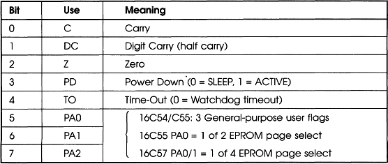
Nearly all programs rely on testing bits in the status register and jumping to one or other parts of the program depending on whether or not the bit is set. Table 3.3 shows the bits in the status register.
Table 3.3
Most software programmers create a header file with these in for ease of programming. For example, it is easier to remember the instruction:
![]()
than
![]()
The BSF mnemonic is the Bit Set in File instruction. In this case, bit 5 of file register 3 is being set. The bits and file register would be labelled with EQU commands such as
![]()
Address 04 (name f4).: File Select Register. If it is not used for indirect addressing, f4 can be used as a general-purpose register for holding any 8-bit data. As a File Select Register, bits 0–4 select one of the 32 file registers which will act as one of the instruction operands. This allows an amount of auto incrementing through the register files. In the 16C57, bits 5 and 6 additionally identify and select the current data memory bank. All the other bits are read as 1s.

Input/Output Operations
I/O control registers: The previous example showed how to output a value to a port. In this case, it was H’7E’ (B’01111110′). Before this can be done, the port must be set up so that the individual pins act either as an input or an output. The I/O control register is loaded with the content of the W register by executing the TRIS instruction. A ‘0’ puts the contents of file register f5, f6 or f7 onto the selected I/O pins. These registers are write only and are set to 1 on a RESET. In other words the default state of the I/O pins after a RESET is as inputs.
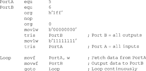
For example, to set all of the pins of port B as outputs (16C5x):
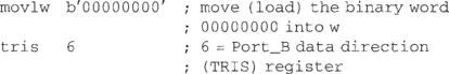
(Although for the more complex PIC devices, this procedure takes a few more steps to access the data direction register.)
Thereafter, a byte could be output with a command such as:
![]()
Of course, labels are more meaningful, so a program would be written more usefully as:

Lines 2, 3 and 4 are the result of the reset vector structure of the PIC family.
At a reset, the Program Counter (PC) is set to

This is the location of the RESET VECTOR and the first instruction of the program which will be executed after a RESET. In the 16C5× family, the RESET VECTOR is set at the top of memory, so the first instruction must be to relocate to another part of memory. This relocation is usually a GOTO 0 or NOP (no-operation) instruction.
The following example continually reads the lower four bits of Port A and copies them to Port B:
If Port A has been set to all inputs, then individual bits could be set or cleared using the BSF or BCF command:
![]()
Testing individual bits is achieved with the bit test and skip instructions BTFSC and BTFSS. The ‘skip’ means that the next instruction will be missed out if the bit tested is Clear (BTFSC) or Set (BTFSS).
Questions
1. Set up a 16C54 with RA0–3 as inputs and RB0–3 as outputs. Copy the inputs on the RA ports to the outputs on the RB ports.
2. Repeat question 1 but make RB0–3 the inputs and RB4–7 the outputs. When a ‘1’ appears on RB0, RB4 should follow. Similarly the pairs should link RB1 & RB5; RB2 & RB6; RB3 & RB7.
3. Write a program which sets Port B bits 0–3 as inputs and Port A bits 0–1 as outputs. Port A should show in binary how many of the inputs are HIGH.
Motor Control
A fairly trivial example of a 16C54 in use is as a latching push-button motor control. Figure 3.8 shows the circuit diagram of a conventional pair of ON-OFF push-buttons controlling a motor. For this example, the motor is mains operated, and so a relay is used to supply power. The inputs are a normally open contact pair for ON and a normally closed contact pair for OFF. This is the usual configuration for industrial controllers. Also note that there is no need to set up Port A since it is only used as an input port. This is the default condition for any port. Electrically, however, it is not wise to leave inputs ‘floating’. Electrical noise could couple into the PIC, or electrostatic charges could damage the chip. The solution is either to ‘pull-up’ the unused inputs to the positive voltage supply through (say) a 10 kW resistor or to program unused pins as outputs. The following code should suffice:

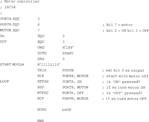
The only new instructions seen in this code example are the BTFSS/BTFSC Bit Test File and Skip instructions. These cause the program flow to Skip (the next instruction) if Bit Set and Skip (the next instruction) if Bit Clear. With the control buttons as shown:
If the push buttons are in the normal position, then the next instruction to turn the motor on or off is skipped.
Counter Timer Register
OPTION. This defines the prescalar assignment (RTTC or WDT), prescalar value, signal source and signal edge for the RTCC. The OPTION register is write only and is 6 bits wide. By executing the OPTION instruction, the contents of the W register will be transferred to the option register. At RESET, the option register is set to all 1s.
This means that default condition is to use the Watchdog Timer at a rate of 1:128. If the Real Time Clock Counter is selected (bit 3 = 1), the other bits in the OPTION register allow you to choose whether the internal clock is used or whether an external clock is used. If the internal clock is selected, (bit 5 = 0), then the RTCC register (f01) will be incremented at a rate determined by the system clock and the PS bits of the OPTION register. If external is selected, (bit 5 = 1), then the choice is between whether the RTCC register (f01) is incremented when this external clock goes Low (1–0 transition; use bit 4 = 1) or when it goes High (0–1 transition; use bit 4 = 0).
Table 3.4
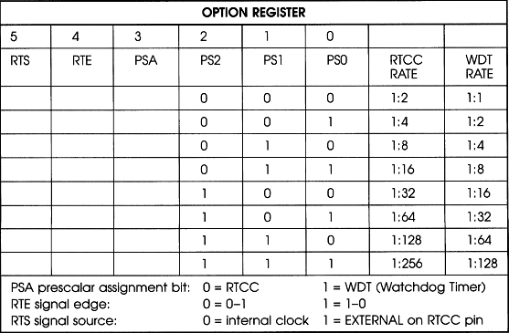
For example, to set a 1:64 rate on the RTCC internal clock:
![]()
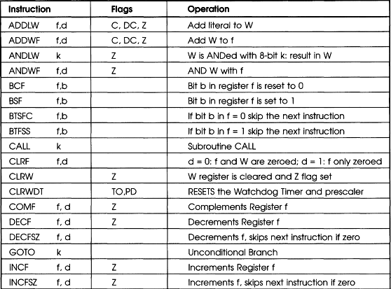
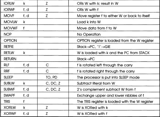
The 16C5x Instruction Set
| Notes | |
| f | file register |
| d | destination: 0 = W register, 1 = file register |
| b | bit field |
| k | 8- or 9-bit constant |
SLEEP mode: when in a low power SLEEP mode, the IC is woken up either by a master reset (register information will be lost) or by the Watchdog timing out. This is a useful mode of operation for battery powered equipment since it takes less current from the supply when in sleep mode. The oscillator driver is turned off although the output ports maintain the same values that they had before the SLEEP instruction was issued. Current drain can be reduced further by setting the outputs to act as inputs while the PIC is asleep (if this is electrically acceptable in the application circuit!). There is a simple program and further explanation on page 107.
Simple Programming Examples
The PIC family has only one register – the W or working register. The rest of the registers are part of the inbuilt file registers (RAM). Like all other microprocessors, a lot of the user programs are concerned with transferring data between registers with such commands as:
| ADDWF | Add working register to file register |
| ANDWF | AND working register with file register |
| IORWF | OR working register with file register |
| SUBWF | Subtract working register from file register |
| SWAPF | Swap upper and lower nibbles of file register |
| XORWF | Exclusive OR working register with file register |
Table 3.5
| Instruction | Flags | Operation |
| ADDWF f, d | C, DC, Z | Add W to f |
| ANDLW k | Z | W is ANDed with 8 bit k: result in W |
| ANDWF f, d | Z | AND W with f |
| BCF f, b | Bit b in register f is reset to 0 | |
| BSF f, b | Bit b in register f is set to 1 | |
| BTSFC f, b | If bit b in f = 0 skip the next instruction | |
| BTFSS f, b | If bit b in f = 1 skip the next instruction | |
| CALL k | Subroutine CALL | |
| CLRF f, d | d = 0: f and W are zeroed; d = 1: f only zeroed | |
| CLRW | Z | W register is cleared and Z flag set |
| CLRWDT | TO, PD | RESETS the Watchdog Timer and prescaler |
| COMF f, d | Z | Complements Register f |
| DECF f, d | Z | Decrements Register f |
| DECFSZ f, d | Decrements f, skips next instruction if zero | |
| GOTO k | Unconditional Branch | |
| INCF f, d | Z | Increments Register f |
| INCFSZ f, d | Z | Increments f, skips next instruction if zero |
| IORLW k | Z | ORs W with k; result in W |
| IORWF f, d | Z | ORs W with f |
| MOVF f, d | Z | Move register f to either W or back to itself |
| MOVLW k | Load k into W | |
| MOVWF f | Move data from f to W | |
| NOP | No Operation | |
| OPTION | OPTION register is loaded from the W register | |
| RETLW k | W is loaded with k and the PC from STACK | |
| RLF f, d | C | f is rotated left through the carry |
| RRF f, d | C | f is rotated right through the carry |
| SLEEP | TO, PD | The processor is put into SLEEP mode |
| SUBWF f, d | C, DC, Z | 2’s complement subtract W from f |
| SWAPF f, d | Exchange upper and lower nibbles of f | |
| TRIS f | The TRIS register is loaded with the W register | |
| XORLW k | Z | W is XORed with k |
| XORWF f, d | Z | W is XORed with f |
Each of these instructions has a destination register which is specified in the instruction itself. W and F are reserved constants (0 and 1 respectively) which inform the assembler of the destination register. For example:
![]()
In practice, of course, file register 12 would be given a more meaningful definition in the EQUATES section, perhaps something like
Then we could see a line such as
![]()
The MPSTART software is distributed with a file called PICREG.EQU, reproduced on page 111. This is a full listing of all the register and useful function names. It may be used as a header file for a program by means of an instruction such as:
![]()
The effect of this line is to act as though the code in the file named had been inserted at that point in the source code prior to assembly.
In a particular program, a file location has been EQUated to the word TEMP and that location is to be loaded with the binary number 10010110.
This could be done with the sequence:
![]()
or even:
![]()
if the constant value is equated to B′10010110′.
Like all other microprocessors, the PIC is capable of indirect addressing. It uses both register 0 and register 4. Reading or writing data to register 0 causes that data to be read or written to whichever register is held (pointed to) by register 4. For example:
![]()
would actually cause the data in location 13 H to be loaded into the W register. An advantage of using indirection is that sequential memory locations can be manipulated easily by incrementing or decrementing the contents of the F4 register.
Members of the PIC16C5x family
The full membership of the PIC16C5x family are
• 16C54. The base unit has already been described in the preceding pages.
• 16C55. A variant of the ‘C54 but is issued in a 28-pin Integrated Circuit (IC) and has an additional 8-bit I/O port called Port C. It has the same memory capacity, i.e.
• 16C56. An 18-pin IC with a 4-bit Port A and an 8-bit Port B (like the ‘C54). It is an expanded version with 1024 program memory locations and 32 data memory locations.
• 16C57. The same I/O capacity as the ‘C55 (4-bit Port A, 8-bit Port B, 8-bit Port C). It has much larger memory capacity in that it has 2048 program memory locations and 80 data memory locations.
I/O Port Structures
Electrical Characteristics of the I/O Pins
Figure 3.9 shows the typical internal schematic arrangement of the I/O pins. All of the ports can be used for both input and output activities. Prior to use, the programmer must set the data direction on each active I/O pin. Only if the I/O control latch has a ‘0’ written to it will the transistors Q1 or Q2 be able to be driven. This would happen if the programmer loads the W (working) register with a ‘0’ (O = output) for each pin to act as an output.
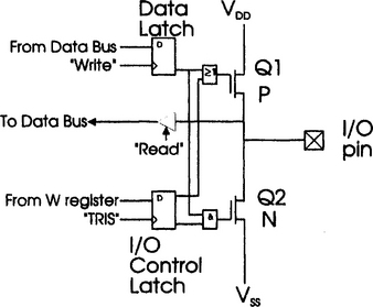
For example, writing the byte 00001111 to the TRIS (the PIC name for a Data Direction Register) would cause its upper nibble to be an output while its lower nibble would be an input.
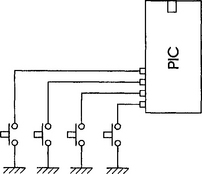
Any port (A, B or C) can source 40 mA total or sink 50 mA total. An individual I/O pin can source 20 mA and sink 25 mA. Thus pins could be used to directly drive output devices such as LEDs. However, the temptation to use this capability should be curbed when directly handling inductive or capacitive loads because of the risk of EMC problems. Most practical o/p devices should be driven with appropriate devices – be it via discrete components such as transistors or via integrated circuit device drivers – Figure 3.10 shows a few possible devices. The Bipolar Transistor Darlington pair has a current gain of a minimum of 1000, so, for example, a DC load which draws 5 A would only draw a maximum of 5 mA from the I/O port. The MOSFET is a voltage operated device and draws very little current (mA) into the gate. The driver array is an IC with a set of Bipolar Transistor Darlington pairs.

Omitted for simplicity are the freewheel (sometimes called back e.m.f.) diodes which are connected across the load with their cathodes to the positive supply. These protect the drive transistor against the very large e.m.f. which can be generated when turning off the current to an inductive load. Even with a 5 V supply, this reverse voltage could cause the collector (or drain) of the transistor to rise rapidly to 300 V or more. This is usually fatal for the transistor. The output driver IC has these diodes built in. The more sophisticated 16C64, 16C71, 16C74 and 16C84 offer the option of pull-up ‘resistors’ inside Port B so that input devices such as push-buttons, keypads etc. can be directly connected to the PIC with no additional passive components. These resistors are actually formed from transistors and are referred to in the manuals as ‘weak pull-ups’.
Timing
The PIC family all have a Real Time Clock Counter (RTCC) register (01). It can be read or written to just like any other register, but can also be incremented by either the system clock or an external signal (via the RTCC pin). The 16C5x family has no interrupt structure so the register must be regularly polled to see if the required time/count has elapsed. When the register reaches FF, it ‘rolls over’ to 00. Figure 3.12 shows the schematic arrangement of the RTCC. The bits RTE RTS PS2 PS1 AND PS0 are located in another control register called the OPTION register which is loaded from W by the OPTION command.

A 16C5x operating from a 4 MHz clock has an internal clock rate of 1 MHz (foSc/4). If the prescaler is set to 256, the RTCC register would be incremented every 256 μs. Thus the maximum time would be 256 × 255 μs or 39.68 ms.
Here is an example piece of code which is intended to produce a pulse train of 1 ms pulses with 1 ms spaces. If the prescalar is set to 4, the RTCC is updated every 4 μs. If the RTCC is preloaded with 06 then after 250 increments, the RTCC will be at 0 (testable in the status register).

Questions
1. Write a program for a 16C54 which outputs from pin RA1 a continuous stream of pulses ON for 1 ms and OFF for 5 ms.
2. A 12C508 has a push button connected to pin 7. When pressed, the output on pin 6 should produce 1 kHz tones for 0.2 s with 0.3 s between tone bursts.
3. A 12C508 has an input line on pin 2. Following a positive transition on this input, the output on pin 5 should go high for 1 s, followed by a 2 s pulse on pin 6 followed by a 4 s pulse on pin 7.
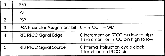
Table 3.7

The Rest of the Family
This is a more difficult task than with the 8051. The PIC families are constantly evolving and new versions are coming out all the time. Table 3.8 shows the essential differences.
Table 3.8
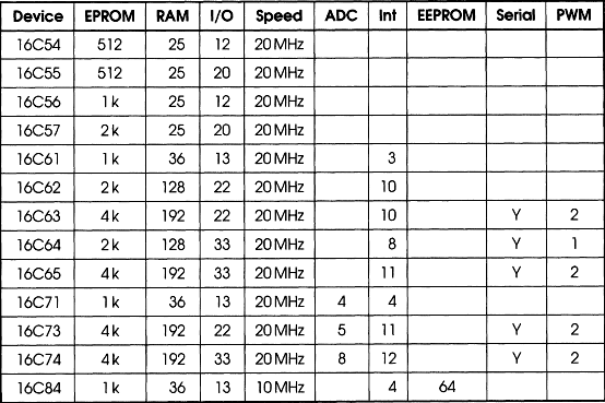
Many engineers start by considering the base members of the family – the 16C5x group – and after finding their limitations, move on to something more productive. In fact, technology has moved on so far from these base members, that they do appear to be extremely limited in what they can offer (except cost and simplicity, of course). The first real improvements came when Microchip started offering devices with interrupts and a better depth of stack. The drawback was that they then had to redesign the data memory map to accommodate all the extra facilities. The way that they did it was to create a direct memory map (Register Page 0) which was the default option and to have a second memory map (Register Page 1) which was accessed by setting one of the bits in the STATUS register (bit 5 – RP0). Most of the registers are merely duplicated, but some of them change function. The most common change is typically for the Register Page 0 registers to hold data, while the corresponding Register Page 1 registers hold the control/status information. This is the general idea, but some of the details vary from device to device, so care must be taken to study the data memory map carefully.
The following pages give some extra detail about the 16C71, 12C67x and 16C84.
PICs with ADC
The PIC16C71 of the PIC family has all of the attributes of the 16C5x with the following main differences:

The PIC12C671 and 672 are the 8 pin equivalent of the 16C71. Of the 6 I/O pins, up to 4 can be configured as ADC inputs. Once again, the main advantage is the compactness of the design.
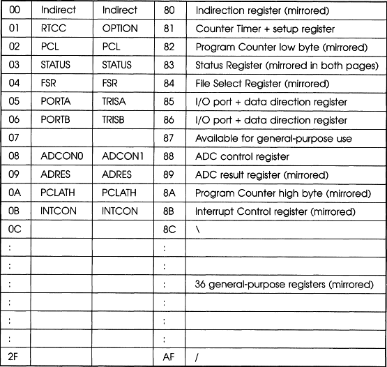
The data memory map now becomes as shown in Table 3.9.
Table 3.9
The STATUS register also changes some of its functions, see Table 3.10.
Table 3.10
| 0 | C | Carry |
| 1 | DC | Digit Carry (half carry) |
| 2 | Z | Zero |
| 3 | PD | Power Down: 0 = SLEEP, 1 = ACTIVE |
| 4 | TO | Time Out: 0 = Watchdog Timeout |
| 5 | RP0 | Register Page 0: 0 = page 0 (00–7F), 1 = page 1 (80–FF) |
| 6 | RP1 | Register Page 1 (not currently implemented) |
| 7 | IRP | Indirect Register Page: 0 = page 0 or 1, 1 = page 2 or 3 (not currently implemented). The aim of this control would be to indirectly access a different register page |
OPTION Register
This has extra functions, as shown in Table 3.11.
Table 3.11
| 7 | 6 | 5 | 4 | 3 | 2 | 1 | 0 | ||
| /RPBU | INTEDG | RTS | RTE | PSA | PS2 | PS1 | PS0 | RTCC | WDT |
| 0 | 0 | 0 | 1:2 | 1:1 | |||||
| 0 | 0 | 1 | 1:4 | 1:2 | |||||
| 0 | 1 | 0 | 1:8 | 1:4 | |||||
| 0 | 1 | 1 | 1:16 | 1:8 | |||||
| 1 | 0 | 0 | 1:32 | 1:16 | |||||
| 1 | 0 | 1 | 1:64 | 1:32 | |||||
| 1 | 1 | 0 | 1:128 | 1:64 | |||||
| 1 | 1 | 1 | 1:256 | 1:128 |
| PSA | Prescalar assignment bit |
| RTE | RTCC signal edge |
| RTS | RTCC signal source |
| INTEDG | INTerrupt edge select |
| 0 | = RTCC |
| 0 | = L → H |
| 0 | = internal |
| 0 | = interrupt on failing edge |
| 1 | = WDT |
| 1 | = H → L |
| 1 | = transition on RA4/RTCC pin |
| 1 | = interrupt on rising edge |
Analogue to Digital Converter Programming
One of the main attractions of the 16C71 is the use of Port A as 4 × 8-bit analogue inputs with a typical 20 μs conversion time per channel. One of these four inputs can be selected via an internal sample and hold circuit and the 8-bit result of the conversion is left in register 09 – ‘ADRES’. Setup and control of the ADCs is via the ADC control registers ADCON0 and ADCON1.
A similar difference exists in the 16C67x 8 pin DIL except that there is only one GPIO (General Purpose Input Output) port. Up to 4 pins of these ICs can be configured as ADC inputs. Like the 16C71, there is actually only one Analogue to Digital Converter. Software selects which of the inputs is routed to the ADC.
Port A is register 05 and its corresponding direction control register TRISA is mapped in page 1 of register file at address 85 H. Port A is a 5-bit wide port with pins RA0–RA4. Port pins RA0–RA3 are bidirectional whereas RA4 has an open collector output. Pins RA0–RA3 also have the alternate function AIN0–A1N3. The standard voltage reference for these pins is the supply voltage, although RA3 could further be used to input an external voltage reference (of NOT greater than the supply voltage). The A/D converter will thus provide a byte of information (0–255) which corresponds to a proportion of the supply voltage or whatever voltage is applied to pin RA3.
The two control registers ADCON0 (address 08h) and ADCON1 (address 88h) are used as shown in Table 3.13.
Table 3.13
| ADCON0_7 | ADSC1 | ADC clock select |
| ADCON0_6 | ADSC0 | ADC clock select |
| ADCON0_5 | General-purpose read/write bit | |
| ADCON0_4 | CHS1 | Analogue channel select: 00 AIN0, 01 AIN1 |
| ADCON0_3 | CHS0 | Analogue channel select: 10 AIN2, 11 AIN3 |
| ADCON0_2 | GO/!DONE | Set to 1 to begin conversion, reset to 0 by hardware to indicate conversion is done |
| ADCON0_1 | ADIF | A/D conversion complete interrupt flag bit. Set when conversion is completed. Reset in software |
| ADCON0_0 | ADON | 0 = A/D converter module is shut off and consumes no operating current |
The ADC clock can be derived from the system clock or from an internal RC oscillator. The period of the RC oscillator varies, but is typically 4 μs–2 μs. Being a successive approximation conversion device, it takes 10 ADC clock periods to complete the conversion.
Bits 4 and 3 of ADCON0 are used to select which of the inputs of Port A are to be selected for conversion:
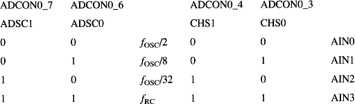
ADCON1 uses only two bits, which configure the function of pins RAO–RA3:

The 16C71 has 4 inputs which can be routed to a sample and hold circuit which is connected to an 8-bit successive approximation analogue to digital converter. The inputs are connected to Port A bits 0, 1, 2 and 3. If not used for ADC purposes, then any or all of these bits can be used as conventional digital I/O. Port A bit 3 can additionally be used to input a reference voltage other than the default value of 0 V. To provide all these various functions, additional control registers are required. These are:
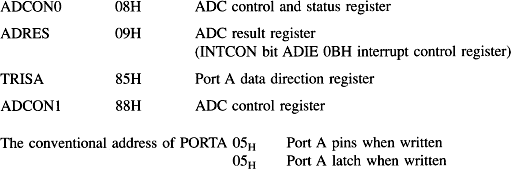
A peculiarity of the 16C71 is that register files (RAM) exist in four blocks of 128 bytes. The blocks or pages are identified/set up by two bits (RP0 and RP1) in the status register (03). ADCON1 is mapped in PAGE 1. This means that in order to write to it you must SET bit 5 of the STATUS register (reviewed overleaf).
The following code is a continuous conversion of Channel 2:

The Port B data direction register is 86H in this device instead of 06H as in the 16C5x family. However, when selecting Page 1, the actual address becomes 06 – the result of having an addressing range of 127 bytes. Trying to write to 86H will result in an assembler warning (when using the mpasm assembler).
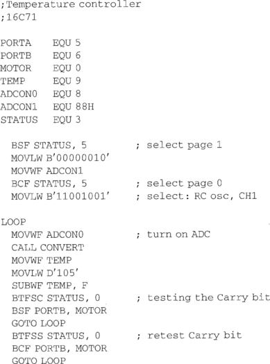
The conversion must be to some purpose, so the following example is a simplistic temperature controller as in Figure 3.15. A temperature sensor is connected to AIN1.
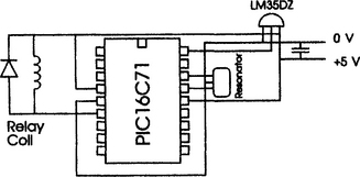
If the temperature is below a digital value of 105, the heater (Port B bit 0) is turned on, while when the temperature rises above this level, the heater is turned off.

Status Register (03)
Several references have been made to the Status Register. This is readable and writeable and hold the results of the previous operation.
0. Carry/Borrow (C). Set if there is a carry in or out during add or subtract operations. It also holds the overflow bit during rotate operations.
1. Digit Carry/Borrow (DC). Used during BCD arithmetic and is set if there is a carry out from the 4th low order bit of the resultant.
2. Zero bit (Z). Set if the result of an arithmetic or logic operation is zero.
3. Power Down bit (PD). Set during power up or by a CLRWDT command. Reset by the SLEEP command.
4. Timer Out bit (TO). Set during power up and by the CLRWDT and SLEEP command. Reset by a watchdog timer timeout.
| PA1 | PA0 | |
| 0 | 0 | Page 0000–1FF |
| 0 | 1 | Page 1200–3FF |
| 1 | 0 | Page 2400–5FF |
| 1 | 1 | Page 3600–7FF |
Interrupts on the PIC
The PIC 16C71 supports one of four interrupt sources:
| External | External INT pin RB0. This is an edge sensitive input and can be set to trigger an interrupt on rising transitions of RB0 or falling transitions of RB0. The appropriate edge is set in the OPTION register. |
| Timer | Counter/Timer. When the RTCC Counter Timer0 register overflows from a count of 255 to a count of 0. |
| ADC | End of analogue to digital conversion. |
| Change | If one of RB7–RB4 changes state, then an interrupt can be triggered. |
To assist this, there is a new register, the INTerrupt CONtrol register (INTCON) which is located at address 0BH. All pins of INTCON are readable and writeable: there are 5 controls which enable or disable interrupts and 3 flags which indicate when an interrupt has occurred. (The fourth flag, for ADC end of conversion, is located not in INTCON, but in ADCON0-bit 1.)
After a RESET (Master Clear) the GIE bit is cleared, so all interrupts are inhibited. If you wish to use interrupts in a program, this bit must be set along with the Enable bit of the interrupting source you want to use.
Table 3.14
| INTCON7 | GIE | Global Interrupt Enable. This is the master control which can be used to disable all interrupts: 0 = Disable all interrupts, 1 = Enable |
| INTCON6 | ADIE | A/D conversion Interrupt Enable: 0 = Disable A/D interrupt, 1 = Enable A/D interrupt |
| INTCON5 | T0IE | Timer TMR0 interrupt enable bit: 0 = Disable TMR0 interrupt, 1 = Enable TMR0 interrupt |
| INTCON4 | INTE | INT interrupt enable bit: 0 = Disable INT interrupt, 1 = Enable INT interrupt |
| INTCON3 | RBIE | RBIF interrupt enable bit: 0 = Disable RB change interrupt, 1 = Enable RB interrupt |
| INTCON2 | TMR0 | TMR0 overflow interrupt flag: 1 = RTCC overflow; reset by software |
| INTCON1 | INT | INTerrupt flag: 1 = INTerrupt occurs; reset by software |
| INTCON0 | RBIF | RB Port B change interrupt flag: 1 = one of Port B bits 7–4 changed; reset by software |
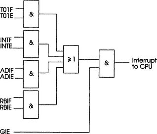
Once in the interrupt service routine, the source(s) of the interrupt can be determined by polling the interrupt flag bits (see software examples). The interrupt flag bit(s) must be cleared in software before re-enabling interrupts to avoid more interrupts. RETFIE, the return from interrupt instruction, exits the interrupt routine as well as sets the GIE bit to re-enable interrupts. (An alternative instruction ‘RETURN’ returns program control to the point at which the interrupt was invoked but does not re-enable interrupts.)
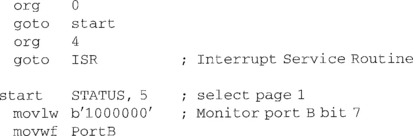
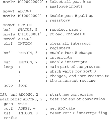
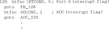
The following code sets up an interrupt and carries out an ADC conversion on channel 0 whenever the push-button connected to Port B pin 7 is pressed. For simplicity, some of the EQUates at the header of the program have been omitted.
This is a fairly simplistic program, kept simple by allowing only one type of interrupt – the Port B change interrupt. It would be perfectly possible to use interrupts triggered by the End of Conversion flag. In this case, there would have to be code at the start of the ISR to determine which routine caused the interrupt. Something along the lines of:
Questions
1. Write a program for a 16C71 which reads the analogue voltages on AD0 and AD1 and outputs the largest as a binary number on port B.
2. Write a program for a 16C71 which reads the analogue voltages on AD0, AD1 and AD2. If the values of AD1 falls between that of AD0 and AD2, make PB0 ‘1’, otherwise make PB0 ‘0’. This circuit function is also called a Window Detector.
3. Write a program which continuously reads the voltage on AD0. Output its largest value on Port B. If AD3 is ‘1’ rather than ‘0’, reset the value of Port B to the current vale input on AD0. This circuit function is called a Peak Detector.
4. Continuously sample the analogue voltage on AD0. When the value decreases, pin PB0 should pulse high for 1 ms.
Figure 3.17 shows one possible implementation of a push button operated a.c. power controller. The opto triac/triac combination is explained on page 117.
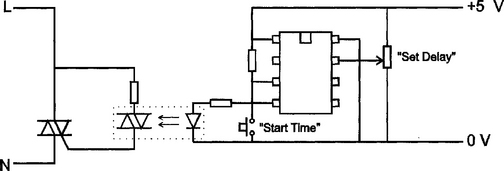
Figure 3.17
Stack
The device supports an 8-level stack. This is better than in the 16C5x family, but care must still be taken not to overflow this facility.
PIC16C84 with EEPROM Management
The main feature of this 16C5x-like device is that it uses EEPROM memory for both program and data. The program memory cannot be programmed ‘in-circuit’ or ‘interactively’, but it does provide a cheaper option than the EPROM version. When programmed with the MPSTART or other programmer, the contents of program memory will be erased before the new program is committed to EPROM. Many engineers use this IC as their main development tool prior to installation in OTP form – especially if they haven’t yet committed themselves to an In Circuit Emulator – that essential workhorse of the professional developer.
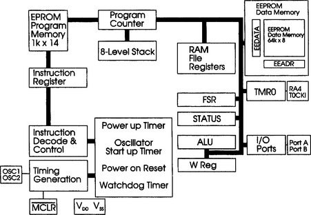
There are 36 data registers and an additional 64 × 8-bit EEPROM data memory locations. This means that essential data memory can be saved even though power is removed from the device. Figure 3.18 shows the internal structure of the PIC16C84.
It has the same 8-level stack and 4 interrupt sources as the 16C71, although the ADC interrupt is replaced by one related to the use of the EEPROM data memory structure.
The data register memory map for this device is shown in Tables 3.15 and 3.16.
Table 3.15

Option Register
This has a specific memory location in register page 1 (81).
Table 3.17

Status and Option registers have more or less the same function as in the 16C71, but the INTerrupt CONtrol register INTCON has slightly different functions to reflect the fact that the 16C84 has an EEPROM data memory rather than an ADC capability.
To implement the input push buttons as suggested in Figure 3.11, a ‘1’ would have to be written to bit 7 of the OPTION register (81).
The INTCON register is defined as in Table 3.18
Table 3.18

Data EEPROM Management:
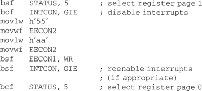
The 64 × 8 EEPROM data memory is accessed through two registers EEDATA (address 08) and EEADR (address 09). EEADR only has a valid range of 00–63. The storage and retrieval of data is controlled by the two registers EECON1 (address 88) and EECON2 (address 89) although EECON2 is not currently implemented. While it has a high number of write/erase cycles (1 000 000 typically), the write process is fairly lengthy, taking as it does 10 ms. Reading takes a conventional 1 clock cycle. EECON1 is as shown in Table 3.19.
Table 3.19

There is a somewhat unusual sequence to follow to write data to the EEPROM. First, the WREN WRite ENable bit must be set, and then for each byte, the address and data is written to the EEADR and EEDATA registers respectively. Then there must be the sequence of:
All interrupts must be disabled during this sequence.
Before the next byte can be written, the WR bit must be tested to see if the hardware has cleared it, or alternatively, an EEPROM interrupt handler can be used.
Reading the EEPROM data memory is somewhat more conventional. The programmer must:
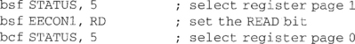
The data will then be available in the EEDATA register on the next cycle. It remains in EEDATA until that register is overwritten by another EEPROM READ or WRITE action.
The Watchdog Timer
The watchdog timer uses an internal free-running RC oscillator which is either enabled or disabled as part of the programming procedure. Once the device has been programmed, it is not possible to ‘turn off’ an enabled watchdog, nor is it possible to ‘turn on’ a disabled watchdog. The watchdog will RESET the processor if the instruction CLRWDT is not regularly issued.
Like the RTCC, the WDT prescalar bits are set via the OPTION command/register to alter the nominal timeout period of 18 ms. The timeout periods vary with temperature, VDD and process variations from part to part. The three bits PS2, PS1 and PS0 in the OPTION register determine the WDT rate prescalar (Table 3.20):
Table 3.20
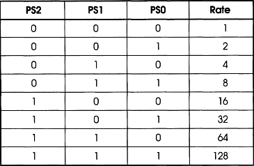
The longest time period is when the three bits are set to 111. This represents a sleep period of some 128 × 18 ms = 2.304 seconds. The following trivial example sends the PIC to sleep and allows it to reawaken after a timeout of 64 × 18 ms = 1.15 s. Upon reawakening, this trivial example merely increments the value output from Port B. Putting the PIC to SLEEP is a useful technique as it reduces power consumption to <3 μA (16C54).

Power Down Mode
The power down mode is entered by executing a SLEEP instruction. If enabled, the watchdog timer will be cleared but keeps running, the Power Down bit ‘PD’ in the status register (03) is cleared, the Time Out ‘TO’ bit is set and the oscillator driver is turned off. The I/O ports maintain the status they had before the SLEEP command was executed. This mode is used to draw minimal current, and it can be reduced further by all I/O pins at either VDD or VSS with no external circuitry drawing current from the I/O pin.
The device can be awakened by a watchdog timer timeout (if it is enabled) or an externally applied ‘low’ pulse on the RESET (Master Clear MCLR) pin. The PIC will stay in the RESET mode for one oscillator start-up timer period before normal program execution occurs. As explained previously, the ‘PD’ and ‘TO’ bits in the STATUS register indicate the cause of the system wake-up/reset.
| TO | PD | |
| 1 | 1 | Power Up |
| 0 | X | Watchdog Timeout |
| 1 | 0 | SLEEP instruction |
| 1 | 1 | Clear Watchdog CLRWDT instruction |
If the code uses the Watchdog and/or SLEEP facility, then it is important that the first few instructions establish the cause of the RESET. If the facilities are not used, then no such check would be needed.
If the PIC is awakened from a SLEEP by a WDT timeout then processing continues at the instruction following the SLEEP command.
The Prescalar can act on either the WDT or the Timer, but not both simultaneously. It may be necessary to reassign the Prescalar from one to the other under program control. This is fine, but it is essential to avoid a Timer or WDT timeout in the middle of the process. The way to avoid this is to issue a CLRWDT or CLRF TMR0 before reassigning that Prescalar.
Subroutines vs Macros
Subroutines operate in the PIC in the same manner as any other processor. The address of the Program Counter (PC) is pushed onto the stack and then the address of the subroutine is loaded into the PC. The routine re-enters the main routine by popping the return PC address off the stack and into the PC. Some of the code presented has already used subroutines.
The subroutines are usually kept together at the end of the program immediately before the end statement. They can be invoked with the instruction CALL, e.g. CALL CONVERT. They are identified by a label (in this case the subroutine is called CONVERT) and are terminated with some form of RETURN statement. This returns the program counter to the instruction after the CALL instruction. There are three versions of the RETURN instruction:
RETURN Return to the instruction which follows the CALL instruction
RETLW k As above, but load the W register with the number k first
The difficulty with subroutines is that they need a large stack capability to work effectively. Since most PIC models have a stack of depth 2 or 8, it can be a serious limitation to the programmer. It is the programmer’s responsibility to ensure that subroutines are not nested too deeply. The effect of doing so has already been demonstrated – the return address is eventually lost, and the program would in all probability crash.
Macros
A macro is a piece of code which is caused to be inserted into the program whenever its name appears. It enables effective software reuse, and yet does not depend on the stack. A macro is written and included at the start of the program. Like the subroutine, it is given a label. When it is invoked (not by calling, but by just using the label name) the source code is assembled into the code at that point. This is one of its main disadvantages. If a subroutine is called on five occasions, there will just be five call statements relocating the program to the one instance of that subroutine. If a macro is invoked five times, all of the macro code will be assembled into machine code five times.
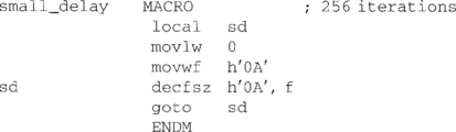
The macro is called small_delay and uses one local label sd. It loads the W register with 0 and decrements it until it reaches 0 once more. It uses register 0A to hold intermediate results. It is a very crude delay macro. In use, one might invoke the macro with a statement such as small_delay. At that point in the program all of the assembly language for the code would be included.
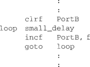
The following code has a similar action to the previous example of the SLEEP program. The value of Port B is incremented continuously. Well named MACROs make the code easier to read.
The reason that macros are so useful and powerful is the fact that they can take parameters:
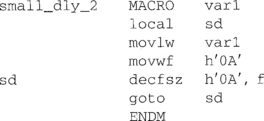
In this version, the macro can be invoked with a supplied parameter, e.g. small_dly_25 5. This would cause a delay count of 55 to be implemented, while small_dly_28 7 would cause the delay to be 87 counts. In the first case, the variable var1 takes the value of 55, so when the line
![]()
is implemented, the assembler replaces the text ‘var1’ and replaces it with 55. The effect is to load the working register with 55. i.e. as if the line had been
![]()
The advantage is of course, that the value loaded into W can alter each time that small_dly is called. The number of macro parameters which can be handled is limited by the software assembler. They must have unique names such as var1, var2, var3 etc. and are usually separated with commas. Check with your documentation, but it is not uncommon for an upper limit of 32 parameters to be available. This is certainly more than the average programmer would ever want or dream of! The parameter need not just be number. On assembly, a simple text replacement process is worked through, so the parameter could be a label or register name. Some programmers have used the facility to extend the basic instruction set to the extent that it resembles a high level language rather than assembly language.
Questions
1. Write a MACRO to swap the contents of any two register files which are the specified parameters. e.g., the code
![]()
would cause registers 0A and 0B to have their contents swapped, while
![]()
would cause registers 0C and 0D to have their Contents swapped.
The definition of the MACRO would start
![]()
2. Write a MACRO whose 1st line is
![]()
which takes a parameter var1 of value 0, 1, 2 or 3 which results in the W register containing the data from the specified port.
3. Write a MACRO for a 16C84 which stores the contents of the W register in the EEPROM location specified by the passed parameter.