RS232 and Other Serial Standards
RS232
This is a standard which defines serial transfer of data from one point to another. The interface is intended for short cables of up to 15 m between the two devices and at data rates from 50 to 76800 baud (bits per second). It is a flexible, user customizable standard, and its inherent flexiblity is one of the causes of people’s fear and mistrust of it. However, don’t dispair. With a basic understanding of the alternatives and common configurations, it is relatively easy to quickly set up a working communications link.
• It is also known as CCITT V24 standard.
• The standard is divided in four parts:
![]() definition of the plug, socket and pin assignment
definition of the plug, socket and pin assignment
![]() electrical signal characteristics
electrical signal characteristics
![]() functional description of the signals
functional description of the signals
![]() list of standard subsets of the interface signals for specific applications.
list of standard subsets of the interface signals for specific applications.
• RS232 divides the types of transmitter/receivers into either
This reflects the origins of RS232 from a teletypewriter system. Nowadays the terms usually refer to a computer system as DTE and a modem (for example) as DCE.
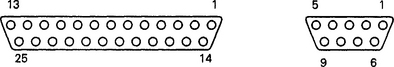
RS232 Connector Details
The connector system defined in the standard is the 25-way D-type connector, although there is also a 9-pin version which takes advantage of the fact that usually not all 25 pins are used. In fact, most RS232 applications use only nine of the pins and, if necessary, you can get away with using just three.
The pinouts are shown in Figure 5.1 and the pin function is described in Table 5.1.
Table 5.1

The asterisks show the signals which must be present for bidirectional data transfer. I have seen unidirectional data transfer systems which conform to a cut-down variant of RS232 with only 2 wires – TD or RD and SG.
Signal Details
FG Frame Ground is often left unconnected. It is connected to the chassis or metal frame of the equipments. It links the two cases and ensures that there are no dangerous voltages on the equipment cases. It provides an element of protection against faulty equipment and can also have a noise-reducing effect.
SG All of the RS232 signals are referenced to this ground. It is the one essential connection in the interface.
Interface Cable Varieties
In the conventional computer to modem link (DTE–DCE) the connection is just made point to point:
However, if the user wants to cut down on the number of lines, then each piece of equipment must be fooled into thinking that the other is in place and ready to go. (The obvious problem is that if for some reason one of the pair is not in place. Not to worry, this can be handled with software handshaking – more later.) When the DTE issues a Request to Send, it expects to get a Clear to Send signal. So, the obvious way to do this is to loop back the RTS into the CTS pin. Figure 5.3 shows the loopback present on both RTS/CTS and DTR/DSR.

Quite often, a designer may wish to use the RS232 protocol to interconnect two DTE equipments, such as two computers or microprocessors. In this case, null modem or crossover connections must be used, as shown in Figure 5.4.

Electrical Signal Characteristics
The RS232 standard uses negative logic and bipolar power supplies, i.e. a logic ‘0’ lies between +3 and +25 volts, while a logic ‘1’ lies between −3 and −25 volts. Figure 5.5 shows the voltage levels as the letter ‘Q’ is transmitted. ‘Q’ has the ASCII value of 51H and RS232 specifies that bits are transmitted Least Significant Bit first. So,
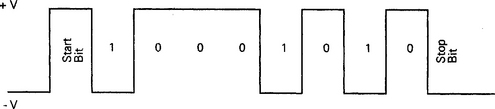
51H = 01010001B – transmitted as 10001010
Figure 5.5 shows clearly the rest state of the line as a ‘mark’ or ‘1’. The transmitted byte is framed with a Start and a Stop bit; Start being a logic ‘0’ and Stop being logic ‘1’. (Actually the Stop bit can be of length 1, 1.5 or 2 bit lengths long – as long as the sender and receiver agree beforehand which protocol is to be used, then all is well.)
The next pitfall for RS232 users is that the standard allows for data to be transmitted as 5, 6, 7 or 8 bits, with or without odd or even parity and at a variety of baud rates. This is explained as follows.
Parity is a very simple method of error detection. If parity is enabled, it is declared to be ODD or EVEN and consists of an extra bit between the data bits and the stop bit. If the transmitter and receiver agree to use ODD parity, then the total number of data plus parity bits must add up to an odd number. If EVEN parity is decided upon, then the total number of data plus parity bits must add up to an EVEN number. If NO PARITY is opted for, then the parity bit is omitted, for example:
• ‘J’ transmitted in 7-bit even parity would be 10010010
• ‘J’ transmitted in 7-bit odd parity would be 10010011
(‘J’ = 49H = 1001001 in 7-bit binary transmitted LSB first. ‘K’ = 4AH = 1001010 in 7-bit binary transmitted LSB first.)
The baud rate is simply the number of bits per second. Typically, these could be 75, 150, 300, 600, 1200, 2400, 4800, 9600, 19200 etc. This is not the rate at which data is transmitted, however. A 300 baud 8-bit system still requires the start and stop bits, so for each byte of data, 10 bits have to be transmitted. Hence the data rate would be 30 (300/(1 + 8 + 1)) bytes per second.
The rate should also be agreed before transmission commences. However, some equipment is auto-sensing in that it will try to sort out from the first characters transmitted the rate, parity and data size. It helps (or in some cases is essential) if the receiver knows what character to expect first. The space (20H) is commonly used for this purpose.
All these variables – connection, DTE/DCE, rate, parity, word size – give lots of factors which can stop one device from transmitting to or receiving from another. Despite this, RS232 is still probably the most commonly used serial protocol in the world.
Even the simplest of the 8031 family has an inbuilt capability to handle Serial RS232 data. Example code for the family was shown on page 47 in Chapter 2.
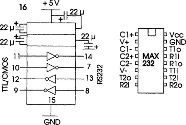
Voltage Level Conversion
One of the difficulties of RS232 from a hardware designer’s point of view used to be the awkward voltages used to characterize a ‘0’ and ‘1’. Fortunately, this is eased by families of ICs which operate from a single +5 V power supply and yet convert the 0/+5 logic signal to and from an RS232 voltage level. Internally these devices have two power supply sections:
One of the first companies to exploit this technology was MAXIM, and Figure 5.6 shows two typical applications using RS232 voltage converters.
Both 8051 and PIC microprocessor families have members which will output RS232 directly, but there are occasions when it is necessary to use the pins of a parallel input/output port. Before deciding to embark on this route, it is as well to consider what tradeoffs you are going to have to live with. In the first place, it is perfectly possible to design a pin output full duplex RS232 interface on a non-interrupt low capability microcontroller. However, it does take up a lot of memory space. Assuming that the IC is going to do something else useful as well as RS232, then it is as well to set some limits.
Full Duplex.: Do you really need it? The difficulty is that in a micro like the PIC16C5x family which only has but one timer, if you are transmitting a byte, and an incoming byte is detected on the input pin, then the RTCC timer has to cope with timing the outgoing byte at the same time as, and asynchronously with, the incoming byte.
Hardware handshaking.: Can it be avoided? This is less of a software overhead to manage and most devices these days can handle serial data at a considerable rate.
If all of this seems to be advocating some ‘shaky’ programming practices, then by all means use the more sophisticated devices (or in the case of the 8051, the inbuilt RS232 communication port).
RS232 involves the use of parallel to serial and serial to parallel converters. In software terms, the accepted technique is:
| output | input (when input detected) |
| load the byte into a register | wait one half bit period |
| (if required, calculate the parity) | read start bit status |
| transmit start bit | repeat |
| repeat | read bit into LSB |
| wait one bit period | shift all bits left circularly |
| output the LSB | wait one bit period |
| shift all bits right circularly | until all data bits received |
| until all bits sent | store byte into a register |
| (send parity if required) | (if required, calculate bit period) |
| (wait one bit period) | (read and compare parity bit) |
| transmit stop bit | wait one bit period |
| wait one bit period | read stop bit |
Of course, the clever part in this sort of programming is not in the successful, normal situation, but in the handling of errors. What happens if the parity does not match? What happens if the received start and stop bits are not as expected? So much depends on what sort of device is being transmitted to or from the microcontroller that there are many many answers to this sort of problem. Bulletin boards and web sites carry many examples of this type of software and it would be inappropriate merely to copy their sterling efforts in this book.
RS422 Transmission Standard
This serial standard has the virtues of faster data rate (up to 10 Mbits/s) and longer transmission distances (>60 m). It features a balanced double-ended transmission with driver output level in the range of ±2 V to ±6 V. Figure 5.7 shows the nature of the differential output, while Figure 5.8 shows a MAXIM application circuit with the MAX489 receiver/transmitter pair. The highest transmission rate is achieved by having separate pairs of data transmission lines – one set for data in and one set for data out.


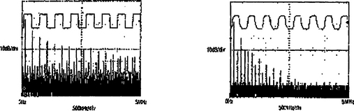
At the highest data rates, a lot of EMI (Electromagnetic Interference) would be generated because of the very fast edges of the square-wave output. To reduce the generated noise, some driver ICs use a trapezoidal output. This just means that the edges of the output waveform slope in a controlled way (‘slew-rate-limited’) to reduce the amount of electrical interference which is produced. Environmentally, and in terms of reliability, this is a good thing, but it does slightly reduce the maximum data rate. Figure 5.9 shows the output waveforms and frequency spectrum of non-slew-rate and slew-rate-limited signals.
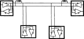
RS485 Transmission Standard
This standard is closely related to RS422 except that it is meant for multi-drop applications instead of point-to-point connections. Figure 5.10 shows a typical application.
I2C Configuration
The I2C or Inter Integrated Circuit bus was originally developed by Philips/Signetics. It is a simple two-wire interface. The main advantage of the bus is that it is economical with one of the microcontroller’s most precious resources – I/O capability. The number of devices which the two lines can connect is limited only by the total line capacitance not exceeding 400 pF. Each of these devices has a unique 7- or 10-bit address and can act as a master or a slave. The full protocol allows for multi-master, multi-slave devices with full collision detection and arbitration for when two masters try to transmit simultaneously. However, many designers keep life simple by using the bus in a single-master (microcontroller) multi-slave configuration.
Transfer of 8-bit data can be accomplished in one of two modes: standard (100 kbits/s) and fast (400 kbits/s).
The protocol offers the following definitions of I2C bus terminology:
| Transmitter | The device which sends the data to the bus |
| Receiver | The device which receives the data from the bus |
| Master | The device which initiates a transfer, generates clock signals and terminates a transfer |
| Slave | The device addressed by a master |
| Multi-master | More than one master can attempt to control the bus at the same time without corrupting a message |
| Arbitration | A procedure to ensure that if more than one master simultaneously tries to control the bus, only one is allowed to do so and the message is not corrupted |
The range of devices with in-built I2C bus is quite comprehensive, and includes: EEPROM, RAM, clock/calendars, LCD display drivers, 4-digit LED display drivers, gate arrays, ADC, DAC, keyboard interfaces, video/audio/radio processors.
Electrical Signals
The devices connect to the bus with open collector (or drain) transistors in the output stage of the integrated circuit and so each of the two wires of the bus must have a pull up resistor in the range of 1−10 kΩ, 4.7 kΩ being typical. Schematically, the bus looks like that shown in Figure 5.11.

Master/Slave Relationships
In Figure 5.11 SDA is the Serial Data line and SCL is the Serial Clock line. SCL is always generated by the masters when they try to initiate a data transfer. The data travels along the bidirectional line SDA. If Master 1 and Master 2 try to move data along SDA at the same time, the first one to output a ‘0’ when the other outputs a ‘1’ loses its access rights and has to wait until the other has finished.
At rest (no signal), both SDA and SCL are at logic ‘1’ (+5 V). Normally, SDA can only change when SCL is low – except that
• SCL at ‘1’; SDA ‘1’ to ‘0’ transition is the START TRANSFER condition
• SCL at ‘1’; SDA ‘0’ to ‘1’ transition is the STOP TRANSFER condition
Data is transferred in 8-bit bytes, MSB first. This will take 8 clock pulses, and an acknowledge is sent on the ninth clock pulse. Figure 5.12 shows a simple transfer of the binary word 11001001. The acknowledge is obligatory and indicates to the sending device that the receiving device recognizes and accepts the byte. The acknowledging device pulls the SDA line low to acknowledge.
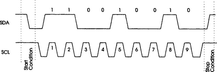
The first byte sent by the master is an address byte. As mentioned, each device has a minimum of a 7-bit address. For each device type, the first four bits are usually fixed, while the lower three are hardwired on the IC to provide a user programmable address. The eighth bit of the transfer is a read/write control. If bit 8 is ‘0’ then the master is WRITING. If bit 8 is ‘1’ then the master is requesting or READING data. Figure 5.13 shows some of the possible combination of transfers.

MCS51 Control Signals
Many of the 8051 family members can transmit and receive I2C signals. It is of course perfectly possible to program a standard member of the family to output bit by bit signals to other I2C devices. This does seem to be the last resort in a microprocessor so well endowed with interface options. Sometimes cost is the main factor and this may be the spur to go down this road. Intel issues an application note (AP476 – available from many of the bulletin boards and web sites) which gives all the code necessary.
Transmission Protocols
The I2C standard defines operation as masters and slaves and the I2C serial I/O can operate in one of four modes:
However, in most applications, the MCS51 tends to be used as a bus master controlling the slave peripherals and to simplify the explanation of how to use it, I will only present the data for Modes 1 and 2.
As mentioned, a slave must generate an acknowledge after the reception of each byte and a master must generate an acknowledge after the reception of each byte.
If a receiving device cannot receive the data byte immediately, it can force the transmitter into a wait state by holding SCL Low. If the acknowledge is not received, the master should abort the transfer after an appropriate ‘timeout’. There are three I2C Special Function Registers (Table 5.2).
Table 5.2
| Name | ’552 Symbol | ’552 Address |
| I2C Control | S1CON | D8 |
| I2C Data | S1DAT | DA |
| I2C Status | S1STA | D9 |
The Serial Control Register S1CON is used as shown in Table 5.3.
Table 5.3

Table 5.4

The serial status register S1STA only uses the upper 5 bits. These carry a status code which act (if enabled) as an interrupt vector to a service routine. The vectors lie half way between the normal interrupt service vectors, so there is just room in the vector address to fit a jmp location instruction to handle the interrupt. The lower 3 bits are set as 000.
S1DAT contains the data to be written out or the data which has been received.
Table 5.5
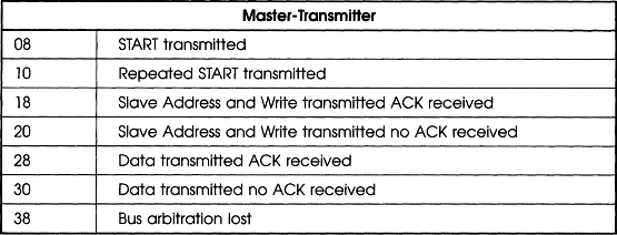
Table 5.6
S1ADR can be loaded with the 7-bit slave address to which the controller will respond if programmed as a slave receiver/transmitter. Bit 0 when set determines whether the general call address is to be recognized.
Modes of Operation
The first step must be to set interrupts with instructions such as
![]()
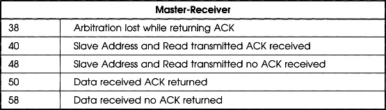
Thereafter, issuing setb sta would cause the START sequence to be commenced. Once the I2C master has determined that the bus is free for use and issued the start sequence, the SI flag will be set and the CPU should vector to location 08 as shown in Table 5.7. The code pointed to at this address should load the slave address into the S1DAT register and set the LSB according to whether the data is to be written or read. Lastly, the Interrupt Service Routine should reset SI ready for the next part of the transfer. Once acknowledge has been received from the slave, the SI flag will once again be set and the CPU will vector to either 18, 20 or 38 depending on whether the address was received, not received or lost. These vector addresses must hold code to deal with each situation appropriately (see Table 5.8).
Table 5.7

Table 5.8
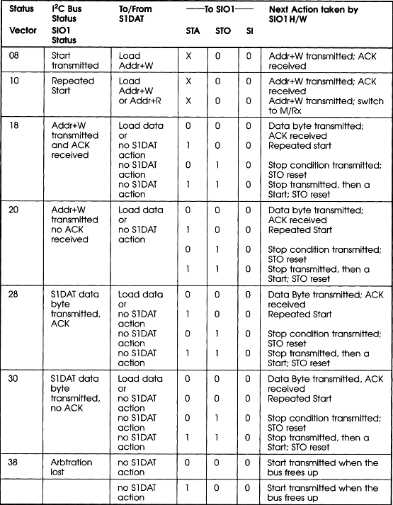
Although this seems complicated, most of the difficulty in programming is in coping with error situations. As always, software gets a bad reputation when code fails to work because the programmer did not cater for every possible outcome.
There are two other tables of data relating to the use of the ‘552 as a slave. The 8x552 data sheet from Intel or one of the second source suppliers would provide all the register data. If your own assembler is not specifically for the 8x552, then the additional SFR locations and bit names will have to be declared in an equate list.
Capture and Compare Logic
Timer 2 is connected to four 16-bit capture and three 16-bit compare registers. Capture registers save the contents of Timer T2 when a transition (0−1 or 1−0) occurs on its corresponding input pin. These are the alternate functions of Port 4 on a ‘552 and port 1 on a ‘751. To continue the analysis on the ‘751, since individual models differ in detail, essentially there are many common elements between them. If the capture facility is not needed, the four input pins can be used to generate four additional external interrupts. The capture control registers are
| CTCON | Capture Control Register |
| RTE | Reset/Toggle Enable Register |
| STE | Set Enable Register |
| TM2IR | Timer 2 Interrupt Flag Register |
| IP1 | Interrupt Priority Register |
A repeated external event such as t1, t2, t3 or t4 in Figure 5.14 can easily be measured. A capture register can be used to store the contents of T2 when the ‘start’ event occurs, and then this number can be subtracted from the updated value of T2 when the ‘stop’ event occurs.
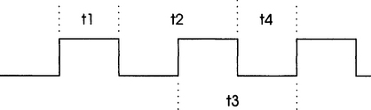

Table 5.10
Capture Control Register CTCON (E8)
| CTCON.7 | CTN3 | Capture Register 3 triggered by falling edge on CT3I |
| CTCON.6 | CTP3 | Capture Register 3 triggered by rising edge on CT3I |
| CTCON.5 | CTN2 | Capture Register 2 triggered by falling edge on CT2I |
| CTCON.4 | CTP2 | Capture Register 2 triggered by rising edge on CT2I |
| CTCON.3 | CTN1 | Capture Register 1 triggered by falling edge on CT1I |
| CTCON.2 | CTP1 | Capture Register 1 triggered by rising edge on CT1I |
| CTCON.1 | CTN0 | Capture Register 0 triggered by falling edge on CT0I |
| CTCON.0 | CTP0 | Capture Register 0 triggered by rising edge on CT0I |
Table 5.11
Reset/Toggle Enable Register RTE (EF)
| RTE.7 | TP47 | If ‘1’ then P4.7 toggles on a match between CM2 and T2 |
| RTE.6 | TP46 | If ‘1’ then P4.6 toggles on a match between CM2 and T2 |
| RTE.5 | RP45 | If ‘1’ then P4.5 is reset on a match between CM1 and T2 |
| RTE.4 | RP44 | If ‘1’ then P4.4 is reset on a match between CM1 and T2 |
| RTE.3 | RP43 | If ‘1’ then P4.3 is reset on a match between CM1 and T2 |
| RTE.2 | RP42 | If ‘1’ then P4.2 is reset on a match between CM1 and T2 |
| RTE.1 | RP41 | If ‘1’ then P4.1 is reset on a match between CM1 and T2 |
| RTE.0 | RP40 | If ‘1’ then P4.0 is reset on a match between CM1 and T2 |
Table 5.12
| STE.7 | TG47 | Toggle Flip Flops |
| STE.6 | TG47 | Toggle Flip Flops |
| STE.5 | SP45 | If ‘1’ then P4.5 is set on a match between CM0 and T2 |
| STE.4 | SP44 | If ‘1’ then P4.4 is set on a match between CM0 and T2 |
| STE.3 | SP43 | If ‘1’ then P4.3 is set on a match between CM0 and T2 |
| STE.2 | SP42 | If ‘1’ then P4.2 is set on a match between CM0 and T2 |
| STE.1 | SP41 | If ‘1’ then P4.1 is set on a match between CM0 and T2 |
| STE.0 | SP40 | If ‘1’ then P4.0 is set on a match between CM0 and T2 |
Table 5.13
| TM2IR.7 | T20V | Timer T2 16-bit overflow flag |
| TM2IR.6 | CM12 | CM2 Interrupt Flag |
| TM2IR.5 | CMI1 | CM1 Interrupt Flag |
| TM2IR.4 | CMI0 | CM0 Interrupt Flag |
| TM2IR.3 | CTI3 | CT2 Interrupt Flag |
| TM2IR.2 | CTI2 | CT2 Interrupt Flag |
| TM2IR.1 | CTI1 | CT2 Interrupt Flag |
| TM2IR.0 | CTI0 | CT2 Interrupt Flag |
Table 5.14
Timer T2 Interrupt Priority Register IP1 (F8)
| IP1.7 | PT2 | Timer T2 Overflow interrupts priority level |
| IP1.6 | PCM2 | Timer T2 Comparator 2 interrupt priority level |
| IP1.5 | PCM1 | Timer T2 Comparator 1 interrupt priority level |
| IP1.4 | PCM0 | Timer T2 Comparator 0 interrupt priority level |
| IP1.3 | PCT3 | Timer T2 Capture register 3 interrupt priority level |
| IP1.2 | PCT2 | Timer T2 Capture register 2 interrupt priority level |
| IP1.1 | PCT1 | Timer T2 Capture register 1 interrupt priority level |
| IP1.0 | PCT0 | Timer T2 Capture register 0 interrupt priority level |
A related function can be achieved with the three 16-bit compare registers. Every time that timer T2 is incremented, the new value is compared with the contents of CM0, CM1 and CM2. If a match is found then the appropriate interrupt flag in TM2IR is set.
Table 5.15
| Compare Flag | Effect | Condition IF |
| CM0 | Set Port 4 bits 0–5 | corresponding STE bits set |
| CM1 | Reset Port bits 0–5 | corresponding RTE bits set |
| CM2 | Toggles Port 4 bits 6, 7 | corresponding RTE bits set |
I2C Applications
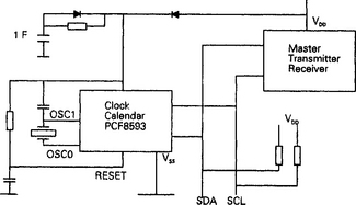
The PCF8593 Low Power Clock Calendar
A simple example can be demonstrated with the PCF8593 Low Power Clock Calendar. Like many VLSI devices, the data sheet is packed with references to the register structure and even the simplest of examples needs a detailed explanation.
This 8-pin SOIC package uses 32.768 kHz crystal as its timing reference and from this derives and maintains a track of:
Each of these has its own internal register as shown which stores the information in BCD format.
The hundredths, seconds and minutes registers are straightforward two BCD digit registers:
| tenths | hundredths | of seconds register 01 |
| tens | units | of seconds register 02 |
| tens | units | of minutes register 03 |
The hours can be set to work in 12 or 24 hour format. Register 04 is the hours register:

Register 05 handles both days 0–31 and years 0–3
| bit 7/6 | year |
| bit 5/4 | day tens |
| bit 3/0 | day units |
It assumes that year 0 is the leap year and so counts month 2 (February) up to 29.
Register 06 handles weekdays and months:
| bit 7/5 | weekdays 0–6 |
| bit 4 | month tens |
| bit 3/0 | month units |
Valid months are from 01 to 12 and it will affect the day count accordingly.
| control register | 00 |
| alarm control register | 08 |
| alarm registers | 09–0F (or free RAM locations) |
The IC operates from VDD = 2.5 to 6 V and so is suitable for both of the standard logic supply voltages (3.3 V and 5 V). With a supply current consumption of less than 100 μA, it is an ideal candidate for capacitor or battery backup applications. See Figure 5.15.

The Control Status register is as shown in Table 5.16.
Table 5.16
| D7 | Stop counting flag: | 0 count pulses; 1 stop counting |
| D6 | Hold last count flag: | 0 count; 1 store and hold last count |
| D5 | function mode | 00 clock mode 32.768 k |
| D4 | function mode | 01 clock mode 50 Hz |
| 10 event counter mode | ||
| 11 test modes | ||
| D3 | Mask flag: | 0 read R05/R06 unmasked; |
| 1 read date and month count directly | ||
| D2 | Alarm control enable: | 0 disabled; 08–0F = RAM |
| 1 enabled; 08 = alarm control register | ||
| D1 | Alarm flag | 50% duty factor minutes flag if alarm enable bit is 0 |
| D0 | Timer flag | 50% duty factor seconds flag if alarm enable bit is 0 |
The Alarm Control Register in Clock mode is an 8-bit register at location 08 (Table 5.17).
Table 5.17
| D7 | Alarm interrupt enable | 0 = alarm flag no interrupt |
| 1 = alarm flag interrupt | ||
| D6 | Timer Alarm Enable | 0 = no timer alarm |
| 1 = timer alarm | ||
| D5 | Clock alarm function | 00 no clock alarm |
| D4 | Clock alarm function | 01 daily alarm |
| 10 weekday alarm | ||
| 11 dated alarm | ||
| D3 | Timer Interrupt Enable | 0 = timer flag no interrupt |
| 1 = timer flag interrupt | ||
| D2 | Timer function | 000 no timer |
| D1 | Timer function | 001 hundreds of a second |
| D0 | Timer function | 010 seconds |
| 011 minutes | ||
| 100 hours | ||
| 101 days | ||
| 110 not used | ||
| 111 test mode: all counter in parallel |
An alarm signal is generated when the contents of the alarm registers matches exactly the contents of the involved counter registers. The year and weekday bits are ignored in a dated alarm. A daily alarm ignores the month and date bits. When a weekday alarm is selected the contents of the alarm weekday/month register (register OE) will select the weekdays on which an alarm is activated:
![]()
Programming
The PCF8593 has a fixed I2C address of 1010001x. The last bit determines whether the master is writing (0) or reading (1). Hence the addresses to be used by the master are C2H and C3H.
or
• read from the PCF8593 to determine time or date information in the following communication sequences:
To set the PCF8593 into timer mode:
![]()
C2 addresses the PCF8593 in write mode to address 00, sending data 08.
To set the time and date as 10:23:06.10 on Tuesday January 30 of a leap year:
![]()
To read the hours and minutes:
![]()
Note that under the I2C protocol, the A following the mm transmission from the slave has to be provided by the master. All the other Acknowledge As are sent from the Slave PCF 8593. An application circuit is shown in Figure 5.16.
MCS51 (80552) Software Chunks
As previously discussed, the 80552 with an I2C port would first need to have the appropriate ports set to logic 1.
![]()
It is then necessary to enable interrupts
![]()
and to start a transmission
![]()
When the I2C bus is clear, the CPU will vector to program memory 08 where there would usually be a jmp to a less congested part of program memory. This would normally be down with the subroutines at the end of the program. The ‘08’ Interrupt Service Routine has to write a ‘C2’ into the SDAT register to generate a Start condition.
![]()
If an ACKnowledge is received, all is well and the act of receiving an ACK will cause a vector to location 18H. The code at 18 will cause a jump into the Interrupt Service Routine proper. This Service routine will be called twice in our trivial example; once to send 00 and once to send 08. Thus the code is now getting more complicated, since we must devise a method of ‘remembering’ which byte we have transferred. The usual technique is to use a register or a memory location to act as a pointer to a table of data or as an offset within that table. Suppose we labelled a suitable location as setup_marker to hold a down counter:

and a table in memory could be created with the simple define byte code:
![]()
In this example, the data goes in reverse order so the Interrupt Service Routine would look something like:

As already mentioned, the difficulties come when an error condition occurs.
Receiving data is very similar, except that the ’552 has to change into a Master Receiver half way through the transmission.
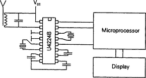
U4224B
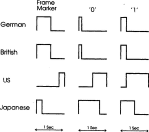
Of course, if measurement or display of time is important, then a more interesting solution is to decode time signals from the many low-frequency transmitters which operate around the world. One such IC is the U4224B from Telefunken Semiconductors. This IC is capable of decoding signals from

Each shares the same characteristic that the transmission sequence has an index count of 1 second, and during the 1 minute time frame, transmits minute, hour, day of week, day of month, year and:
| Summertime flag | (D) |
| BST flag | (UK) |
| Daylight saving information | (USA) |
| Leap year flag | (USA) |
The application circuit is quite minimal, consisting as it does of the IC, two crystals, four capacitors and a ferrite aerial. Interface to the microprocessor is by three lines, and of these, two are for U4224B control and one is the Time Code Output signal. TCO is a digital series of 0s and 1s which are distinguished by the pulse width.
The USA and Japan additionally have six 200 ms pulse width position markers every 10 seconds. The German start-of-minute frame is recognized by a missing pulse, whereas all of the others have a unique pulse width.
This section was just included for completeness for those who are interested in national transmitted standards. Decoding hardware is cheap and easy to implement.
Table 5.18

Decoding software would just rely on being able to distinguish between pulse widths and to be able to count. The data is output in BCD format and is found at the bit positions shown in Table 5.19.
Table 5.19

Figure 5.17 shows the application.