
3
Processor Elements
This chapter begins our development of a comprehensive understanding of modern processor architectures. Building upon the basic digital circuits introduced in Chapter 2, Digital Logic, we discuss the functional units of a simple, generic computer processor. Concepts related to the instruction set and register set are introduced, followed by a discussion of the steps involved in instruction loading, decoding, execution, and sequencing. Addressing modes and instruction categories are discussed in the context of the 6502 processor architecture. We choose to focus on this venerable processor for its structural cleanliness and simplicity, which allows us to consider basic concepts without distractions. The requirement for processor interrupt handling is introduced, using the example of 6502 interrupt processing. The standard approaches that modern processors employ for input/output (I/O) operations are introduced, including direct memory access (DMA).
After completing this chapter, you will understand the basic components of a processor and the structure of processor instruction sets. You will have learned the categories of processor instructions, why interrupt processing is necessary, and will have an understanding of I/O operations.
The following topics will be covered in this chapter:
- A simple processor
- The instruction set
- Addressing modes
- Instruction categories
- Interrupt processing
- Input/output operations
Technical requirements
Files for this chapter, including answers to the exercises, are available at https://github.com/PacktPublishing/Modern-Computer-Architecture-and-Organization-Second-Edition.
A simple processor
The 6502 processor architecture and a small subset of its instructions were introduced in Chapter 1, Introducing Computer Architecture. In this section, we will build upon that foundation to present some of the functional components universally employed in processor architectures, from the tiniest embedded controllers to the most powerful server CPUs.
The integrated circuit at the core of a computer system goes by a few different names: the Central Processing Unit (CPU), microprocessor, or, simply, processor. A microprocessor is a single integrated circuit that implements all the functions of a processor. This book will refer to all categories of CPUs and microprocessors as processors.
A processor like the 6502 contains three logically distinct functional units:
- The control unit manages the overall operation of the device. This includes fetching the next instruction from memory, decoding the instruction to determine the operation to perform, and distributing the execution of the instruction to appropriate elements within the processor.
- The Arithmetic Logic Unit (ALU) is a combinational circuit that performs arithmetic and bit manipulation operations.
- The register set provides source and destination locations for instruction inputs and outputs. Registers are also used as temporary storage locations.
The following diagram shows the flow of control and data among the control unit, the registers, the ALU, system memory, and input/output devices:
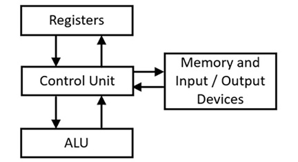
Figure 3.1: Interactions between processor functional units
The control unit directs overall processor operations to carry out each instruction. The registers, ALU, memory, and I/O devices respond to commands initiated by the control unit.
Control unit
The control unit of a modern processor is a synchronous sequential digital circuit. It interprets processor instructions and manages the execution of those instructions by interacting with the other functional units within the processor and with external components, including memory and input/output devices. The control unit is a key part of the 6502’s von Neumann architecture.
In this chapter, the term memory refers to Random Access Memory (RAM) external to the processor’s execution units. Cache memory, which often resides within a microprocessor integrated circuit, will be covered in later chapters.
Some examples of I/O devices are the computer keyboard, the mouse, disk storage, and graphical video displays. Other common I/O devices include network interfaces, Wi-Fi and Bluetooth® wireless interfaces, sound output to speakers, and microphone input.
When a computer system is powered on, the processor undergoes a reset process to initialize its internal components. Following a reset, the processor loads the Program Counter (PC) with the memory location of the first instruction to be executed. Software developers who construct the lowest-level system software components must configure their development tools to produce a code memory image that begins execution at the address required by the processor architecture.
The PC is a central component of the control unit. The PC always contains the memory address of the next instruction to be executed. At the beginning of each instruction execution cycle, the control unit reads the data word at the memory address indicated by the PC and places it in an internal register for decoding and execution. The first word of an instruction contains an opcode. Based on the opcode bit pattern, the control unit may read additional memory locations following the opcode to retrieve data needed by the instruction, such as a memory address or data operand.
As the control unit begins executing instructions, it performs the repetitive cycle shown in Figure 3.2:
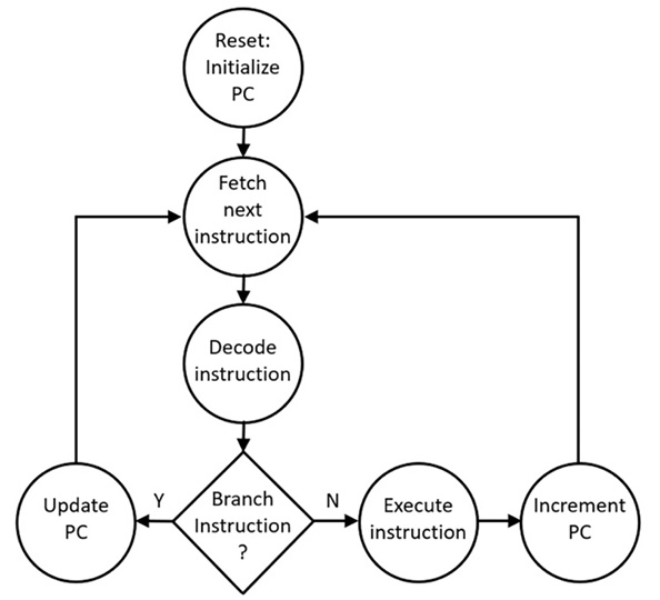
Figure 3.2: Instruction execution cycle
Following a reset, the PC contains the initial instruction location. The control unit fetches the first instruction from memory and decodes it. During decoding, the control unit determines the actions required by the instruction.
As part of the decoding process, the control unit identifies the category of instruction. The two basic instruction categories represented in Figure 3.2 are branching instructions and all other instructions. Branching instructions are implemented directly by the control unit. These instructions cause the contents of the PC to be replaced with the memory address of the branch destination. Examples of instructions that perform branching are conditional branch instructions (when the branch is taken), subroutine calls, subroutine returns, and unconditional branching (also called jump) instructions.
Instructions that do not involve branching are carried out by processor circuitry under the direction of the control unit.
In a sense, the control unit manages the execution of the non-branching instructions in a manner similar to the Analytical Engine’s mill (see Chapter 1, Introducing Computer Architecture), except, instead of using the presence of studs on a rotating barrel to engage portions of the mill machinery, the control unit uses the decoded bits of the instruction opcode to activate particular sections of digital circuitry. The selected circuit components perform the tasks required by the instruction.
The process of instruction execution may include actions such as reading or writing a register, reading or writing a memory location, directing the ALU to perform a mathematical operation, or other miscellaneous activities.
In most processors, the execution of a single instruction extends over multiple processor clock cycles. The instruction cycle count can vary significantly from simple instructions that require a small number of clock cycles to complex operations that take many cycles to complete. The control unit orchestrates all this activity.
The circuits managed by the control unit are constructed from the simple logic gates discussed in Chapter 2, Digital Logic, and are often composed of higher-level constructs such as multiplexers, latches, and flip-flops. Multiplexers, in particular, are commonly used by control unit logic to selectively route data to a particular destination.
Executing an instruction – a simple example
Consider a simplified example of two 6502 instructions, TXA and TYA. TXA copies the contents of register X to register A, and TYA does the same thing using the Y register as the source. If we consider these two instructions in isolation, the execution of both instructions can be implemented as shown in Figure 3.3:
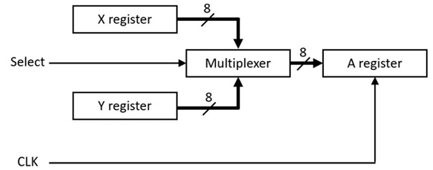
Figure 3.3: 6502 TXA and TYA instructions
The circuit in Figure 3.3 assumes the X and Y registers are D flip-flop registers (as in Figure 2.14), except in the 6502 they are 8-bit registers rather than 4 bits. The multiplexer is implemented as eight copies of the two-input, single-bit multiplexer of Figure 2.9, all controlled by a single shared selector input. In Figure 3.3, thicker lines represent 8-bit data buses and thinner lines are individual logic signals. The short lines crossing the thick lines with the numeral 8 above them indicate the number of bits in the bus.
To execute the TXA instruction, the following steps are performed:
- The control unit first sets the Select input to direct the X register data bits through to the output of the multiplexer. This presents the data from X at the inputs to the A register.
- After the Select input to the multiplexer has been set, the control unit must pause to permit the propagation of the data bits to the multiplexer outputs.
- After the multiplexer outputs have stabilized, the control unit generates a rising edge on the CLK signal to load the X register data bits into register A.
To execute the TYA instruction, the control unit performs the same sequence of steps, except it must first set the Select input to feed the Y register to the multiplexer output.
This is a very simple example of a control unit instruction operation, but it demonstrates that an individual instruction may consist of multiple steps and may involve just a small portion of the logic circuits present in the processor. Unused components within the processor must be managed by the control unit to ensure that they remain idle when not needed to execute an instruction. This prevents those components from interfering with the executing instruction and keeps power consumption to a minimum.
Arithmetic logic unit
The ALU performs arithmetic and bit-oriented operations under the direction of the control unit. To perform an operation, the ALU requires data input values, called operands, along with a code indicating the operation to be performed. The ALU output is the result of the operation. ALU operations may use one or more processor flags, such as the carry flag, as input, and set the states of processor flags as outputs. In the 6502, ALU operations update the carry, negative, zero, and overflow flags.
An ALU is a combinational circuit, which implies its outputs update asynchronously in response to changes at the inputs and it retains no memory of previous operations.
To execute an instruction involving the ALU, the control unit applies inputs to the ALU, pauses to allow for the propagation delay across the ALU, and then transfers the ALU output to the destination specified by the instruction.
The ALU contains an adder circuit to perform addition and subtraction operations. In a processor with two’s complement arithmetic, subtraction can be implemented by first performing a two’s complement negation of the right operand and adding the result to the left operand. Mathematically, when performing subtraction in this manner, the expression A-B is transformed into A+(-B).
As you’ll recall from Chapter 1, Introducing Computer Architecture, the two’s complement negation of a signed number is achieved by inverting all the bits in the operand and adding 1 to the result. Incorporating this operation, subtraction represented as A+(-B) becomes A+(NOT(B)+1).
Looking at subtraction in this form should clarify the use of the 6502 carry flag in conjunction with the SBC instruction. The C flag provides the “+1” in subtraction when there is no borrow. If there is a borrow, the sum must be reduced by 1, which is accomplished by setting the C flag to 0.
To summarize, in the 6502, subtraction logic is identical to addition logic with the single difference that the B operand in A-B is routed through a set of NOT gates to invert all eight of the bits prior to feeding NOT(B) to the adder input.
Figure 3.4 is a functional representation of the addition and subtraction operations in the 6502:

Figure 3.4: 6502 addition and subtraction operations
Similar to Figure 3.3, Figure 3.4 is a highly simplified representation of the 6502 processor depicting only the components involved in the ADC and SBC instructions. The Select input in Figure 3.4 chooses whether the operation is addition or subtraction. Addition requires selecting the upper multiplexer input, while the lower multiplexer input selects subtraction. In the 6502 architecture, the A register is always the left operand for subtraction.
The inputs to the adder are the left and right operands and the C flag. When executing an ADC or SBC instruction, the control unit presents the right operand to the multiplexer data inputs and sets the multiplexer select input to the appropriate state for the given instruction. After pausing for propagation through the NOT gate, the multiplexer, and the adder, the control unit generates a clock edge that latches the adder outputs into the A register and the processor flags register.
The processor flags are set as shown in the following execution of an ADC or SBC instruction:
- C indicates whether an addition generated in a carry (C = 1) or whether a subtraction produced a borrow (C = 0).
- N contains the value of bit 7 of the result.
- V indicates whether a signed overflow occurred (V = 1 if overflow occurred).
- Z is 1 if the result is zero. Z is 0 otherwise.
An ALU supports a variety of operations in addition to adding and subtracting two numbers. In the 6502, most operations with two operands use the A register as the left operand. The right operand is either read from a memory location or provided as an immediate value in the next memory location after the opcode. All 6502 ALU operands and results are 8-bit values. The 6502 ALU operations are as follows:
ADC,SBC: Add or subtract two operands with carry input.DEC,DEX,DEY: Decrement a memory location or register by one.INC,INX,INY: Increment a memory location or register by one.AND: Perform a bitwise logical AND operation on two operands.ORA: Perform a bitwise logical OR operation on two operands.EOR: Perform a bitwise logical XOR operation on two operands.ASL,LSR: Shift the A register or memory location left or right by one bit position and insert 0 into the vacated bit position.ROL,ROR: Rotate the A register or memory location left or right by one bit position and insert the C flag value into the vacated bit position.CMP,CPX,CPY: Subtract two operands and discard the result, setting the N, Z, and C flags based on the result of the subtraction.BIT: Perform a bitwise logical AND between two operands and use the Z flag to indicate whether the result is 0. In addition, copy bits 7 and 6 of the left operand to the N and V flags.
The 6502 has limited ALU capabilities when compared to more complex modern processors such as the x86 family.
For example, in the 6502, the programmer must implement multiplication and division in code as repetitive addition and subtraction operations. Also, the 6502 can shift or rotate a value by just one bit position per instruction.
The x86, on the other hand, directly implements multiplication and division instructions, and the x86 shift and rotate instructions include a parameter indicating the number of bit positions to shift in a single instruction.
An ALU is a necessarily complex logic device, making it an ideal candidate for design with a hardware design language. The following listing is a VHDL implementation of a portion of a 6502-like ALU:
-- Load the standard libraries
library IEEE;
  use IEEE.STD_LOGIC_1164.ALL;
  use IEEE.NUMERIC_STD.ALL;
-- Define the 8-bit ALU inputs and outputs
entity ALU is
  port (
    -- Left operand
    LEFT        : in    std_logic_vector(7 downto 0);
    -- Right operand
    RIGHT       : in    std_logic_vector(7 downto 0);
    -- ALU operation
    OPCODE      : in    std_logic_vector(3 downto 0);
    -- Carry input
    C_IN        : in    std_logic;
    -- ALU output
    RESULT      : out   std_logic_vector(7 downto 0);
    -- Carry output
    C_OUT       : out   std_logic;
    -- Negative flag output
    N_OUT       : out   std_logic;
    -- Overflow flag output
    V_OUT       : out   std_logic;
    -- Zero flag output
    Z_OUT       : out   std_logic
  );
end entity ALU;
-- Define the behavior of the 8-bit ALU
architecture BEHAVIORAL of ALU is
begin
  P_ALU : process (LEFT, RIGHT, OPCODE, C_IN) is
    variable result8  : unsigned(7 downto 0);
    variable result9  : unsigned(8 downto 0);
    variable right_op : unsigned(7 downto 0);
  begin
    case OPCODE is
      when "0000" | "0001" => -- Addition or subtraction
        if (OPCODE = "0000") then
          right_op := unsigned(RIGHT);     -- Addition
        else
          right_op := unsigned(not RIGHT); -- Subtraction
        end if;
        result9 := ('0' & unsigned(LEFT)) +
                   unsigned(right_op) +
                   unsigned(std_logic_vector'(""& C_IN));
        result8 := result9(7 downto 0);
        C_OUT <= result9(8);               -- C flag
        -- V flag
        if (((LEFT(7) XOR result8(7)) = '1') AND
            ((right_op(7) XOR result8(7)) = '1')) then
          V_OUT <= '1';
        else
          V_OUT <= '0';
        end if;
      when "0010" =>                          -- Increment
        result8 := unsigned(LEFT) + 1;
      when "0011" =>                          -- Decrement
        result8 := unsigned(LEFT) - 1;
      when "0101" =>                          -- Bitwise AND
        result8 := unsigned(LEFT and RIGHT);
      when "0110" =>                          -- Bitwise OR
        result8 := unsigned(LEFT or RIGHT);
      when "0111" =>                          -- Bitwise XOR
        result8 := unsigned(LEFT xor RIGHT);
      when others =>
        result8 := (others => 'X');
    end case;
    RESULT <= std_logic_vector(result8);
    N_OUT <= result8(7);                      -- N flag
    if (result8 = 0) then                     -- Z flag
      Z_OUT <= '1';
    else
      Z_OUT <= '0';
    end if;
  end process P_ALU;
end architecture BEHAVIORAL;
This code defines a simple ALU as a combinational circuit with a left operand, right operand, opcode, and the C flag as its inputs. The outputs are the result of the operation along with the C, N, V, and Z flags.
Next, we’ll look at the purpose and functions of processor registers.
Registers
Processor registers are internal storage locations that serve as sources and destinations for instruction operations. Registers provide the quickest data access in a processor but are limited to a very small number of locations due to their high cost in terms of die area. The width of a register in bits is generally the same as the processor word size.
The 6502, as we have seen, has only three 8-bit registers: A, X, and Y. The x86 has six 32-bit registers suitable for temporary data storage: EAX, EBX, ECX, EDX, ESI, and EDI. In many processor architectures, specific registers are assigned to provide inputs required by certain instructions. For example, in the x86 architecture, a single REP MOVSD instruction moves a block of data with the length (in words) in ECX beginning at the source address in ESI to the destination address in EDI.
When designing a new processor architecture, it is critical to evaluate the trade-off between the number of registers and the number and complexity of instructions available to the processor. For a given integrated circuit die size and fabrication process (which together constrain the number of transistors available for the processor), adding more registers to the architecture reduces the number of transistors available for executing instructions and for performing other functions. In contrast, adding instructions with complex capabilities may limit the die space available for registers. This tension between instruction set complexity and the number of registers is expressed in the categorization of an architecture as CISC or RISC:
- CISC (Complex Instruction Set Computer) processors are characterized as having a rich instruction set providing a variety of features, such as the ability to load operands from memory, perform an operation, and store the result to memory, all in one instruction. In a CISC processor, an instruction may take many clock cycles to execute as the processor performs all required subtasks. The
REPMOVSDinstruction mentioned previously is an example of a single instruction with a potentially lengthy execution time. CISC processors tend to have a smaller number of registers due, in part, to the die space required for the circuitry occupied by the instruction set logic. The x86 is a classic example of CISC architecture. - RISC (Reduced Instruction Set Computer) processors, on the other hand, have a smaller number of instructions that each perform simpler tasks in comparison to CISC instructions. Performing an operation on data values stored in memory might require a pair of load instructions to load two operands from memory into registers, another instruction to perform the operation, and a final instruction to store the result back to memory.
The key distinction between CISC and RISC is that RISC architectures are optimized to execute individual instructions at very high speed. Even though reading memory, performing the operation, and writing the result back to memory require several more instructions in an RISC processor than in a CISC processor, the overall start-to-finish time may be comparable or even faster for the RISC processor. Some examples of RISC architectures are ARM, discussed in Chapter 10, Modern Processor Architectures and Instruction Sets, and RISC-V, discussed in Chapter 11, The RISC-V Architecture and Instruction Set.
The reduction in instruction set complexity in RISC processors leaves more die space for registers, which means there is generally a larger number of registers in RISC processors in comparison to CISC processors. The ARM architecture, for example, has 13 general-purpose registers, while the RISC-V base 32-bit architecture has 31 general-purpose registers.
The larger number of registers in RISC architectures reduces the need to access system memory because more registers are available for storing intermediate results. This improves performance because accessing system memory is significantly more time-consuming than accessing data located in processor registers.
Think of a processor register as a set of D flip-flops in which each flip-flop contains one bit of the register’s data. Each of a register’s flip-flops is loaded with data by a common clock signal. Input to a register may arrive at the flip-flops after passing through a multiplexer that selects one of potentially many data sources under the control of the executing instruction.
As an alternative to using a multiplexer for this purpose, an instruction may load a register from a data bus internal to the processor. In this configuration, the control unit manages the internal bus to ensure that only the desired data source is driving the data bus lines during the clock edge that loads the register, while all other data sources on the bus are inhibited from placing data on the bus.
The following sections will introduce the full range of instructions in a processor instruction set and the addressing modes used by them.
The instruction set
Similar instructions to those discussed earlier are implemented within most general-purpose processor architectures, though more sophisticated processors augment their capabilities with additional categories of instructions. The more advanced instructions available in modern processor architectures will be introduced in later chapters.
CISC processors generally support multiple addressing modes. Addressing modes are designed to enable efficient access to sequential memory locations for use by software algorithms running on the processor. The next section describes the instruction addressing modes implemented by the 6502 processor. The section following that will introduce the categories of instructions implemented by the 6502, most of which are represented in modern processor architectures. Specialized instructions for processing interrupts and for input/output operations will then be covered, including an explanation of processor features that enable high-performance input and output operations on sizable blocks of data.
Addressing modes
CISC processors support multiple addressing modes for instructions that require transferring data between memory and registers. RISC processors have a more limited number of addressing modes. Each processor architecture defines its collection of addressing modes based on an analysis of the anticipated memory access patterns that software will use on that architecture.
To introduce the 6502 addressing modes, this section employs a simple example of 6502 code that adds together four data bytes. To avoid extraneous details, the example will ignore any carry from the 8-bit sum.
Immediate addressing mode
In immediate addressing, the operand value immediately follows the opcode in memory. For the first example, assume we are given the values of the four bytes to sum and asked to write a 6502 program to perform that task. This allows us to enter the byte values directly into our code. The bytes in this example are $01 through $04. We’ll be adding the bytes together in reverse order ($04 down to $01) in anticipation of the use of a looping construct later in this section. This code uses the immediate addressing mode to add the four bytes together:
; Add four bytes together using immediate addressing mode
LDA #$04
CLC
ADC #$03
ADC #$02
ADC #$01
Notice that assembly language comments begin with a semicolon character. When these instructions finish execution, the A register will hold the value $0A, the sum of the four bytes listed as operands.
Recall from Chapter 1, Introducing Computer Architecture, that in 6502 assembly language, an immediate value is preceded by a # character and the $ character indicates the value is hexadecimal. An immediately addressed operand is read from the memory address following the instruction opcode. Immediate addressing is handy because there is no need to reserve the memory location from which to read the operand. However, immediate addressing mode is only useful when the data value is known at the time the program is written.
Absolute addressing mode
Absolute addressing mode, sometimes called direct addressing mode, specifies the memory location containing the value to be read or written by the instruction. The 6502 has 16 address bits, so an address field that supports accessing all available memory is two bytes long. A complete instruction to access data at an arbitrary 6502 memory location consists of three bytes: the first byte is the opcode, followed by two bytes for the address to be read or written. The two address bytes must be stored with the lower-order byte first, followed by the higher-order byte. The high-order byte of a 16-bit value contains the most significant 8 bits, and the low-order byte contains the least significant 8 bits.
The convention of storing the lower-order byte of a two-byte address at the lower memory address makes the 6502 a little-endian processor. The x86 is also little-endian. The ARM and RISC-V architectures allow the selection of big- or little-endian mode under software control (this is called bi-endianness), but most operating systems running on these architectures select little-endian mode.
For the absolute addressing mode example, we begin with some setup code to store the four bytes to be added together into addresses $200 through $203. The instructions to add the four bytes follow the setup code. This example uses absolute addressing mode to sum the four bytes:
; Initialize the data in memory
LDA #$04
STA $0203
LDA #$03
STA $0202
LDA #$02
STA $0201
LDA #$01
STA $0200
; Add four bytes together using absolute addressing mode
LDA $0203
CLC
ADC $0202
ADC $0201
ADC $0200
Unlike immediate addressing mode, absolute addressing permits summing four values that are not known until the time of program execution: the ADC instructions will add together whatever values have been stored in locations $200-$203. A limitation of this addressing mode is that the addresses of the bytes to be added must be specified when the program is written. This code cannot sum bytes located at an arbitrary location in memory.
Our simple example has the downside of unnecessarily stringing together a sequence of nearly identical instructions. To avoid this, it is usually desirable to place a repetitive sequence of code into a loop construct. The next two examples use a 6502 addressing mode that facilitates looping operations, although we won’t implement a loop until the second example.
Absolute indexed addressing mode
Absolute indexed addressing mode computes a memory address by adding a base address provided in the instruction to a value contained in the X or Y register. The following example adds the bytes at addresses $0200 through $0203 using absolute indexed addressing. The X register provides an offset from the base of the byte array at address $0200:
; Initialize the data in memory
LDA #$04
STA $0203
LDA #$03
STA $0202
LDA #$02
STA $0201
LDA #$01
STA $0200
; Add four bytes together using absolute indexed addressing mode
LDX #$03
CLC
LDA $0200, X
DEX
ADC $0200, X
DEX
ADC $0200, X
DEX
ADC $0200, X
The DEX instruction decrements (subtracts 1 from) the X register. Although this code makes things worse in terms of increasing the number of instructions it takes to add the four bytes together, we see that the instruction sequence DEX followed by ADC $0200, X now repeats three times.
We can use conditional branching to perform the same addition sequence in a loop:
; Initialize the data in memory
LDA #$04
STA $0203
LDA #$03
STA $0202
LDA #$02
STA $0201
LDA #$01
STA $0200
; Add four bytes together using absolute indexed addressing mode
LDX #$03
LDA $0200, X
DEX
CLC
ADD_LOOP:
ADC $0200, X
DEX
BPL ADD_LOOP
The BPL instructions means “branch on plus,” which conditionally transfers control to the instruction preceded by the ADD_LOOP label. BPL executes the branch only when the processor N flag is clear. If the N flag is set, BPL continues with the next instruction in memory.
The code in this example might not seem to have been worth the effort involved in constructing a loop just to add up four bytes. However, note that this version can be modified to add together 100 sequential bytes by simply changing the operand of the LDX instruction. Extending the previous example to add 100 bytes together in the same manner would require quite a bit more work, and the instructions would consume far more memory.
This example has the same limitation as the absolute address mode example, both of which set the start of the byte array at a memory location defined at the time the program was written. The next addressing mode removes this limitation and sums an array of bytes, starting at any address in memory.
Indirect indexed addressing mode
Indirect indexed addressing mode uses a two-byte address stored in the memory address range $00-$FF as the base address and adds the contents of the Y register to that base to produce the memory address used by the instruction. In the following example, the base address of the byte array ($0200) is first stored in little-endian order at addresses $0010 and $0011. The code uses indirect indexed addressing in a loop to add the bytes together:
; Initialize the data in memory
LDA #$04
STA $0203
LDA #$03
STA $0202
LDA #$02
STA $0201
LDA #$01
STA $0200
; Initialize the pointer to the byte array
LDA #$00
STA $10
LDA #$02
STA $11
; Add four bytes together using indirect indexed addressing mode
LDY #$03
LDA ($10), Y
DEY
CLC
ADD_LOOP:
ADC ($10), Y
DEY
BPL ADD_LOOP
With indirect indexed addressing, any memory address can be stored at addresses $10-$11 before the summing code executes. Note that indirect indexed addressing must use the Y register as the address offset. The X register is not available for use in this addressing mode.
The 6502 has some other addressing modes available: zero-page addressing mode provides instructions that are smaller (one byte less in length) and faster to execute for absolute and absolute indexed addressing by working only with memory addresses in the range $00-$FF. The term zero-page refers to the high byte of the 16-bit address, which is zero for addresses in this range. Other than exhibiting improved performance in terms of faster execution speed and reduced code memory usage, the zero-page addressing modes behave the same as the corresponding addressing modes described earlier.
Another mode is called indexed indirect addressing mode, which is like indirect indexed addressing except that the X register is used instead of Y, and the offset contained in X is added to the address provided in the instruction to determine the address of the pointer to the data. For example, assume that X contains the value 8. The LDA ($10, X) instruction adds the contents of X to $10, producing the result $18. The instruction then uses the 16-bit memory address read from addresses $18-$19 as the target memory address for loading the A register.
Indexed indirect addressing is not relevant to our example summing a sequence of bytes. One example application of this mode is selecting a value from a sequential list of pointers, where each pointer contains the address of a character string. The X register can reference one of the strings as an offset from the beginning of the pointer list. An instruction such as LDA ($10, X) will load the address of the selected string into A.
The addressing modes available in CISC processor architectures and, to a lesser degree, in RISC architectures are intended to support efficient methods of accessing various types of data structures in system memory.
The next section discusses the categories of instructions implemented in the 6502 architecture and how each instruction makes use of the available addressing modes.
Instruction categories
This section presents the categories of instructions available in the 6502 processor. The purpose of discussing the 6502 here is to introduce the concepts associated with the instruction set of a processor architecture that is simpler than the modern 32- and 64-bit processors we will examine in later chapters. By the time we get to those processors, the underlying instruction set concepts should be quite familiar.
Memory load and store instructions
The 6502 uses load and store instructions to read data values from system memory into processor registers and to write registers out to system memory. In the 6502 architecture, the LDA, LDX, and LDY instructions load the register identified in the instruction mnemonic with an 8-bit word from system memory. LDA supports all addressing modes available in the 6502, while LDX and LDY each support a more limited subset of addressing modes: immediate, absolute, and absolute indexed.
After each of these instructions finishes executing, the N and Z flags indicate whether the value that was loaded is negative (that is, bit 7 is set) and whether the value is zero.
STA, STX, and STY store the register identified in the instruction to memory. Each store instruction supports the same addressing modes as the load instruction for that register, except the store instructions do not support immediate addressing mode. These instructions update the N and Z flags to reflect the value stored.
Register-to-register data transfer instructions
These instructions copy an 8-bit word from one of the A, X, and Y registers to another register. These instructions use implied addressing mode, which means the source and destination of each instruction are indicated directly by the instruction opcode.
TAX copies the A register contents to the X register. TAY, TXA, and TYA perform similar operations between the register pairs indicated by the instruction mnemonic. These instructions update the N and Z flags.
Stack instructions
The TXS instruction copies the X register to the stack pointer (S) register. This instruction must be used to initialize the S register during system startup. TSX copies the S register to the X register. TSX updates the N and Z flags. TXS does not affect any flags.
PHA pushes the A register contents onto the stack. PHP pushes the processor flags onto the stack as an 8-bit word. These instructions do not affect the processor flags. Pushing a value onto the stack consists of writing the register to the memory address computed by adding $100 to the S register and then decrementing the S register.
PLA and PLP pop the A register and the flags register from the stack, respectively. Popping a value first increments the S register and then transfers the value at the location computed by adding $100 to the S register to the target register location.
PLA updates the N and Z flags. PLP sets or clears six of the seven processor flags based on the value popped from the stack. The B (break) flag is only meaningful in a copy of the processor flags register that has been pushed onto the stack by an interrupt or by the PHP instruction. This distinguishes a BRK instruction from a hardware interrupt request. Both the PHP and BRK instructions push the flags register with the B bit (bit 4) set.
Hardware interrupts generated via the processor ![]() (Interrupt Request) and
(Interrupt Request) and ![]() (Non-Maskable Interrupt) pins push the processor flags register with the B bit cleared. Interrupt processing and the
(Non-Maskable Interrupt) pins push the processor flags register with the B bit cleared. Interrupt processing and the BRK instruction will be discussed later in this chapter.
Arithmetic instructions
As we’ve seen, addition and subtraction are performed by the ADC and SBC instructions. The left operand of each instruction is the A register, which is also the destination for the result of the operation. All addressing modes are available for designating the right operand. The Z, C, N, and V flags are updated to reflect the result of the operation.
INC and DEC, respectively, increment or decrement the specified memory location by adding 1 to, or subtracting 1 from, the value at that location. The result is stored at the same memory location. Absolute and absolute indexed addressing modes are supported. These instructions update the N and Z flags based on the result of the operation.
The INX, DEX, INY, and DEY instructions increment or decrement the X or Y register, as indicated by the mnemonic. These instructions update the N and Z flags.
The CMP instruction performs a comparison by subtracting the operand value from the A register. The behavior of CMP is very similar to the instruction sequence SEC followed by SBC. The N, Z, and C flags are set to reflect the result of the subtraction. The differences between CMP and SBC are as follows:
CMPdiscards the result of the subtraction (the value in A is unaffected by theCMPinstruction)CMPdoes not use decimal mode if the D flag is setCMPdoes not affect the value of the V flagCMPsupports all addressing modes
The CPX and CPY instructions are like CMP, except the X or Y register is used as the left operand as indicated in the mnemonic, and only absolute and absolute indexed addressing modes are supported for the right operand.
Logical instructions
The AND, EOR, and ORA instructions perform bitwise AND, XOR, and OR operations, respectively, between the A register and the operand. The result is stored in the A register. The Z and N flags are updated to reflect the result of the operation. All addressing modes are supported.
The ASL instruction shifts the operand one bit left, inserting a zero as the least significant bit. The most significant bit is shifted into the C flag. This is equivalent to multiplying the A register by two and placing the most significant bit of the 9-bit result in C.
Similar to ASL, LSR shifts the operand one bit right, inserting a zero as the most significant bit. The least significant bit is shifted into the C flag. This is equivalent to the division of an unsigned operand by two, with the remainder placed in C.
The ROL and ROR instructions shift the A register one bit to the left or right, respectively. The previous value of the C flag is shifted into the bit location vacated by the shift operation. The bit shifted out of A is stored in the C flag.
ASL, LSR, ROL, and ROR support accumulator addressing mode, which uses the A register as the operand. This mode is specified by using the special operand value “A,” as in ASL A. These four instructions also support absolute and absolute indexed addressing modes.
The BIT instruction performs a bitwise AND between the operand and the A register, and the result is discarded. The Z flag is updated based on the result of this operation. Bits 7 and 6 from the memory location are copied to the N and V flags, respectively. Only absolute addressing mode is supported.
Branching instructions
The JMP instruction loads the operand into the PC and continues execution with the instruction at that location. The destination, a two-byte absolute address, can be anywhere in the 6502’s address space:
- The
BCCandBCSinstructions perform conditional branching if the C flag is clear or set, respectively - The
BNEandBEQinstructions perform conditional branching if the Z flag is clear or set, respectively - The
BPLandBMIinstructions perform conditional branching if the N flag is clear or set, respectively - The
BVCandBVSinstructions perform conditional branching if the V flag is clear or set, respectively
The conditional branch instructions use relative addressing mode, where the target address is a signed 8-bit offset (in the range -128 to +127 bytes) from the address of the instruction following the branch instruction.
Subroutine call and return instructions
The JSR instruction pushes the address of the instruction following the JSR instruction (minus one) onto the stack, loads the address provided as the 16-bit operand into the PC, and then continues execution from the instruction at that location.
RTS is used to end a subroutine. The return PC value (minus one) is pulled from the stack and loaded into the PC. The RTS instruction increments the PC before it is used as the address of the next instruction to execute.
Processor flag instructions
The processor flag instructions operate directly on the flags, setting or clearing a single flag.
- The
SECandCLCinstructions set and clear the C flag, respectively. - The
SEDandCLDinstructions set and clear the D flag, respectively. - The
CLVinstruction clears the V flag. No instruction simply sets the V flag.
Interrupt-related instructions
Interrupt-related instructions allow the processor to manage the handling of externally generated interrupts and to generate software-triggered interrupts. External interrupts can be of two types: maskable and non-maskable. Each interrupt type is triggered by its own input pin on the 6502 processor.
Maskable interrupts can be disabled by setting the processor I flag. When masked, the processor ignores the associated input pin. Non-maskable interrupts, as the name implies, cannot be inhibited and will always initiate a processor interrupt when the appropriate signal transition occurs on the associated pin. We’ll cover interrupt processing in more detail in an upcoming section.
The SEI and CLI instructions set and clear the I flag, respectively. When the I flag is set, maskable interrupts are disabled, or masked.
The BRK instruction triggers a non-maskable interrupt. The memory address two bytes after the BRK instruction is pushed onto the stack, followed by the processor flags register. The PC is loaded with the interrupt handler address, which is read from memory addresses $FFFE-$FFFF. The interrupt handler then begins to execute.
The BRK instruction does not alter any register contents (other than the stack pointer) or processor flags. The flags register pushed onto the stack has the B bit set to indicate that the interrupt is the result of a BRK instruction.
RTI returns from an interrupt handler. This instruction restores the processor flags from the stack and restores the PC. After the processor flags have been restored, the B flag is not meaningful and should be ignored.
Interrupt processing and the use of the BRK instruction will be discussed further in the Interrupt processing section of this chapter.
No operation instruction
The NOP instruction (often referred to as no-op) does nothing except advance the PC to the following instruction.
NOP instructions are sometimes used as a debugging tool during program development. For example, one or more instructions can be effectively “commented out” by filling the memory addresses for those instructions with $EA bytes. $EA is the hexadecimal value of the 6502 NOP opcode.
Interrupt processing
Processors generally support some form of interrupt handling for responding to service requests from external devices. Conceptually, interrupt handling resembles a scenario in which you are busy working on a task and your phone rings. After answering the call and perhaps jotting a note for later action (“buy bread,” for example), you resume the interrupted task. We humans employ several similar mechanisms, such as doorbells and alarm clocks, which enable us to interrupt lower priority activities and respond to more immediate needs.
 processing
The 6502 integrated circuit has two input signals that allow external components to notify the processor of a need for attention. The first is the interrupt request input, ![]() .
. ![]() is an active low (meaning the signal is at its low, or 0, level; that’s what the bar over the IRQ characters means) input that generates a processor interrupt when pulled low. Think of this signal as a telephone ringer notifying the processor of an incoming call.
is an active low (meaning the signal is at its low, or 0, level; that’s what the bar over the IRQ characters means) input that generates a processor interrupt when pulled low. Think of this signal as a telephone ringer notifying the processor of an incoming call.
The 6502 cannot respond instantly to a low signal level on the ![]() input. Before the 6502 can begin to process the interrupt, it must first complete the instruction already in progress. Next, it pushes the return address (the address of the next instruction that would have been executed after the instruction in progress) onto the stack, followed by the processor flags register. Since this interrupt was generated by the
input. Before the 6502 can begin to process the interrupt, it must first complete the instruction already in progress. Next, it pushes the return address (the address of the next instruction that would have been executed after the instruction in progress) onto the stack, followed by the processor flags register. Since this interrupt was generated by the ![]() input, the B flag in the processor flags on the stack will be 0.
input, the B flag in the processor flags on the stack will be 0.
Unlike the JSR instruction, the return address pushed in response to the ![]() input is the actual address of the next instruction to be executed, rather than the instruction address minus 1. The interrupt return address will not be incremented to generate the return address as occurs during
input is the actual address of the next instruction to be executed, rather than the instruction address minus 1. The interrupt return address will not be incremented to generate the return address as occurs during RTS instruction execution.
In the next stage of interrupt processing, the processor loads the address of the ![]() handler routine from memory addresses
handler routine from memory addresses $FFFE-$FFFF into the PC. The 6502 then begins executing the interrupt handler code at that address. The interrupt handler is the code that identifies the peripheral that initiated the interrupt and performs the processing required to satisfy the request, and then returns control to the code that was executing prior to the interrupt.
When the interrupt handler is finished, it executes the RTI instruction. RTI pops the processor flags and the PC from the stack and resumes execution at the instruction following the instruction that was in progress when the ![]() input was driven low.
input was driven low.
The ![]() input is a maskable interrupt, meaning it is possible to perform the equivalent of putting the telephone ringer on mute. When
input is a maskable interrupt, meaning it is possible to perform the equivalent of putting the telephone ringer on mute. When ![]() processing begins, the 6502 automatically sets the I flag, which masks (disables) the
processing begins, the 6502 automatically sets the I flag, which masks (disables) the ![]() input until the I flag is cleared.
input until the I flag is cleared.
The I flag will be cleared when the RTI instruction restores the processor flags because the I flag could not have been set when the processor began responding to the ![]() . The I flag can also be cleared by the
. The I flag can also be cleared by the CLI instruction, which means it is possible to enable ![]() interrupts while processing an
interrupts while processing an ![]() interrupt. An interrupt handled while processing another interrupt is referred to as a nested interrupt.
interrupt. An interrupt handled while processing another interrupt is referred to as a nested interrupt.
The ![]() input is level-sensitive, which means any time the
input is level-sensitive, which means any time the ![]() input is low and the I flag is cleared, the processor will initiate the interrupt processing sequence. One consequence of this is that, at the completion of processing an interrupt, the 6502’s interactions with the interrupt source must ensure that the
input is low and the I flag is cleared, the processor will initiate the interrupt processing sequence. One consequence of this is that, at the completion of processing an interrupt, the 6502’s interactions with the interrupt source must ensure that the ![]() input is no longer low. If
input is no longer low. If ![]() remains low when the
remains low when the RTI instruction is executed, the 6502 will immediately begin the interrupt handling process all over again.
Interrupts initiated via the ![]() input handle most routine interactions between the 6502 and peripheral devices. For example, the keyboard is an interrupt source in most computers.
input handle most routine interactions between the 6502 and peripheral devices. For example, the keyboard is an interrupt source in most computers.
Each keypress generates an ![]() interrupt. During keyboard interrupt processing, the 6502 reads the identification of the key from the keyboard interface and stores it into a queue for later processing by the currently active application. The
interrupt. During keyboard interrupt processing, the 6502 reads the identification of the key from the keyboard interface and stores it into a queue for later processing by the currently active application. The ![]() handler code does not need to know anything about what the key press information will be used for; it just saves the data for later use.
handler code does not need to know anything about what the key press information will be used for; it just saves the data for later use.
 processing
The second interrupt input to the 6502 is the non-maskable interrupt, ![]() . As its name implies, the
. As its name implies, the ![]() input is not masked by the I flag.
input is not masked by the I flag. ![]() is an edge-sensitive input that triggers on the falling edge of the signal.
is an edge-sensitive input that triggers on the falling edge of the signal.
The processing of ![]() interrupts is similar to the processing of
interrupts is similar to the processing of ![]() interrupts, except the address of the interrupt handler routine is loaded from memory addresses
interrupts, except the address of the interrupt handler routine is loaded from memory addresses $FFFA-$FFFB and the I flag has no effect on this type of interrupt.
Because ![]() is non-maskable, it can be triggered at any time, including when the 6502 is in the middle of handling an
is non-maskable, it can be triggered at any time, including when the 6502 is in the middle of handling an ![]() interrupt, or even while handling an earlier
interrupt, or even while handling an earlier ![]() interrupt.
interrupt.
The ![]() input is normally reserved for very high-priority conditions that cannot be delayed or missed. One possible use of
input is normally reserved for very high-priority conditions that cannot be delayed or missed. One possible use of ![]() interrupts is to trigger the incrementing of a real-time clock at regular intervals.
interrupts is to trigger the incrementing of a real-time clock at regular intervals.
This example of ![]() handler code increments a 32-bit clock counter located at addresses
handler code increments a 32-bit clock counter located at addresses $10-$13 each time the interrupt occurs:
; Increment a 32-bit clock counter at each /NMI interrupt
NMI_HANDLER:
INC $10
BNE NMI_DONE
INC $11
BNE NMI_DONE
INC $12
BNE NMI_DONE
INC $13
NMI_DONE:
RTI
When referring to hardware signals in program source code, a leading forward slash can be used to indicate an active low signal. ![]() is represented as
is represented as /NMI in the preceding code comment.
BRK instruction processing
The BRK instruction triggers processing that is very similar to an ![]() interrupt. Because
interrupt. Because BRK is an instruction, there is no need to wait for the completion of an instruction in progress before initiating interrupt processing. During BRK execution, the return address (the address of the BRK instruction plus 2) and the processor flags are pushed onto the stack, much like the response to a low level on the ![]() input. Note that by adding 2 to the
input. Note that by adding 2 to the BRK instruction address, the return address is not pointed to the byte after BRK, but to the second byte after it.
The BRK instruction is non-maskable: the state of the I flag does not affect the execution of the BRK instruction.
The BRK handler shares the same address as the ![]() handler, which is located at memory addresses
handler, which is located at memory addresses $FFFE-$FFFF. Since the BRK instruction and ![]() use the same handler, the B flag must be consulted to identify the interrupt source during processing. The B flag in the processor flags pushed onto the stack (this is not the B flag in the processor flags (P) register) is set in response to a
use the same handler, the B flag must be consulted to identify the interrupt source during processing. The B flag in the processor flags pushed onto the stack (this is not the B flag in the processor flags (P) register) is set in response to a BRK instruction and clear when processing an ![]() interrupt.
interrupt.
The BRK instruction is not present in most 6502 applications. A traditional use of this instruction is to set breakpoints when debugging a program. By temporarily replacing the opcode byte at the desired break location with a BRK instruction, the debugging program (often called a monitor in smaller computer systems) can gain control, allowing the user to display and modify register contents and memory locations before resuming execution.
The following example code implements a minimal handler that differentiates between ![]() interrupts and
interrupts and BRK instructions. It uses memory address $14 as a temporary storage location:
; Handle /IRQ interrupts and BRK instructions
IRQ_BRK_HANDLER:
; Save the A register
STA $14
; Retrieve the processor flags from the stack into A
PLA
PHA
; Check if the B bit is set in the flags on the stack
AND $10 ; $10 selects the B bit
; If the result is nonzero, B was set: Handle the BRK
BNE BRK_INSTR
; B was not set: Handle the /IRQ here
; …
JMP IRQ_DONE
BRK_INSTR:
; Handle the BRK instruction here
; …
IRQ_DONE:
; Restore the A register and return
LDA $14
RTI
This example showed how to differentiate between interrupts initiated by the processor ![]() input and those resulting from the
input and those resulting from the BRK instruction in the 6502 architecture. In more sophisticated processors, including those we will discuss in later chapters, there are unique interrupt vectors (interrupt handler starting addresses) for each interrupt input signal. These architectures also contain extensive support for debugging activities such as setting breakpoints at specified instruction locations.
The preceding sections introduced the categories of instructions in the 6502 architecture and provided a brief description of each instruction within those categories. Although the 6502 is much simpler than modern 32- and 64-bit processors, this discussion presented the most common types of instructions and addressing modes used in even the most sophisticated modern processors, including instructions supporting the universal concept of interrupt processing.
The next section will introduce the fundamentals of I/O processing, which performs data transfer between the processor and peripheral devices.
Input/output operations
The goal of the I/O portion of a processor architecture is to efficiently transfer data between external peripheral devices and system memory. Input operations transfer data from the external world into memory and output operations send data from memory to an outside destination.
The format of the data on the external side of the I/O interface varies widely. Here are some examples of the external representations of computer I/O data:
- Signals on a video cable connected to a monitor
- Voltage fluctuations on the wires in an Ethernet cable
- Magnetic patterns on the surface of a disk
- Sound waves produced by computer speakers
Regardless of the form the data takes when it is outside the computer, the connection of any I/O device with the processor must comply with the processor’s I/O architecture and the I/O device must be compatible with any other I/O devices that happen to be present in the computer system.
The processor uses the instruction categories, addressing modes, and interrupt processing methods described earlier in this chapter to conduct interactions with I/O devices. The difference here is that instead of reading and writing system memory, the instructions read from, and write to, locations that communicate with an I/O device.
Memory-mapped I/O and port-mapped I/O are the two main approaches employed in modern processors to access I/O devices. Memory-mapped I/O dedicates portions of the system address space to I/O devices. The processor accesses peripheral devices at predefined addresses using the same instructions and addressing modes it uses to read and write system memory. The 6502 employs memory-mapped I/O to communicate with its peripherals.
Processors that use port-mapped I/O implement a separate category of instructions for performing I/O operations. Port-mapped I/O devices have a dedicated address space independent from system memory. I/O devices are assigned port numbers as addresses. The x86 architecture employs port-mapped I/O.
One drawback of memory-mapped I/O is the need to dedicate part of the system address space to I/O devices, thereby reducing the maximum amount of memory that can be installed in the computer system. A drawback of port-mapped I/O is the requirement for the processor to implement additional instructions to perform I/O operations.
Some implementations of port-mapped I/O provide additional hardware signals to indicate when an I/O device is being addressed as opposed to system memory. Using this signal as a selector (which effectively becomes another address bit), the same address lines can be used for accessing memory and I/O devices. Alternatively, some higher-end processors implement an entirely separate bus for performing port-mapped I/O operations. This architecture allows I/O and memory access operations to proceed simultaneously.
In the simplest approach to I/O, the processor handles all steps in an I/O operation itself, using instructions to transfer data between memory and the I/O device. More complex processor architectures provide hardware features to accelerate repetitive I/O operations. We will discuss three methods of performing I/O with varying degrees of processor involvement: programmed I/O, interrupt-driven I/O, and direct memory access.
Programmed I/O
Programmed I/O simply means that the processor performs every step of the I/O data transfer operation using program instructions. Consider a keyboard that presents itself to the processor as two memory-mapped one-byte addresses in the processor’s I/O address region. One of these bytes contains status information, specifically a bit indicating when a key has been pressed. The second byte contains the value of the key that was pressed.
Each time a key is pressed, the key available status bit is set. When using programmed I/O, the processor must periodically read the keyboard status register to see whether a key has been pressed. If the status bit indicates a key has been pressed, the processor reads the keyboard data register, which turns off the key available status bit until the next keypress occurs.
If the keyboard data register can only hold one key at a time, this keyboard status checking operation must occur frequently enough that no key presses get lost, even when a very fast typist is at the keyboard. As a result, the processor must spend a significant amount of its time checking to see whether a key has been pressed. Most of these checks will be fruitless whenever fast typing is not taking place.
It should be clear that programmed I/O is not a very efficient method for general usage. It is similar in concept to checking your phone every few seconds to see if someone is calling you.
Programmed I/O makes sense in some situations. For example, the one-time configuration of a peripheral device during system startup is a reasonable application of this technique.
Interrupt-driven I/O
An I/O device can use interrupts to notify the processor when action is needed. In the case of the simple keyboard interface, instead of merely setting a bit in a status register, the peripheral could pull the 6502’s ![]() line low to initiate an interrupt each time a key is pressed. This allows the processor to go about its business without constantly checking for keypresses. The processor will only focus attention on the keyboard interface when there is work to be done, as indicated by the interrupt. Using interrupts to trigger I/O operations is analogous to adding a ringer to the phone that we had to check for incoming calls every few seconds when using programmed I/O.
line low to initiate an interrupt each time a key is pressed. This allows the processor to go about its business without constantly checking for keypresses. The processor will only focus attention on the keyboard interface when there is work to be done, as indicated by the interrupt. Using interrupts to trigger I/O operations is analogous to adding a ringer to the phone that we had to check for incoming calls every few seconds when using programmed I/O.
The 6502 has a single maskable interrupt input signal (![]() ) available for I/O operations. Computer systems usually contain multiple sources of I/O interrupts. This makes the task of servicing interrupts a bit more complicated in the 6502 because the processor must first identify which peripheral initiated the interrupt before it can begin transferring data.
) available for I/O operations. Computer systems usually contain multiple sources of I/O interrupts. This makes the task of servicing interrupts a bit more complicated in the 6502 because the processor must first identify which peripheral initiated the interrupt before it can begin transferring data.
The interrupt handler has to poll each interrupt-capable device to locate the interrupt source. In the case of the keyboard interface, this polling operation consists of reading the keyboard status register to determine if the bit is set, indicating a keypress occurred. Once the processor has identified the device responsible for the interrupt, it branches to code that interacts with the device to complete the requested I/O task. In the case of the keyboard interface, this processing performs the steps of reading the keyboard data register and clearing the key available status bit, which deactivates the ![]() input signal.
input signal.
Interrupts from external devices are asynchronous events, meaning they can occur at any time. Computer system design requires careful consideration of the possibility that interrupts may be generated at potentially unexpected times, such as during system startup or while processing other interrupts. Interrupts from multiple devices may occur simultaneously, or nearly simultaneously, and in random order. Interrupt-handling hardware circuitry and interrupt-servicing code must ensure that all interrupts are detected and processed regardless of the existence of these timing peculiarities.
Interrupt-driven I/O eliminates the processor’s need to periodically check I/O devices to see whether action is needed. However, handling an interrupt may consume significant processor time if it involves transferring a large block of data. This occurs frequently during operations such as reading from, or writing to, a disk drive. The next I/O method we will discuss removes the need for the processor to perform the work of transferring these large blocks of data.
Direct memory access
Direct Memory Access (DMA) permits peripheral device I/O operations to access system memory independent of the processor. When using DMA to transfer a block of data, the processor sets up the operation by configuring a DMA controller with the starting address of the data block to be transferred, the block length, and the destination address. After initiating the DMA, the processor is free to continue other work. Following completion of the operation, the DMA controller generates an interrupt to inform the processor that the transfer is complete.
Within a computer system, a DMA controller may be implemented as a separate integrated circuit managed by the processor, or a processor architecture may contain one or more integrated DMA controllers.
I/O devices that move substantial amounts of data, such as disk drives, sound cards, graphics cards, and network interfaces, generally rely on DMA to efficiently transfer data into and out of system memory. DMA is also useful for transferring blocks of data within system memory.
The 6502 architecture does not support DMA operations, but the original IBM PC included a DMA controller. Almost every 32-bit and 64-bit processor architecture provides extensive support for DMA operations.
DMA is one of many techniques that improve computer system performance by accelerating repetitive operations. In Chapter 5, Hardware-Software Interface and Chapter 9, Specialized Processor Extensions, we will see some examples of the use of DMA to accelerate I/O operations.
Summary
This chapter described the primary functional units of a simple processor: the control unit, the ALU, and the registers. An overview of processor instructions and addressing modes followed. The instruction categories implemented by the 6502 processor were introduced with the goal of demonstrating the variety and utility of instructions available in a relatively simple processor architecture.
The concepts involved in interrupt processing were introduced and demonstrated in the context of the 6502 architecture. The chapter concluded with an overview of the most common architectural approaches to I/O operations (memory-mapped I/O and port-mapped I/O) and the basic modes of performing I/O in a computer system (programmed I/O, interrupt-driven I/O, and DMA).
Having completed this chapter, you should now possess a conceptual understanding of processor functional units, instruction processing, interrupt handling, and input/output operations. This information forms the basis for the next chapter, which covers architecture at the computer system level.
Exercises
- Consider the addition of two signed 8-bit numbers (that is, numbers in the range -128 to +127) where one operand is positive and the other is negative. Is there any pair of 8-bit numbers of different signs that, when added together, will exceed the range -128 to +127? This would constitute a signed overflow. Note: We’re only looking at addition here because, as we’ve seen, subtraction in the 6502 architecture is the same as addition with the right operand’s bits inverted.
- If the answer to Exercise 1 is “no,” this implies the only way to create a signed overflow is to add two numbers of the same sign. If an overflow occurs, what can you say about the result of performing XOR between the most significant bit of each operand with the most significant bit of the result? In other words, what will be the result of the expressions,
left(7) XOR result(7)andright(7) XOR result(7)? In these expressions,(7)indicates bit 7, the most significant bit. - Review the VHDL listing in the Arithmetic logic unit section in this chapter and determine whether the logic for setting or clearing the V flag is correct for addition and subtraction operations. Check the results of adding 126+1, 127+1, -127+(-1), and -128+(-1).
- When transferring blocks of data over an error-prone transmission medium, it is common to use a checksum to determine whether any data bits were lost or corrupted during transmission. The checksum is typically appended to the transferred data record. One checksum algorithm uses these steps:
- Add all the bytes in the data record together, retaining only the lowest 8 bits of the sum
- The checksum is the two’s complement of the 8-bit sum
- Append the checksum byte to the data record
After receiving a data block with the appended checksum, the processor can determine whether the checksum is valid by simply adding all the bytes in the record, including the checksum, together. The checksum is valid if the lowest 8 bits of the sum are zero. Implement this checksum algorithm using 6502 assembly language. The data bytes begin at the memory location stored in addresses
$10-$11and the number of bytes (including the checksum byte) is provided as an input in the X register. Set the A register to 1 if the checksum is valid, and to 0 if it is invalid. - Make the checksum validation code from Exercise 4 into a labeled subroutine that can be called with a
JSRinstruction and that ends with anRTSinstruction. - Write and execute a set of tests to verify the correct operation of the checksum testing subroutine you implemented in Exercises 4-5. What is the shortest block of data on which your code can perform checksum validation? What is the longest block?
Join our community Discord space
Join the book’s Discord workspace for a monthly Ask me Anything session with the author: https://discord.gg/7h8aNRhRuY