
4
Computer System Components
This chapter introduces the lower-level components used in the construction of computer systems. We begin with the metal-oxide-semiconductor (MOS) transistor, which is employed extensively in memory circuits and across virtually all other modern digital devices. We will examine the design of MOS transistor-based computer memory and its interface with the processor. We’ll look at modern computer input/output interfaces, with a focus on the use of high-speed serial communication within the computer case, as well as data transfer over cable connections to external components. The functional requirements of system I/O devices including the graphics display, network interface, keyboard, and mouse will be discussed. The chapter ends with a descriptive example of the specifications for a modern computer motherboard.
After completing this chapter, you will have a solid understanding of the hardware components of modern computer systems, from technical specifications down to the circuit level. You will have learned how system memory is implemented, including the basics of caching. You will understand the mechanisms of efficient I/O operations and the use of Universal Serial Bus (USB) to connect the keyboard, mouse, and other I/O devices. You will understand the computer’s network interface and will be familiar with the key technical aspects of a modern computer motherboard.
The following topics will be covered in this chapter:
- Memory subsystem
- Introducing the MOSFET
- Constructing DRAM circuits with MOSFETs
- I/O subsystem
- Graphics displays
- Network interface
- Keyboard and mouse
- Modern computer system specifications
Technical requirements
Files for this chapter, including answers to the exercises, are available at https://github.com/PacktPublishing/Modern-Computer-Architecture-and-Organization-Second-Edition.
Memory subsystem
The memory subsystem is an addressable sequence of storage locations containing instructions and data for use by the processor as it executes programs. Modern computer systems and digital devices often contain over a billion 8-bit storage locations in main memory, each of which can be independently read and written by the processor.
As we saw in Chapter 1, Introducing Computer Architecture, the design of the Babbage Analytical Engine included a collection of axes, each holding 40 decimal digit wheels, as the means of storing data during computations. Reading data from an axis was a destructive operation, resulting in zeros on each of an axis’s wheels after the read was complete. This was an entirely mechanical method of data storage.
From the 1950s to the 1970s, the preferred implementation technology for digital computer memory was the magnetic core. One bit of core memory is stored in a small toroidal (donut-shaped) ceramic permanent magnet. The set of cores making up a memory array is arranged in a rectangular grid with horizontal and vertical connecting wires. Writing to a bit location involves introducing enough current in the wires connected to the bit location to flip the polarity of the core’s magnetic field. A 0 bit might be defined as clockwise magnetic flux circulation within the core and a 1 bit as counterclockwise flux circulation.
Reading a bit from core memory consists of attempting to set the bit to the 0 polarity and observing the electrical response. If the selected core already contains a 0 bit, there will be no response. If the core holds a 1, a detectable voltage pulse will occur as the polarity changes. As in the Analytical Engine, a core memory read operation is destructive. After reading a bit value of 1 from memory, a subsequent write must be performed to restore the state of the bit.
Magnetic core memory is non-volatile: the contents will be retained indefinitely after power has been removed. It also has characteristics that make it valuable in applications such as spacecraft where radiation tolerance is important. In fact, the Space Shuttle computers employed core memory into the late 1980s.
Modern consumer and business computer systems use MOSFET-based DRAM circuits almost exclusively for main system memory. The next section presents the features of the MOSFET.
Introducing the MOSFET
Chapter 2, Digital Logic, described the NPN transistor, a type of bipolar junction transistor (BJT). The NPN transistor is called bipolar because it relies on both positive (P) and negative (N) charge carriers to function.
In semiconductors, electrons serve as the negative charge carriers. There are no physical particles with a positive charge involved in a semiconductor operation. Instead, the absence of a normally present electron in an atom exhibits the same properties as a positively charged particle. These missing electrons are referred to as holes. Holes function as the positive charge carriers in bipolar junction transistors.
The concept of holes is so fundamental to semiconductor operation that William Shockley, one of the inventors of the transistor, wrote a book entitled Electrons and Holes in Semiconductors, published in 1950. We’ll next examine the behavior of positive and negative charge carriers in unipolar transistors.
As an alternative to the BJT transistor structure, the unipolar transistor relies on only one of the two types of charge carriers. The metal-oxide-semiconductor field-effect transistor (MOSFET) is a unipolar transistor suitable for use as a digital switching element. Like the NPN transistor, the MOSFET is a three-terminal device that employs a control input to turn the flow of current across the other two terminals on and off. The terminals of a MOSFET are named gate, drain, and source. The gate terminal controls the flow of current between the drain and source terminals.
MOSFETs are categorized as enhancement mode or depletion mode devices. An enhancement mode MOSFET blocks current flow between drain and source when the gate voltage is zero and allows current flow when the gate voltage is above the threshold voltage. A depletion mode MOSFET functions in the opposite manner, blocking current flow when the gate voltage is high and allowing current flow when the gate voltage is zero.
The following figure is the schematic representation of an n-channel enhancement mode MOSFET:

Figure 4.1: N-channel enhancement mode MOSFET
For our purposes, the n-channel enhancement mode MOSFET functions as a switch: when the gate terminal voltage is low (below the threshold voltage) relative to the source terminal, there is very high resistance between the drain and source terminals. When the gate terminal voltage is high (above the threshold voltage) relative to the source terminal, there is very little resistance between those terminals. The “n” in n-channel refers to a channel in the silicon that has been doped to provide an increased number of electrons (negative charge carriers).
The MOSFET’s behavior resembles the operation of the NPN transistor discussed in Chapter 2, Digital Logic. There is, however, a key difference: the MOSFET is a voltage-controlled device, while the NPN transistor is a current-controlled device. The base terminal of the NPN transistor requires a small but steady current to activate the device as a switch, thereby allowing current to flow between the emitter and collector terminals. The MOSFET, on the other hand, requires only a gate-to-source voltage above a threshold to switch the current flow on between the drain and source terminals. The gate input requires almost no current flow to keep the switch open. Because of this, a MOSFET consumes significantly less power than an NPN transistor performing the equivalent digital function.
Mohamed Atalla and Dawon Kahng invented the MOSFET at Bell Telephone Laboratories in 1959. It was not until the early 1970s that production processes had matured sufficiently to support the reliable production of MOS integrated circuits. Since then, the MOSFET has been by far the most common type of transistor used in integrated circuits. In 2018, it was estimated that 13 sextillion (a sextillion is 1 followed by 21 zeros) transistors had been manufactured, 99.9 percent of which were MOSFETs. The MOSFET is the most frequently manufactured device in human history.
The p-channel enhancement mode MOSFET is like the n-channel enhancement mode MOSFET, except it exhibits the opposite response to the gate-to-source voltage: a gate terminal voltage lower than the source terminal beyond the threshold voltage allows current to flow between the drain and source, while a gate-to-source voltage less than the threshold inhibits current between the drain and source. The “p” in p-channel refers to channel doping that increases the number of holes (positive charge carriers). The following figure is the schematic diagram of a p-channel enhancement mode MOSFET:

Figure 4.2: P-channel enhancement mode MOSFET
To distinguish between the schematic representations of the n-channel and p-channel MOSFETs, observe that the source terminal is connected to the center of the three internal connections in both configurations. The directional arrow on this connection points toward the gate in an n-channel MOSFET and away from the gate in a p-channel MOSFET.
Both the n-channel and p-channel enhancement mode MOSFETs can be considered normally open switches, meaning they do not conduct current when the gate-source voltage difference is small. Both n- and p-channel MOSFETs are also available in the depletion mode configuration, which causes them to function as normally closed switches. Current flows in depletion mode MOSFETs when the gate-source voltage is small but not when it is large.
MOS transistors are frequently employed in an n-channel and p-channel pair to perform logic functions. A device built with these pairs of MOS transistors is called a complementary MOS (CMOS) integrated circuit. The CMOS name derives from the fact that the transistors in each pair function in opposite, or complementary, fashion. Except when switching is taking place, CMOS circuits consume almost no power because the gate inputs require essentially no current. Chih-Tang Sah and Frank Wanlass of Fairchild Semiconductor developed the CMOS circuit structure in 1963.
The following diagram shows a NOT gate circuit where the NPN transistor of Chapter 2, Digital Logic, has been replaced by a pair of complementary MOSFETs:
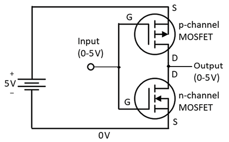
Figure 4.3: CMOS NOT gate circuit
When the Input signal is low (near 0 V), the lower n-channel MOSFET is switched off and the upper p-channel MOSFET is switched on. This connects the Output to the positive side of the voltage source, raising the Output signal to nearly 5 V. When Input is high, the upper MOSFET is switched off and the lower MOSFET is switched on, pulling the Output down to near 0 V. The Output signal is always the inverse of the Input signal, which represents the behavior of a NOT gate.
Today, virtually all high-density digital integrated circuits are based on CMOS technology. In addition to performing logic functions, the MOSFET is a key component of modern random-access memory (RAM) circuit architecture. The next section discusses the use of the MOSFET in memory circuits.
Constructing DRAM circuits with MOSFETs
A single bit in a standard dynamic random-access memory (DRAM) integrated circuit is composed of two circuit elements: a MOSFET and a capacitor. The following section presents a brief introduction to the electrical characteristics of capacitors.
The capacitor
A capacitor is a two-terminal passive circuit element capable of storing energy. Energy enters and leaves a capacitor as electrical current. The voltage across the capacitor terminals is proportional to the quantity of electrical energy contained in the capacitor.
To continue the hydraulic system analogy introduced in Chapter 2, Digital Logic, think of a capacitor as a balloon attached to the side of the pipe leading to a water tap. Water pressure in the pipe causes the balloon to inflate, filling it with some of the water from the pipe. Let’s assume this is a strong balloon, and that as it inflates, the balloon stretches, increasing the pressure within. The balloon fills until the pressure in the balloon equals the pressure in the pipe, and it then stops filling.
If you open the tap at the end of the pipe all the way, the release of water causes the pressure in the pipe to decrease. Some of the water in the balloon will flow back into the pipe until the balloon pressure again equals the pipe pressure.
Hydraulic devices called water hammer arrestors function in exactly this manner to solve the problem of pipes that make banging noises when water taps are turned on and off. A water hammer arrestor uses balloon-stretching-like behavior to smooth out the abrupt changes in water pressure that result from taps opening and closing.
The quantity of electrical energy contained in a capacitor is analogous to the amount of water in the balloon. The voltage across the capacitor is analogous to the pressure inside the balloon exerted by stretching.
An electrical capacitor can be constructed from two parallel metal plates separated by an insulating material, such as air. One terminal is connected to each of the plates. The ratio of the quantity of stored electrical energy to the voltage across the capacitor is called capacitance. Capacitance depends on the size of the parallel plates, the distance separating them, and the type of material used as the insulator between them. The capacitance of a capacitor is analogous to the size of the balloon in the hydraulic example. A capacitor with a larger capacitance corresponds to a larger balloon. A large balloon requires more water to fill to a given pressure than a small balloon.
The schematic symbol for a capacitor is shown in the following figure:

Figure 4.4: Capacitor schematic symbol
The two horizontal lines with space between them represent the metal plate capacitor architecture described in this section. The unit of capacitance is the farad, named after the English scientist Michael Faraday, who, among many other achievements, invented the electric motor.
The DRAM bit cell
A DRAM bit cell is a readable and writeable storage location for a single bit of data. A DRAM module in a modern computer or phone contains billions of bit cells. A single bit in a DRAM circuit consists of a MOSFET and a capacitor, arranged as follows:
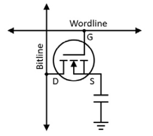
Figure 4.5: DRAM bit cell circuit
In this figure, the symbol with three horizontal lines at the bottom right is the ground symbol, which is the standard representation of the 0 V reference voltage we used in earlier diagrams such as Figure 4.3. The wordline and bitline are wires used to connect the individual bit cells into a grid.
This single-bit cell is replicated in a rectangular grid to form a complete DRAM memory bank. The following figure shows the configuration of a 16-bit DRAM bank consisting of 4 words of 4 bits each:
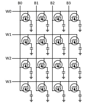
Figure 4.6: DRAM memory bank organization
Of course, real DRAM banks contain a much larger number of bits than the simple circuit shown here. Typical DRAM devices have a word size of 8 bits, rather than the 4 bits labeled B0-B3 in the figure. This means a DRAM chip can store or retrieve 8 bits in parallel.
The number of instances of bit cells along a wordline in an actual DRAM bank array is an integer multiple of the device word size. The large DRAM modules used in personal computers contain many words along each wordline. For example, a DRAM chip implemented with 8-bit words and 1,024 words per row contains 8,192 bits in a row, with all the MOSFET gate terminals along the row controlled by a single wordline signal. These devices contain additional multiplexer logic to select the specific word the processor is requesting from the many words along the row selected by the active wordline.
The vertical dimension of the DRAM bank consists of replicated copies of cell rows with one wordline controlling each row. The wordline connects all the bit cells horizontally, while the bitline signals connect the cells in all the rows vertically.
The state of each memory bit is stored in the cell’s capacitor. A low voltage on the capacitor represents a 0 bit, while a high voltage represents a 1 bit. In the context of DDR5 DRAM devices, low voltage is near 0 V and high is near 1.1 V.
The wordline for each row is held low most of the time. This keeps the MOSFET turned off, maintaining the capacitor state. When it is time to read a word (actually, an entire row) of DRAM, addressing circuitry selects the appropriate wordline and drives it high while keeping all the other wordlines in the bank low. This turns on the MOSFET in each bit cell along the active wordline, allowing the cell capacitors to drive their voltages onto the connected bitlines. Bitlines for cells at the 1 (high) voltage level will have higher voltages than cells at the 0 (low) voltage level. The bitline voltages are sensed by circuitry in the DRAM device and latched into the chip’s output register.
Writing to a DRAM word begins by setting the selected wordline high in the same manner as reading a word. Instead of sensing the voltage on the bitlines, the DRAM device drives each bitline with the voltage to be written to each cell, either 0 V or 1.1 V, depending on whether the data bit is a 0 or a 1. As with filling or emptying a balloon, it takes a bit of time for each capacitor to charge or discharge to the voltage presented on its bitline. After this delay has completed, the wordline is driven low to turn the MOSFETs off and lock the capacitors at their new charge levels.
DRAM circuit technology is complicated by the fact that capacitors leak. After charging a capacitor to a non-zero voltage, the charge bleeds off over time, reducing the voltage across the capacitor. Because of this, the contents of each cell must be refreshed periodically.
A refresh operation reads each cell value and writes it back to the cell. This recharges the capacitor to its “full” voltage level if it is a 1, or drives it to near 0 V if it is a 0. A typical refresh interval for modern DRAM devices is 64 milliseconds. DRAM refresh proceeds continuously, row by row, in the background during system operation and synchronizes with processor access to memory to avoid conflicts. There is a small performance penalty that occurs when processor access to memory is delayed by refresh activity.
While the need for periodic refreshing significantly complicates the design of systems using DRAM devices, the benefit of storing a bit with just one transistor and one capacitor is so immense that DRAM has supplanted all alternatives as the preferred technology for main memory in consumer, business, and scientific computer systems.
The next section will examine the architecture of the current generation of DRAM technology, DDR5.
DDR5 SDRAM
Intel produced the first commercial DRAM integrated circuit in 1970. The Intel 1103 held 1,024 bits and had a word size of 1 bit. The 1103 had to be refreshed every 2 milliseconds. By the early 1970s, MOS semiconductor DRAM overtook magnetic core memory as the preferred memory technology in computer systems. DRAM is volatile, meaning when power is removed, the charge in the bit cell capacitors dissipates and the data content is lost.
The term double data rate (DDR) refers to the transfer timing characteristics between a memory module and the processor memory controller. The original single data rate (SDR) DRAM performed one data transfer per memory clock cycle. DDR memory devices perform two transfers per clock cycle: one on the clock rising edge and one on the falling edge. The number following “DDR” identifies the generation of DDR technology. DDR5, therefore, is the fifth generation of the DDR standard. The term synchronous DRAM (SDRAM) indicates the DRAM circuitry is synchronized with the processor memory controller by a shared clock signal. The current generation of DRAM technology in widespread use is DDR4 SDRAM, while DDR5 SDRAM is beginning to roll out.
Modern personal computers and personal devices such as smartphones generally contain multiple gigabytes (GB) of RAM. One GB is 230 bytes, equivalent to 1,073,741,824 (just over one billion) bytes. As the name implies, random access memory allows the processor to read or write any memory location within the RAM address space in a single operation. As of 2021, a high-end memory module available for use in laptop computers contains 32 GB of DRAM distributed across 16 integrated circuits. Each DRAM chip in this module contains 2 giga-words, (where 1 giga-word is 230 words) with a word length of 8 bits.
In 2021, the leading memory module standard is DDR5 SDRAM, an evolutionary optimization of DRAM interface technologies built upon the DDR1, DDR2, DDR3, and DDR4 generations. A DDR5 memory module is packaged as a dual inline memory module (DIMM). A DIMM has electrical contacts on both sides of the circuit board edge (hence the term dual in the name), providing connectivity to the DIMM socket in the motherboard. A standard DDR5 DIMM has 288 pins. A smaller module format called the small outline DIMM (SODIMM) is available for systems such as laptops where space is at a premium. A DDR5 SODIMM has 262 pins. Because of the reduced number of pins, SODIMM modules lack features that some DIMMs support, such as the ability to detect and correct bit errors in data retrieved from the device. This capability is referred to as error correcting code (ECC).
DDR5 memory modules are nominally powered by 1.1 V. As a representative example, a particular DDR5 module can perform up to 4.8 billion data transfers per second, double the memory clock speed of 2,400 MHz. At 8 bytes per transfer, this DDR5 device can theoretically transfer 38.4 GB per second. DDR5 modules will be available in a variety of clock speeds, memory sizes, and price points.
Although real-world DRAM modules implement rectangular banks of single-bit cells as described in the previous section, the internal architecture of a DDR5 device is somewhat more complex. A DRAM integrated circuit generally contains multiple banks. The addressing logic selects the bank containing the desired memory location before performing a read or write operation. In DDR5 modules, banks are further arranged into bank groups, necessitating additional addressing logic to choose the correct group. A DDR5 device contains up to eight bank groups, each with up to four banks. The reason for partitioning the DDR5 module architecture into multiple bank groups is to maximize data transfer speed by enabling multiple simultaneous, overlapped memory access operations to proceed in parallel. This permits data transfer between processor and RAM to flow at peak speed while minimizing the need to wait for each DRAM access operation to complete.
In addition to specifying the correct address location within a DDR5 memory module, the system must provide a command via interface signals to indicate the action to be taken, specifically, whether to read from, write to, or refresh the selected row.
The DDR5 SDRAM standard, available for purchase from the Joint Electron Device Engineering Council (JEDEC) at https://www.jedec.org/standards-documents/docs/jesd79-5, provides the detailed definition of the DDR5 memory interface to host computer systems. This standard contains all the information needed to design memory modules compatible with any computer system supporting DDR5.
Historically, each numerical generation of the DDR SDRAM standards has been incompatible with previous generations. A motherboard built for DDR5 memory modules will only work with DDR5 modules. The slot for each DDR generation is constructed in such a way that it is not possible to insert an incorrect module. For example, a DDR4 DRAM module will not fit into a DDR5 slot.
As memory technologies evolve, the primary improvements in each new generation are increased data transfer rate and greater memory density. To assist in achieving these goals, power supply voltages have decreased in later generations, reducing system power consumption and enabling denser memory circuitry while avoiding excessive heating.
Most modern processors view system memory as a linear array of sequential addresses. In less sophisticated processor architectures, such as the 6502, the processor directly addresses RAM chips using memory addresses provided in instructions. Because of the complexity of the control signals and bank management logic in DDR5 SDRAM devices, modern computer systems provide a memory controller to translate each linear processor address into command and addressing signals selecting the appropriate DDR5 module (in a system with multiple memory modules), bank group, bank, and row/column location within the selected bank. The memory controller is a sequential logic device that manages the details of communication between the processor and DRAM memory modules. To achieve peak system performance, the memory controller must intelligently exploit the capability for overlapped operations provided by DDR5 memory modules.
Sophisticated modern processors generally integrate the memory controller function into the processor integrated circuit itself. It is also possible to design a system with a separate memory controller that sits between the processor and RAM.
A memory controller interface may contain multiple channels, where each channel is a separate communication path between the processor and one or more memory modules. The benefit of providing multiple channels in a memory architecture is that this configuration permits simultaneous memory accesses over the channels. However, a system containing multiple memory channels does not achieve an automatic increase in memory access speed. System software must actively manage the assignment of memory regions to each application or system process to balance memory usage across channels. If the operating system were to simply assign processes to physical memory regions sequentially, filling one memory module first then moving to the next, there would be no benefit from multi-channel memory because all processes would be forced to use the same memory channel.
Graphics DDR
Graphics DDR (GDDR) is a DDR memory technology optimized for use as video RAM in graphics cards. GDDR has a wider memory bus to support the high-throughput requirements of video displays. Standard DDR memory, on the other hand, is optimized to provide minimum latency access to data.
The generation numbers for GDDR and DDR are not aligned. As of 2021, GDDR6 modules have been available for a few years, while the DDR6 SDRAM standard remains in development.
Prefetching
One DRAM performance attribute that improves very little from one generation to the next is the speed of reading from or writing to an individual bit location. To achieve an increase in the average data transfer rate into and out of DRAM modules, the devices must employ other techniques to improve performance. One technique for achieving faster average data transfer speeds is prefetching.
The idea behind prefetching is to exploit the fact that whenever a particular memory location is being accessed by a processor, it is likely that addresses close to the first location will soon be accessed. Prefetching consists of reading a larger block of memory than the single address a processor instruction references and passing the entire block from the DRAM device to the processor. In the context of a DDR5 memory module, the block size is normally 64 bytes.
The DDR5 module can read 64 bytes quickly because it accesses all 512 bits of those 64 bytes simultaneously. To do this, the DDR5 module reads an integer multiple of 512 bitlines from the cells selected by a wordline. The bits of the selected row are read simultaneously, then pass through a multiplexer to extract the desired 512 bits from (perhaps) 8,192 bits in the entire row, which are then latched into an output register. The latched bits transfer from the DRAM module to the processor using DDR clocking.
With the effective use of multiple bank groups, multiple reads of memory and transfers of the resulting data can overlap in time and ensure that data moves between the memory module and the processor at the highest rate the interface can support.
Upon receiving the 64-byte block, the processor stores the data in internal cache memory and selects the specific data element (perhaps as small as 1 byte) from the block requested by the executing instruction. If a subsequent instruction accesses different data contained in the same block, the processor need only consult its local cache, resulting in much faster execution than the instruction that originally retrieved the data block from DRAM.
In addition to interacting with main memory, the processor must communicate with the outside world through input and output devices. The next section discusses the implementation of I/O interfaces in modern computer systems.
I/O subsystem
Chapter 3, Processor Elements, introduced two broad categories of I/O architecture: memory-mapped I/O and port-mapped I/O. The pros and cons of each of these approaches were significant in the early days of PCs when the number of physical address lines limited the total processor memory space to a 1 MB range. Modern processor architectures can address a far larger memory range, typically in the tens of gigabytes. A consequence of this address space expansion is the ready availability of address regions for use in I/O interfaces. Because of this, modern 32-bit and 64-bit general-purpose processors employ memory-mapped I/O for most of their interface requirements.
Sophisticated modern processors usually implement a memory controller within the processor chip, communicating directly with DDR memory modules. Most other types of I/O performed by these processors are offloaded to one or more external integrated circuits, typically referred to as a chipset. The term chipset is commonly used even when only one chip is needed to implement the I/O functions.
The chipset provides interfaces to a wide range of peripherals, such as disk drives, network interface, keyboard, mouse, and many others via USB. Most of these interfaces are implemented using one form or another of a serial bus. The following sections introduce the most common I/O technologies employed in modern computers.
Parallel and serial data buses
A parallel data bus communicates multiple data bits simultaneously across separate conductors between two or more communication endpoints. Early PCs used parallel buses for functions such as connecting a printer to the computer. Over time, several limitations of parallel buses became apparent:
- Depending on how many bits the bus supports, a parallel bus connection may require a lot of wires. This means cables are more expensive and there is a greater possibility of problems when cable wires break, or connectors fail to make solid electrical contact.
- As computer system developers made efforts to increase bus data rates (and thereby gain a competitive edge), another limitation of parallel buses became significant: even though the device transmitting a data word on the bus may output all the parallel bits simultaneously, the individual signals may not arrive at the destination at the same time.
This could be caused by differences in the effective path length of the conductors in the cable or across the circuit board. Because of this, there is an upper limit on the data transfer rate a parallel bus architecture can support.
Another limitation of parallel buses is they can only transfer data in one direction at a time (referred to as half-duplex) unless a duplicate set of connections is provided for simultaneously transferring data in the opposite direction. Parallel buses usually do not provide simultaneous bi-directional communication capability, referred to as full-duplex operation, for this reason.
A serial data bus transfers data between two communication endpoints a single bit at a time using a pair of conductors. Most high-speed communication paths between the processor and peripheral devices in modern computers use some form of serial bus. While, at first blush, switching from a parallel bus architecture to a serial bus seems to represent a substantial loss in throughput capability, serial buses exhibit several important advantages that make their use attractive in performance-critical applications.
High-speed serial buses in personal and business computer systems communicate over pairs of conductors using differential signaling. Differential signaling employs two conductors, carefully matched to be of the same length and to exhibit nearly identical electrical characteristics. When used in cables, these conductors are insulated wires twisted around each other to form twisted pairs.
The following figure represents a serial data bus using differential signaling:
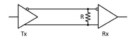
Figure 4.7: Serial bus circuit using differential signaling
The digital signal to be transmitted arrives at the transmitter (labeled Tx) via the input at the left side of the figure. The input is transformed into a pair of voltages on the two parallel lines crossing the center of the diagram. The small circle indicates the upper signal from the transmitter is inverted relative to the lower signal.
In a typical serial interface, a high signal level at the transmitter input will generate a voltage of 1.0 V on the top serial conductor and 1.4 V on the bottom conductor. A low signal input produces 1.4 V on the top conductor and 1.0 V on the bottom conductor.
The inputs to the receiver (which is labeled Rx) are high impedance, meaning the receiver draws negligible current from the circuit. The receiver measures the voltage across the resistor, which has a typical value of 100 Ω. When the Tx input is high, the upper resistor terminal is at -0.4 V relative to the lower terminal. When the Tx input is low, the upper resistor terminal is +0.4 V relative to the lower terminal.
The receiver produces its output signal by inverting one of the inputs (the top one in the figure, with the small circle) and adding the resulting voltage to the other input. In other words, the receiver only measures the difference between the voltages on the two conductors. The fundamental benefit of this approach derives from the fact that most forms of corrupting interference cause voltage variations in the conductors carrying the signal. By placing the two conductors very close together, most of the noise voltage introduced on one of the conductors will also appear on the other. The subtraction operation cancels out a large portion of the noise that would otherwise interfere with accurate signal detection by the receiver.
A serial data bus can perform several billion bit transfers per second, far more than an old PC’s parallel bus. It is also possible to run several serial buses alongside each other, effectively multiplying the data transfer bandwidth by the number of buses.
A crucial difference between multiple serial buses connecting two endpoints and a parallel bus making the same connection is that, for many interface standards, the serial buses operate somewhat independently. They do not synchronize at the level of each bit transfer in the same way all the bits in a parallel bus must. This makes it easier to design interconnections capable of supporting very high data rates with only the need to worry about precisely matching conductor length and electrical characteristics within each pair of serial conductors.
The connection between a modern processor and its motherboard chipset generally consists of several serial data buses called high-speed input output (HSIO) lanes. Each lane is a serial connection with one data path, like Figure 4.7, flowing in each direction, supporting full-duplex operation.
Individual HSIO lanes can be assigned to specific types of peripheral interfaces that are implemented as serial connections, such as PCI Express, SATA, M.2, USB, and Thunderbolt. The following sections introduce each of these interface standards.
PCI Express
The original Peripheral Component Interconnect (PCI) bus was a 32-bit parallel bus running at 33 MHz used in PC-compatible computers from about 1995 through 2005.
The PCI slots on computer motherboards accepted a wide variety of expansion cards performing functions such as networking, video display, and audio output. By the early 2000s, the limitations of the parallel bus architecture had become constraining, and development began on a serial bus replacement for PCI named PCI Express.
PCI Express, abbreviated as PCIe, is a bi-directional differential signaling serial bus used primarily to connect communication endpoints on computer motherboards. PCIe performance is expressed in billions of transfers (giga-transfers) per second, or GT/s. One “transfer” is a single bit propagated across the bus from transmitter to receiver. PCIe inserts additional redundant bits in each multi-bit communication to ensure data integrity. Different generations of PCIe have varying numbers of these overhead bits, influencing the effective data transfer rate. The following table shows the major generations of PCIe, the year each was introduced, the single-lane transfer rate in GT/s, and the effective data transfer rate in MB/s:
|
PCIe generation |
Year introduced |
Transfer rate |
Effective one-way data rate |
|
1.0a |
2003 |
2.5 GT/s |
250 MB/s |
|
2.0 |
2007 |
5 GT/s |
500 MB/s |
|
3.0 |
2010 |
8 GT/s |
985 MB/s |
|
4.0 |
2017 |
16 GT/s |
1,969 MB/s |
|
5.0 |
2019 |
32 GT/s |
3,938 MB/s |
|
6.0 (proposed) |
2021 |
64 GT/s |
7,877 MB/s |
Table 4.1: PCI Express generations
The effective data rate presented here is for one-way communication. PCIe supports full-speed data transfer in both directions simultaneously.
The PCIe standards support multi-lane connections indicated by the notations x1, x2, x4, x8, x16, and x32. Most modern motherboards implement, as a minimum, PCIe x1 and x16 slots. PCI x1 slots are compatible with a board edge connector length of 25 mm, while x16 slots expect a board edge connector length of 89 mm. A PCIe card will operate correctly in any slot in which it can physically fit. For example, a PCIe x1 card can be plugged into an x16 slot and will use just one of the 16 available lanes.
A primary application for PCIe x16 slots is to interface between the processor and a graphics card, with the goal of providing peak performance for graphics-intensive applications such as gaming. A PCIe 5.0 x16 interface is capable of unidirectional data transfer at 63 GB/s.
In modern computer architectures, the processor chip usually provides a direct PCIe 16-lane connection to a graphics board installed in a PCIe x16 slot. This means you don’t need to pass the graphics card PCIe signals through the chipset.
Other than the graphics display and the DDR SDRAM interface, most I/O in modern computer systems is managed by the chipset. The processor and chipset communicate through a collection of HSIO lanes. The chipset provides interfaces to peripheral devices such as disk drives, network interfaces, keyboard, and mouse. The interfaces to these devices commonly use the SATA, M.2, and USB serial interface standards, discussed next.
SATA
The Serial AT Attachment (SATA) is a bi-directional serial interface standard for connecting computer motherboards to storage devices. The “AT” in SATA refers to the IBM PC AT. Like a single PCIe lane, SATA contains two differential signaling pairs of conductors, where one pair carries data in each direction. Unlike PCIe, SATA is intended for operation over cables rather than over metal signal traces on motherboards. In addition to electrical and data format requirements, the SATA standard contains detailed specifications for compatible cables and connectors.
A SATA cable contains one bi-directional lane supporting communication between a processor and a storage device such as a magnetic disk drive, optical disk drive, or solid-state drive. The following table shows the major revisions of the SATA standard, the year each was introduced, and performance parameters:
|
SATA generation |
Year introduced |
Transfer rate |
Effective one-way data rate |
|
1.0 |
2003 |
1.5 GT/s |
150 MB/s |
|
2.0 |
2004 |
3 GT/s |
300 MB/s |
|
3.0 |
2009 |
6 GT/s |
600 MB/s |
Table 4.2: SATA generations
The data transfer rate in this table describes one-way communication, though, like PCIe, SATA supports full-duplex data transfer.
The SATA standard continues to undergo incremental improvements, but as of 2021 there has been no announcement of an upcoming SATA generation with a faster data transfer rate.
M.2
Modern solid-state drives (SSDs) employ flash memory to store data rather than the rotating magnetic platters in traditional hard drives. Because of the radically different technology of SSDs, the SATA interface that works well enough in most cases for rotating disks has proven to be a significant performance barrier for SSDs.
To access an arbitrary block of data (called a sector) on a magnetic disk drive, the drive head must physically move to the track containing the sector, then wait for the beginning of the sector to rotate to the head position before the drive can begin reading data. In contrast, an SSD can directly address any data sector in a manner very similar to the way a processor accesses a DRAM location.
The M.2 specification was developed to provide a small form factor and high-performance interface for flash memory storage in small, portable devices. The performance limitations of the SATA interface are removed, and it is possible to transfer data at rates several times faster than SATA can support.
In addition to mass storage devices, M.2 supports other interfaces including PCIe, USB, Bluetooth, and Wi-Fi. Modern motherboards include M.2 slots, which, in addition to the higher performance, consume much less space in the computer case than traditional disk drive bays.
USB
The USB interface provides a simple (from the user’s viewpoint) interface for connecting a wide variety of peripheral devices to a computer system. In addition to communication protocols, the USB standard revisions define requirements for cables, connectors, and for supplying power to connected devices via the USB cable.
USB cables have easily identifiable connector types and USB-enabled devices support hot-plugging (plugging devices together while powered on). USB devices are self-configuring, and, in most cases, users need not concern themselves with installing drivers when attaching a new device to a computer with a USB cable.
Early USB data cables (through generation 2.0) contained a single differential signaling pair that could pass data in only one direction at a time. Later versions of the USB standard (USB 3.2 Gen 1 onward) support simultaneous bi-directional data transfer. In addition, USB generations 3.2 and USB4 provide up to two lanes, doubling the data transfer rate.
The following table shows the major revisions of the USB standard, the date each was introduced, the maximum number of lanes supported, and peak data transfer performance:
|
USB generation |
Year introduced |
Number of lanes |
Transfer rate |
Effective one-way data rate |
|
1.1 |
1998 |
1 |
0.012 GT/s |
1.5 MB/s |
|
2.0 |
2000 |
1 |
0.48 GT/s |
60 MB/s |
|
3.2 Gen 1 |
2008 |
1 |
5 GT/s |
500 MB/s |
|
3.2 Gen 2 |
2013 |
1 |
10 GT/s |
1,200 MB/s |
|
3.2 Gen 2x2 |
2017 |
2 |
20 GT/s |
2,400 MB/s |
|
USB4 |
2019 |
2 |
40 GT/s |
4,800 MB/s |
Table 4.3: USB generations
In USB generations through 2.0, communication takes place entirely under the control of the host. The host initiates each communication interaction by sending packets addressed to a particular device and performs data transfers to or from the device. Beginning with USB 3.2 Gen 1, devices can initiate communication with the host, effectively providing an interrupt capability for connected peripherals.
Thunderbolt
Thunderbolt is a collection of high-speed serial interface standards introduced in 2011. The original Thunderbolt interface combined PCIe and DisplayPort signal transmission using two serial Thunderbolt lanes.
Thunderbolt 4 is the latest generation of the Thunderbolt standard, adding USB4 compatibility while supporting connectivity to PCIe devices and to multiple high-resolution displays from a single computer port. Thunderbolt 4 uses the same connector as USB 3.2 and later generations (the USB-C connector) and supports the 40 Gbit/s USB4 data rate. USB devices operate properly when connected to a computer’s Thunderbolt 4 port. Thunderbolt 4 peripheral devices are not compatible with non-Thunderbolt 4 USB-C ports, however.
The next section provides an overview of the most popular graphics display interface standards.
Graphics displays
In the domains of gaming, video editing, graphic design, and animation, video processing performance is critical. Generating and displaying high-resolution graphics requires an enormous number of mathematical calculations.
While general-purpose processors can perform the necessary computations, such processors lack the performance users of these applications have come to expect.
High-performance graphics cards, called graphics processing units (GPUs), are essentially miniature supercomputers, heavily optimized to perform graphical computational tasks such as 3D scene rendering. Because the computations involved in scene rendering are highly repetitive, substantial performance gains can be achieved with the use of hardware parallelization. Graphics processors contain a large number of relatively simple computational units, each performing a small portion of the overall task.
A GPU may contain thousands of individual processing units that each function like an ALU. While the original driving force that led to the development of high-performance GPUs was 3-D scene generation, later generations of this technology have found broad use in fields such as big data analytics and machine learning. Any numerically intensive computational task that can be broken into a collection of parallel operations is suitable for acceleration with a GPU architecture.
Of course, not all users require extreme video performance. To accommodate users with modest graphics needs and more limited budgets, modern processors often integrate a moderately capable GPU into the processor chip. In many applications, this approach provides more than adequate graphical performance. This configuration is referred to as integrated graphics, meaning the GPU function is integrated into the processor die and shares system memory with the processor. Computer systems with integrated graphics are lower in cost while providing adequate graphics performance for basic computing tasks such as email, web browsing, and watching videos.
Many desktop computer systems, as well as some laptops, provide integrated graphics while offering the option of installing a high-performance graphics card. This allows users to tailor the computer system to their price and performance needs.
Several different video standards are in current use for connecting displays to computers. Because the output generated by a computer graphics interface must be compatible with the connected display, it is common for computers to provide more than one type of video connector. Computer monitors and high-definition televisions usually provide a selection of video connection types as well.
Chapter 6, Specialized Computing Domains, will cover the processing architecture of GPUs in more detail. The following sections describe video interface standards used in computer applications past and present.
VGA
The Video Graphics Array (VGA) video standard for personal computers was introduced by IBM in 1987. VGA is an analog interface that remains in widespread use today, though most modern computers do not provide a VGA connector. It is not uncommon to find older computers with VGA outputs using a converter cable to present a display on a monitor supporting DVI or HDMI video input.
Modern versions of the VGA standard support display resolutions up to 1,920 pixels wide by 1,200 pixels high, refreshed at 60 Hz. Because the VGA video signal is analog, some loss of signal quality occurs during transmission to the display. This effect is most noticeable at high screen resolutions.
DVI
The Digital Visual Interface (DVI) video standard was developed to improve the visual quality of computer displays by transferring the video signal digitally from the computer to the monitor. To maintain backward compatibility with older computers and monitors, DVI cables can carry VGA analog signals as well.
Like the high-speed serial interfaces discussed earlier in this chapter, DVI uses differential serial signaling to transfer video data. A DVI connector contains four serial lanes. Individual lanes carry red, green, and blue color information, and the fourth lane carries the common clock signal.
Three DVI variants are defined, depending on the combination of digital and analog video signal types supported:
- DVI-A supports only the analog video signal. This option is intended to provide backward compatibility with VGA computers and monitors. The DVI-A connector has a different pin layout than traditional VGA connectors, so an adapter cable is required to connect to legacy VGA devices.
- DVI-D is a digital-only interface supporting single-link and dual-link options. The dual-link option provides additional serial data lanes to increase the video bandwidth for higher-resolution displays. Dual-link does not mean the cable supports dual monitors.
- DVI-I is an integrated interface supporting both the analog interface of DVI-A and the digital modes of DVI-D. A DVI-I digital interface may be single- or dual-link.
DVI interfaces are used primarily in computer display applications. The effective data rate of a single-link DVI-D connection is 3.96 gigabits per second (Gbit/s). Dual-link DVI-D transfers video data at twice the single-link rate, 7.92 Gbit/s.
HDMI
High-Definition Media Interface (HDMI) is supported by most modern computers and monitors, and by virtually all modern televisions and related video entertainment devices such as DVD players. HDMI supports digital video only (there is no analog capability) and uses the same differential serial bus as DVI-D. In addition to video data, HDMI cables also transport multi-channel digital audio.
The HDMI standard has undergone several revisions since its introduction in 2002. Each successive revision has maintained backward compatibility while adding new capabilities. Later versions of the standard have increased video bandwidth, increased the range of supported screen resolutions, added high-definition audio capabilities, added support for Ethernet communication over the HDMI cable, and added features to support gaming. Although each HDMI version is backward compatible, newer features are only available in configurations where the signal source device, the display device, and the connecting cable are all compatible with the newer standard.
HDMI version 2.1 was released in 2017. This standard supports an effective data rate of 42.6 Gbit/s over four differential serial lanes.
DisplayPort
DisplayPort, introduced in 2006, is a digital interface standard supporting digital video, audio, and USB connections. While HDMI is targeted at consumer electronics such as televisions and home theater systems, DisplayPort is oriented toward computer applications. DisplayPort transfers data in packets with clocking information embedded in each packet, eliminating the need for a separate clock channel.
A single computer DisplayPort output can drive multiple monitors connected in a daisy chain, where one cable connects the computer to the first monitor, a second cable connects the first and second monitors, and so on. The monitors must provide support for this capability. The maximum number of displays that can be combined in this manner is limited only by the capabilities of the graphics card, the maximum cable data throughput, and the resolution and refresh rate of the displays.
DisplayPort 2.0 was released in 2019, with an effective data rate of up to 77.4 Gbit/s over four differential serial lanes.
Network interface
A computer network is a collection of digital devices interacting over a shared communication medium. A local area network (LAN) consists of a limited number of computers that might reside in a single physical location such as a home or office building. The connected computers, phones, and other digital devices in your home represent a LAN. Device connections within a LAN environment may use a wired interface, usually Ethernet, or a wireless interface, typically Wi-Fi.
Geographically separated computers and LANs communicate using a wide area network (WAN). WAN services are often provided by a telecommunication company such as a cable television provider or telephone company. Your home LAN most likely connects to the Internet via WAN services provided by your telephone or cable company.
Home and business network interface devices (called routers) provided by WAN service providers usually offer Ethernet and Wi-Fi options for connecting local devices to the WAN. The following sections introduce the technologies of Ethernet and Wi-Fi.
Ethernet
Ethernet is a set of networking standards for connecting computers using cables in a LAN environment. The original version of Ethernet was developed by Robert Metcalfe at Xerox Palo Alto Research Center in 1974. Ethernet was released commercially in 1980 as a 10 Mbit/s communication technology for groups of computers connected with coaxial cabling. The name of the technology was derived from the historical term luminiferous aether, a hypothesized medium filling all of space and enabling the propagation of electromagnetic waves. The Ethernet cable serves as a conceptually similar communication medium.
The Institute of Electrical and Electronic Engineers (IEEE) began developing standards for LAN technologies, including Ethernet, in 1980. The IEEE 802.3 Ethernet standard was published in 1985. Since then, the standard has undergone several revisions supporting increased data rates and different network topologies. The most obvious difference in modern computer networks from the original Ethernet standard is the use of point-to-point twisted pair cables in place of the original shared coaxial cable.
Modern computers commonly use Gigabit Ethernet interfaces to communicate over unshielded twisted-pair (UTP) cabling. Gigabit Ethernet is formally defined in the IEEE 802.3ab standard and supports 1.0 Gbit/s with an effective data transfer rate up to 99% of the raw bit rate, though the amount of overhead varies considerably depending on the communication protocol in use.
Ethernet communication is composed of variable-size data units called frames containing up to 1,518 bytes. The header of each frame contains addressing information identifying the source and destination Ethernet interfaces. Because modern twisted-pair connections are point-to-point, the most common structure for connecting a group of computers is to run a cable from each computer to a switch. A switch is a device that receives frames transmitted by the connected computers and, based on the destination address contained in each frame, immediately forwards it to the correct recipient. Ethernet cables are limited to a maximum recommended length of 100 meters, constraining the physical size of an Ethernet LAN to an area such as a single office building or home.
Modern motherboards usually contain a built-in Ethernet interface, which eliminates the need to consume a PCIe slot with an Ethernet card. An Ethernet interface, whether built into the motherboard or installed in a PCIe expansion slot, consumes one HSIO lane connecting from the processor through the chipset to the Ethernet interface.
Wi-Fi
The IEEE released the first version of the 802.11 wireless communication standard in 1997 supporting a raw data rate of 2 Mbit/s in the 2.4 GHz radio frequency band. The 802.11b standard, released in 1999 with an 11 Mbit/s raw data rate, proved to be commercially popular. The technology was named Wi-Fi in 1999 as a reference to the term “hi-fi,” referring to high-fidelity sound reproduction.
The 802.11g standard, released in 2003, has a raw bit rate of 54 Mbit/s. 802.11n, released in 2009, supports multiple-input-multiple-output (MIMO) antennas and optional operation in the 5 GHz band. The 802.11ac standard, published in 2013, supports a bit rate in the 5 GHz band of over 500 Mbit/s using MIMO antenna configurations. The 802.11ax standard, approved in 2021, provides a 39% throughput increase relative to 802.11ac for a single client and offers enhanced support for use in dense radio signal environments. 802.11ax is marketed as Wi-Fi 6 for operation in the 2.4 and 5 GHz bands and as Wi-Fi 6E for operation in the 6 GHz band.
Wi-Fi devices can suffer from interference produced by household appliances such as cordless phones, microwave ovens, and other Wi-Fi networks in the area. Wi-Fi signal propagation is affected by factors such as walls and other obstacles between transmitter and receiver, multipath (the destructive interference between a direct-path signal and a reflected copy of the signal), and is limited by the maximum power a Wi-Fi transmitter is authorized to emit. The use of multiple antennas in 802.11n, 802.11ac, and 802.11ax configurations significantly mitigates multipath-related performance issues.
Modern WAN routers supplied by telecommunication service providers usually contain a combination of Ethernet and Wi-Fi communication interfaces. A primary benefit of Wi-Fi in comparison to Ethernet for these applications is the reduction in the amount of cabling required.
One drawback of Wi-Fi is the potential for security issues because the radio frequency signal can propagate far outside the building containing the communicating systems. The Wi-Fi standards provide substantial support for secure communication using protocols such as Wi-Fi Protected Access 2 (WPA2), but system administrators and users must ensure the appropriate security features are enabled and that secret information such as the network password is sufficiently complex and is stored securely.
Support for Wi-Fi is ubiquitous in portable digital devices such as laptops, smartphones, and tablets, and is directly built into many motherboards.
The next section presents the computer interfaces with the lowest bandwidth requirements: the keyboard and mouse.
Keyboard and mouse
Compared to the high-speed interfaces discussed earlier in this chapter, the bandwidth requirements for a keyboard and mouse are quite modest. These devices are the sole input methods used by the human operator in most computer configurations, and thus are only required to operate at the speed of human actions. Even the fastest typist can only press one or two dozen keys per second.
Keyboard
A mechanical computer keyboard consists of a collection of keys, each of which activates an electrical momentary switch. A standard full-size keyboard typically contains 104 keys including the arrow keys, control keys (Home, Scroll Lock, and so on), and the numeric keypad. Modern keyboards commonly use a USB cable for connection to the computer or connect wirelessly.
Because the bandwidth requirements for human interaction are so low, some computer motherboards provide a slower USB 2.0 port for keyboard connection while offering higher-performance USB 3.2 or faster interfaces for high-speed peripherals. This results in a small cost reduction for the motherboard components.
Because the keyboard reports the press and release of each key separately, the computer can process combinations of keys pressed simultaneously. For example, holding the Shift key down while pressing the A key produces a capital A.
Some computers and digital devices such as tablets and phones provide a touchscreen interface. When text input is required on these devices, the system displays a keyboard pattern on the screen and the user touches letter locations to produce keypresses.
Mechanical keyboards tend to provide more accurate input and are favored by users entering significant quantities of text. Because the surface of a touchscreen is completely flat, there is no feedback to the user’s fingers indicating alignment with the keys. This results in more frequent input errors when using touchscreen keyboards. Of course, when using a touchscreen keyboard there is no need to provide a mechanical keyboard, which represents a substantial benefit for portable devices. In addition, touchscreen keyboard input does not suffer from mechanical failures that can affect the components of mechanical keyboards. For users wearing gloves, text input is more difficult on both touchscreens and keyboards.
Mouse
A computer mouse is a hand-held device that moves a pointer horizontally and vertically across a computer screen. The user initiates actions based on the pointer location by pressing buttons on the mouse. Modern mice often provide a small wheel capable of rolling in either direction, used to perform tasks such as scrolling through a document.
As with the keyboard, the mouse commonly connects to the computer via USB over a wired or wireless connection. The mouse has low bandwidth requirements and can be supported on a USB 2.0 port.
The operation of a mouse requires a flat horizontal surface, typically a table top, upon which the user moves the mouse. Modern mice most commonly use optical emitters and sensors to detect motion across the surface. Many mice have difficulty operating on highly reflective surfaces such as glass tabletops.
A trackball is similar in concept to a mouse, except that rather than moving a mouse across a surface, a ball is retained at a fixed location but is allowed to rotate in any direction using hand motion. By rolling the ball forward, backward, left, and right, the user can move the pointer on the computer display.
A trackball does not require the amount of surface space a mouse needs, and the trackball can be fixed at a stationary location. The ability to firmly attach a trackball to a structure makes the trackball the preferred pointing device for computer stations installed in ground vehicles, ships, and aircraft.
As with the keyboard, the computer detects the press and release of each mouse button as separate events. Users can exploit this capability to perform operations such as dragging an icon across the screen by following these steps:
- Place the pointer over the icon
- Press and hold the left mouse button
- Move the pointer (with the icon now attached) to the new location
- Release the mouse button
Together, the keyboard and mouse provide all the input capability most computer users need to perform their interactive tasks.
The next section brings together the subsystem descriptions in this chapter to examine the specifications of a modern computer motherboard.
Modern computer system specifications
With the information in this chapter, you should be able to interpret most of the technical features of a modern computer motherboard, processor, and chipset. This section provides an example of the specifications for a current (2021) motherboard with some explanation of the individual features.
The designers of a computer motherboard must make several decisions such as the number of PCIe expansion ports, number of DIMM slots, number of USB ports, and the number of SATA ports to be provided in a particular motherboard model. These decisions are guided by the target customer demographic, whether it be gamers, business users, or cost-conscious home users.
The example motherboard presented here is the ASUS Prime X570-Pro, a higher-performance board intended for gaming applications that supports gaming-related features such as overclocking. Overclocking refers to increasing the clock frequencies for the processor and other system components with the goal of improving performance.
Overclocking increases heat generation and may lead to unstable performance if a component is driven at an excessive frequency.
Table 4.4: Example motherboard specifications
This example is intended to provide some perspective on the specifications of higher-end consumer-grade computer capabilities as of 2021.
If you are looking to purchase a computer, you can use the information in this chapter to make yourself a more informed consumer.
Summary
This chapter began with an introduction to the computer memory subsystem, the MOSFET, and the capacitor. We examined the circuitry that implements the DRAM bit cell. We reviewed the architecture of DDR5 memory modules and the operation of multichannel memory controllers. Other types of I/O devices were introduced, with a focus on high-speed differential serial connections and their ubiquitous use in technologies such as PCIe, SATA, USB, and video interfaces.
Popular video standards were presented, including VGA, DVI, HDMI, and DisplayPort. We looked at the Ethernet and Wi-Fi networking technologies as well. We continued with a discussion of standard computer peripheral interfaces including the keyboard and mouse. The chapter concluded with a description of an example modern motherboard, highlighting some of its interesting features.
With the information presented in this chapter, you should have a solid understanding of modern computer components from the level of technical specifications down to the technologies used in implementing the circuitry.
In the next chapter, we will explore the high-level services computer systems must implement, such as disk I/O, network communications, and interactions with users. We’ll examine the software layers that implement these features, starting at the level of the processor instruction set and registers. Several key aspects of operating systems will be covered including booting, multithreading, and multiprocessing.
Exercises
- Create a circuit implementation of a NAND gate using two CMOS transistor pairs. Unlike NPN transistor gate circuits, no resistors are required for this circuit.
- A 16-gigabit DRAM integrated circuit has two bank group selection inputs, two bank selection inputs, and 17 row address inputs. How many bits are in each row of a bank in this device?
Join our community Discord space
Join the book’s Discord workspace for a monthly Ask me Anything session with the author: https://discord.gg/7h8aNRhRuY